Significance
Semiconductor point defects have shown great promise in their application to quantum information and sensing in the solid state. However, it is an ongoing challenge to efficiently access the light emitted by these spin-active defects and, furthermore, to enhance the emission at wavelengths that can be used to create indistinguishable photons. Such emission enhancement can be achieved by placing the defects within optical microcavities. Here, using 1D photonic crystal cavities, we report the significant enhancement of point-defect emission in silicon carbide, which hosts a suite of intriguing spin-active defects. In addition to measuring large enhancements, we also demonstrate how the cavity coupling can potentially allow access to a variety of information about the defects and their environment.
Keywords: cavity coupling, Purcell enhancement, silicon carbide, point defect, photonic crystal cavity
Abstract
Point defects in silicon carbide are rapidly becoming a platform of great interest for single-photon generation, quantum sensing, and quantum information science. Photonic crystal cavities (PCCs) can serve as an efficient light–matter interface both to augment the defect emission and to aid in studying the defects’ properties. In this work, we fabricate 1D nanobeam PCCs in 4H-silicon carbide with embedded silicon vacancy centers. These cavities are used to achieve Purcell enhancement of two closely spaced defect zero-phonon lines (ZPL). Enhancements of >80-fold are measured using multiple techniques. Additionally, the nature of the cavity coupling to the different ZPLs is examined.
Spin-active point defects in a variety of silicon carbide (SiC) polytypes have recently elicited a great deal of interest as the basis for solid-state single-photon sources, nanoscale quantum sensing, and quantum information science (1–10). Such color centers in SiC offer access to emission at a variety of wavelengths, ranging from visible (600–800 nm) (7) to near-IR (850–1,300 nm) (1, 2, 6). Furthermore, in many polytypes, such as 4H- and 6H-SiC, the diatomic lattice and the crystal structure lead to a wider variety of defect properties than, for example, in diamond. For instance, the silicon vacancy (SiV) center can occupy either hexagonal or cubic lattice sites, exhibiting differences in the zero-phonon line (ZPL) emission wavelength and the zero-field spin splitting, depending on which site hosts the vacancy (11–14). Similar variation is seen in the neutral divacancy (1). Thus, SiC defects yield a wide variety of properties that can be selected as desired and these defects can provide high sensitivity to subtle variations in their local environments.
Readout of such local information can be greatly augmented by coupling these point defects to high-quality optical cavities which can enhance their optical emission properties, enabling large increases in the emission rate into their ZPLs (15–18). A number of groups have fabricated photonic crystal cavities in SiC, achieving passively measured (i.e., without emitters in the cavity) quality factors, Q, at telecom frequencies of 103–104 in 3C-SiC (19–21) and 6H-SiC and of ∼7 × 10⁴ in amorphous SiC (22). Other work has shown cavity-enhanced measurements of a 3C-SiC color center (23, 24). However, there have not yet been demonstrations of significant coupling to and enhancement of the ZPL emission from SiC point defects.
In this work, we report such enhancement in high-Q, 1D nanobeam photonic crystal cavities (PCCs) with embedded SiV centers in 4H-SiC. We selectively couple to two closely spaced ZPL transitions, and achieve enhancement of greater than ∼80-fold, comparing the increase in the ZPL intensity on- and off-resonance with the cavity mode. The degree of enhancement is also confirmed by measurement of the spontaneous emission fraction into the cavity-enhanced ZPL and measurement of fluorescence lifetime decrease on-resonance. In addition, we demonstrate the responsiveness of the cavity to temperature-induced changes in the ZPL populations as well as to the polarization properties of the two transitions. Therefore, the cavity-coupling work demonstrated here represents important progress in the field of SiC defect photonics, both paving the way toward the improved functionality of SiC defects for quantum sensing and information as well as establishing the role of the cavities themselves in providing valuable insights into the study of these defects.
Results
As in our previous work, we use a PCC design that provides a high theoretical quality factor, Q, with a small mode volume, V (25, 26). Such parameters are desirable given that the degree of emission enhancement provided by the cavity can be quantified by the Purcell factor (27),
| [1] |
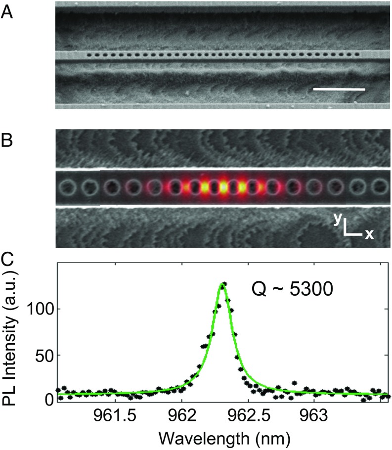
The factor ξ takes into account the spectral and spatial overlap of the cavity field with the emitter being enhanced, as well as the alignment of the cavity field and the emitter’s optical dipole. With perfect overlap and alignment, ξ is 1. Thus, for a given ξ, maximizing emission enhancement depends upon fabricating cavities with high Q and low V. To provide high Q/V, the PCC design we have chosen consists of a linear array of holes (Fig. 1A), where the eight innermost holes on either side of the center are linearly tapered to define a cavity region. The holes are tapered in both their center-to-center spacing and their parallel-to-beam diameter (x axis in Fig. 1B), creating elliptical holes in this inner region. For both parameters, the minimum tapered value is 84% of the values in the outer holes. Finite-difference time-domain (FDTD) simulations (Lumerical Solutions) confirm that these cavities have high theoretical Q of 4 × 10⁶ and small mode volume of 0.45 (λ/n) (3), where λ is the resonant wavelength of the cavity mode and n the refractive index. The simulated electric-field profile of the primary transverse electric (TE) mode is shown Fig. 1B, showing that the fields are well localized to the inner, tapered cavity region.
Fig. 1.
Nanobeam PCC and mode. (A) SEM micrograph of 1D nanobeam PCC with embedded SiV centers. (Scale bar, 2 μm.) (B) Detailed view of inner cavity region of the PCC with overlaid electric field profile from FDTD simulations. (C) Measured cavity mode coupled to SiV luminescence showing high-quality factor Q of 5,300. Lorentzian fit to measured data is shown in green.
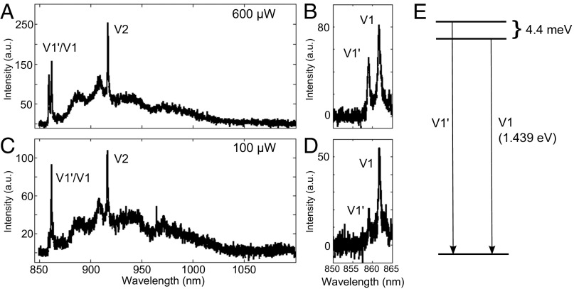
The fabrication technique we used, described in Materials and Methods, resulted in chips with ∼3,000 cavities, designed with cavity resonances that span the full range of the SiV emission. The point defects were introduced after the fabrication of the cavities: The wafers with PCCs were ion implanted (Cutting Edge Ions Inc; Materials and Methods) without postannealing to create ensembles of SiV centers. Based on comparison with other work (9, 28) quantifying the creation of these centers in 4H-SiC, we expect a few tens (∼10–30) of defect centers within the cavity mode volume. Photoluminescence (PL) spectra of the implanted samples taken at 4 K in a helium-cooled continuous-flow cryostat (Janis) show the positions of the ZPLs of both the V1 and V2 types of the SiV center. These two centers correspond to the two inequivalent Si lattice sites in 4H-SiC, with V1 belonging to the cubic (k) site and V2 to the hexagonal (h) site (12). The defects at both sites have total spin S = 3/2 and show optically detected magnetic resonance signals (3, 4, 12). As seen in Fig. 2, the V1 ZPL is observed at 861.4 nm and the V2 ZPL at 916.5 nm, corresponding to values previously reported in literature. Moreover, the V1 center is known to have a high-temperature companion ZPL, typically denoted V1′, stemming from a transition to an excited state of slightly higher energy than the excited state corresponding to the V1 transition (13). Because of the 4.4-meV energy splitting between the V1′ and V1 excited states (schematic shown in Fig. 2E), the intensities of the corresponding ZPLs are temperature dependent (13). This is clearly observed in the spectra shown in Fig. 2: When the excitation laser is at a power of 100 μW, emission into the V1′ line is suppressed (Fig. 2 C and D). However, at a higher excitation laser power of 600 μW, the V1′ transition intensity is nearly comparable to that of the V1 peak due to laser-induced heating (Fig. 2 A and B). At the higher laser power, the branching ratio into each ZPL is ∼1–1.3%, whereas at lower laser power the branching ratio into the V1 line is ∼1.6% with only ∼0.5% into the V1′ line.
Fig. 2.
SiV spectrum and ZPL intensity. (A) Full spectrum of SiV luminescence measured with 600-μW excitation power at 4K. The V1′, V1, and V2 ZPLs are all visible and indicated. (B) High-resolution spectrum showing V1′ and V1 ZPLs measured with 600-μW excitation power at 4 K. (C and D) Same as A and B with 100-μW excitation power. Here, the V1′, whose intensity is temperature-dependent, has much lower intensity due to much reduced laser-induced heating. (E) Schematic showing energy level structure corresponding to V1 and V1′ ZPL emission.
After ion implantation, we characterized the fabricated PCCs using confocal PL microscopy. A pulsed Ti:sapphire laser tuned to a wavelength of 760 nm was used to optically excite the SiV centers in the cavities, and the emitted light was passed to a spectrometer for analysis. Measured PCC spectra showed cavity modes decorating the defects’ broad PL signal (consisting primarily of phonon sideband emission). Even without postimplantation annealing of the material, the cavities displayed high values of Q, typically between ∼2,000 and 5,000 (Fig. 1C), as calculated by fitting the cavity spectrum to a Lorentzian profile. This disparity between measured and theoretical Q is commonly observed in fabricated PCC devices (16–18, 20, 23). As discussed in previous work (25), the measured Q is often limited by fabrication imperfections, particularly those linked to reactive ion etching, like roughness, angled sidewalls, and other ion-induced damage. Other limiting factors may include absorption by the SiVs introduced to the devices and by other defects also created by the ion implantation. Using Q of 2,000 and the simulated V of ∼0.45 (λ/n) (3) in Eq. 1, we calculate a maximum Purcell enhancement of ∼340, assuming ξ of 1. Even without perfect defect placement within the cavity, significant ZPL enhancement can be achieved, as long as the overlap of the defect spatial location and cavity field maximum is sufficient to yield ξ of ∼0.1 or greater.
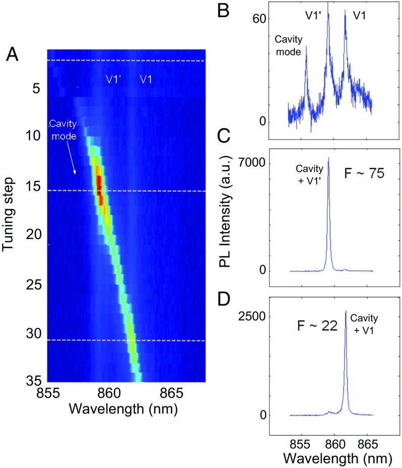
To demonstrate such enhancement, it is easiest to choose devices with modes that are slightly blueshifted from the desired ZPL wavelength and then slowly redshift the cavity mode through resonance, using nitrogen gas condensation (18). This technique is commonly used and can typically reversibly redshift cavity modes by at least 20 nm without degrading their Qs (17, 18, 22, 29). Modes can also be appropriately blueshifted of the ZPL by using previously reported techniques for tuning 4H-SiC cavities (25). Therefore, we selected cavities with well-coupled modes that were blueshifted relative to the 859.1-nm V1′ line and took measurements as these modes are tuned through both V1′ and V1 ZPLs. By focusing on the interaction with these two ZPLs, we use the cavity as an exquisitely sensitive probe of these transitions which have the same ground state and two different excited states. The results of this tuning with one such cavity using an excitation power of 600 μW are shown in Fig. 3. An intensity map as a function of tuning step in the vicinity of the V1 and V1′ ZPLs is shown in Fig. 3A. The excitation power and collection time were kept constant for each spectrum acquired so that the intensities could be directly compared. As labeled, the two fixed lines correspond to the V1 and V1′ ZPLs, through which the cavity mode sweeps as it is redshifted by the condensed gas. The intensity of each ZPL reaches a maximum when it coincides with the cavity mode wavelength.
Fig. 3.
Cavity mode tuning and ZPL enhancement at 600-μW excitation. (A) Intensity map showing the interaction of the cavity mode with the V1′ and V1 ZPLs as a function of nitrogen gas injection step. As the gas is injected, the cavity mode redshifts (as indicated), while the V1′ and V1 ZPLs remain fixed. For visibility, the square root of the intensity is plotted. The three dotted white lines correspond to cross-sections shown in B–D. (B) Spectrum taken when the cavity mode is far off-resonance, showing the cavity mode and the two ZPLs. (C and D) Spectra taken when the cavity is resonant with the V1′ and V1 ZPLs, respectively. The marked increase in intensity on-resonance can be clearly seen. As indicated, the V1′ line is enhanced ∼75-fold, and the V1 line is enhanced ∼22-fold on-resonance.
Additionally, Fig. 3 B–D provides details of the emission spectra at specific tuning steps to better underscore the increased emission into the ZPLs when they are resonant with the cavity mode. In Fig. 3B, we see the cavity mode far off-resonance from both ZPLs. At cryogenic temperatures, the defects emit very little light at the cavity wavelength, and therefore emission into the ZPLs is of low intensity. Fitting the spectrum reveals a cavity Q of ∼2,200. The corresponding FWHM of the cavity, 0.4 nm, is well matched to the ZPL linewidths (on the order of ∼0.5 nm), which aids in efficient coupling. In Fig. 3 C and D, the cavity mode is fully on-resonance with the V1′ and V1 ZPLs, respectively. The large corresponding increases in intensity are readily apparent and we moreover see that the on-resonance intensity of the V1′ is significantly higher than that of the V1. A typical means of quantifying the degree of Purcell enhancement, F, achieved by a cavity is to compare the on- and off-resonant ZPL intensity (17, 18). Indeed, with the cavity off-resonance, the total defect emission rate is given by (17)
where 1/τZPL is the emission rate into the zero-phonon line and 1/τPSB is the emission rate into the phonon sideband. This off-resonance emission rate within the cavity is still significant, but it may be reduced compared with the defect emission rate in bulk (as demonstrated later) due to the photonic bandgap effect (16). On-resonance, the cavity enhances the emission rate into the ZPL such that the total defect emission rate is given by
Therefore, as previously argued (17), the on- and off-resonant ZPL intensity can be compared with estimate of the Purcell enhancement of the defects by the relation
From this equation, we obtain an enhancement of 75 for the V1′ ZPL and 22 for the V1 ZPL in the cavity described in Fig. 3.
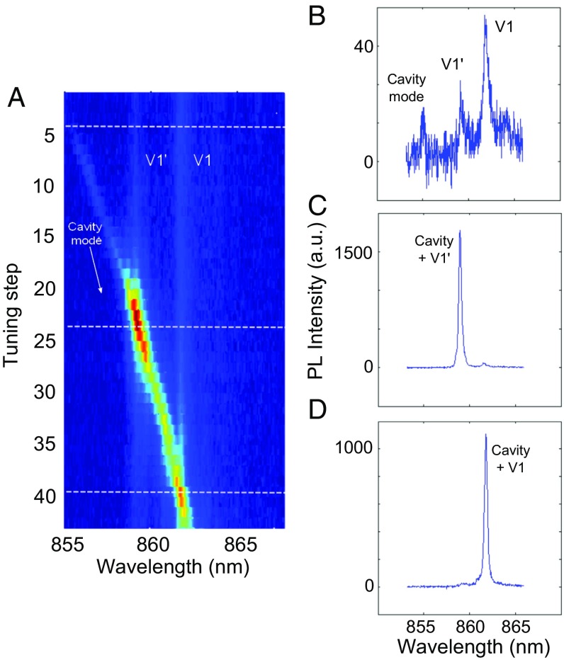
We then carried out the same cavity tuning but using a lower excitation power of 100 μW. These data are shown in Fig. 4, with Fig. 4 B–D showing the detailed spectra of the cavity mode far off-resonance and then on-resonance with the V1 and V1′ ZPLs. Using on- and off-resonance intensity measurements, we derive the same degree of enhancement as observed for the higher-power (600-μW) excitation: an enhancement of 75 for the V1′ ZPL and 22 for the V1 ZPL. However, although the cavity enhancement for both transitions is thus shown to be independent of excitation power used, the ratio of the on-resonance intensities for the V1′ vs. V1 ZPLs is much larger in the 600-μW (Fig. 3 C and D) case than in the 100-μW case (Fig. 4 C and D). This arises from the fact that the relative intensity ratio of the V1′/V1 ZPLs at 600 μW (∼1.3×), compared with at 100-μW excitation (∼3×), is the same whether on- or off-resonance. Thus, the cavity is quite specific in its enhancement of these two closely spaced and related transitions. Furthermore, by controlling both the excitation power and the ZPL to which the cavity is coupled, maximum contrast of emission into one ZPL or the other as desired can be achieved.
Fig. 4.
Cavity mode tuning and ZPL enhancement at 100-μW excitation. (A) Intensity map showing the interaction of the cavity mode with the V1′ and V1 ZPLs as a function of gas injection step. As in Fig. 3, the redshift of the cavity mode is indicated, and the three dotted white lines correspond to cross-sections shown in B–D. (B) Spectrum taken when the cavity mode is far off-resonance showing the cavity mode and the two ZPLs. (C and D) Spectra taken when the cavity is resonant with the V1′ and V1 ZPLs. Compared with Fig. 3, the relative intensities of the ZPLs on-resonance are much closer, because the V1′ line, whereas exhibiting a higher degree of enhancement, has much lower intensity than the V1 line at this excitation power. As in Fig. 3, the ZPL intensities are enhanced by factors of ∼75 and ∼22.
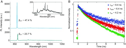
To confirm that we are achieving the spontaneous emission enhancement that is characteristic of the Purcell effect, we present further measurements on a second cavity, which showed the largest measured Purcell enhancement. We begin by considering the spontaneous emission factor, β, which can be calculated as the fraction of light emitted into the ZPL with the cavity mode on-resonance, (28). We can relate β to the Purcell factor by the equation (30)
where Γ is the branching ratio into the ZPL when the cavity is off-resonance. This can be rearranged to give
Fig. 5A shows the full PL spectra of this cavity. The upper and lower spectra show the cavity on-resonance with the V1′ and V1 ZPLs, respectively. Fig. 5A (Inset) shows the off-resonance spectrum. In this cavity, for the V1′ (V1) transitions, the values of β are 47.4% (23.7%), and the values of Γ are 1% (1.2%). These correspond to F ∼ 89 and ∼25 for the V1′ and V1 ZPLs, respectively, which match the values derived by comparing the total intensity of the ZPLs on and off-resonance, ∼90 and ∼26. Furthermore, these measurements demonstrate that the ZPL is being selectively enhanced without a corresponding increase in the sideband emission, as desired. Therefore, using these cavities, we are able to direct nearly half of the SiV emission into the V1′ ZPL, as opposed to the natural branching ratio of ∼1%. Achieving such an increase is extremely important for quantum information applications using these point defects (e.g., entanglement) that can only make use of ZPL emission (15–17).
Fig. 5.
Increase in ZPL spontaneous emission rates and reduction in fluorescence lifetime. (A) Full spectrum of cavity showing highest Purcell enhancement when on-resonance with V1′ ZPL (Upper) and V1 ZPL (Lower), labeled by the fraction of light emitted into the ZPLs on-resonance. (Inset) Spectrum taken when the cavity is blueshifted from both ZPLs. Nearly 50% of the SiV emission is directed into the V1′ ZPL on-resonance. (B) Fluorescence lifetime measurements when the cavity mode is blueshifted from the ZPLs (blue) and on-resonance with the V1′ ZPL (green). A lifetime measurement of the SiV in bulk (red) is also shown. As expected, the emitter lifetime is increased when the cavity mode is off-resonance and decreased when it is on-resonance.
We further corroborate the spontaneous emission enhancement by measuring the excited-state lifetime of the SiV defect on-resonance with the cavity. The Purcell enhancement can be calculated from lifetime measurements using the following relation (16, 29, 30):
Here, τon refers to the lifetime when the mode is on-resonance with the ZPL, τoff the lifetime when the mode is off-resonance, and τ0 the natural lifetime in the bulk material. When on-resonance, the fluorescence lifetime decreases from τ0 due to the increased photonic density of states. When the cavity analyzed in Fig. 5A was tuned into resonance with the V1′ ZPL, the ZPL emission was selected using a narrow bandpass filter (860-nm center wavelength, 10-nm FWHM) and passed to an avalanche photodiode for single-photon counting. Fig. 5B shows the resultant fluorescence decay signal (green curve), which is fit to yield an on-resonance lifetime of 4.2 ns. We also measure an off-resonance lifetime of 9.4 ns (blue curve) and a bulk lifetime of 6.4 ns (red curve). The bulk lifetime matches previous measurements of the silicon vacancy fluorescence lifetime (6). Moreover, as mentioned previously, the off-resonance lifetime is longer than the bulk lifetime due to a reduced density of states when the cavity mode is off-resonance with the ZPL. Using these values yields an estimated Purcell enhancement of 84, which substantiates the value estimated from measurements of ZPL intensity enhancement and increased spontaneous emission fraction into the ZPL.
Discussion and Conclusion
Lastly, we further explore the different enhancement factors for the V1′ ZPL compared with the V1 ZPL. The ∼3.5-fold greater enhancement of the V1′ ZPL in both cavities presented in this work is also recapitulated in measurements of all other cavities tuned through resonance. Because we are probing ZPLs that are very close spectrally, the Q and V of a given cavity change negligibly as it is tuned through resonance with both ZPLs. Moreover, because the ZPLs result from transitions of the same SiV centers (those sitting at the k lattice sites within the cavity volume), the emitter-field spatial overlap of the ensemble of defects being enhanced in a given cavity does not vary for the two ZPLs. Therefore, the most likely explanation for the difference in enhancement between the V1′ and V1 ZPLs is a difference in alignment between the cavity field vector and the emitter optical dipole. Our SiC crystal is grown along the c axis, and therefore the plane of the PCCs (and correspondingly the cavity mode polarization) is perpendicular to the c axis. Previous work has suggested that the V1′ transition is strongly polarized perpendicular to the c axis and the V1 transition is weakly polarized parallel to the c axis (13). Such polarization would explain the difference in enhancement between the two ZPLs well. Indeed, if the optical dipole for the V1′ transition is assumed to be nearly perpendicular to the c axis (and thus closely aligned to the cavity mode), the values of enhancement measured here would imply that the V1 optical dipole is polarized ∼60° from the V1′ dipole, giving an angle of ∼30° with the c axis.
In summary, we have demonstrated 1D nanobeam PCCs in 4H-SiC with high-quality factor modes (Q up to 5,300) coupled to silicon vacancy defect centers generated by ion implantation. Using high-Q cavities with resonances slightly blueshifted from two closely related silicon vacancy ZPLs, we used nitrogen gas condensation to controllably tune the cavity mode into resonance with these ZPLs. We observed Purcell enhancement of more than 80-fold and confirm these measurements by comparing on- and off-resonant intensities, increased spontaneous emission fraction into the ZPLs, and decreased defect fluorescence lifetime on-resonance. We were able to direct up to nearly half the light emitted by the SiV into the V1′ ZPL, a substantial improvement over the natural branching fraction. Additionally, the responsiveness of the cavity to changes in ZPL population and to differences in polarization shows that the cavity can serve as effective and highly sensitive probe to both amplify and study the optical properties of the defects. For example, it has been noted elsewhere that the optical signatures of the V1, V1′, and V2 defects are sensitive to strain in the material (13). These cavities could therefore provide precise and dynamic assessments of the local strain environments of defects at different characteristic sites in the SiC lattice. Thus, with the demonstrated ability to achieve a high degree of cavity–defect interaction in silicon vacancy centers in 4H-SiC, this work represents an important step in the development of point defects in SiC as a significant platform for solid-state quantum devices.
Materials and Methods
Sample Fabrication.
Electron-beam lithography (Elionix) is used to define the cavity pattern, which is transferred to an aluminum hard mask by reactive ion etching (RIE) (Unaxis Shuttleline). A second RIE step (STS ICP-RIE) transfers the pattern to the SiC wafer, which consists of a 250-nm p-type (Al, 5 × 1017 cm−3) epilayer homoepitaxially grown on an n-type substrate (N, 1019 cm−3). After pattern transfer, the n-type substrate is removed with a dopant-selective photoelectrochemical etch to provide optical isolation for the cavity (25, 31). This procedure allows us to create cavities out of high-quality epitaxially grown material.
Defect Implantation.
Silicon vacancy centers were created by implantation of 12C ions at a dose of 1012 ions per square centimeter and an energy of 70 keV. In the vertical dimension, the cavity field profile reaches its maximum value in the middle of the cavity, which is 125 nm below the surface for our 250-nm device layer. Therefore, the 70-keV ion energy was selected to create defects with a maximum probability at this depth, as calculated by stopping range of ions in matter simulations.
Acknowledgments
The authors acknowledge funding from the Air Force Office of Scientific Research, under the Quantum Memories in Photon-Atomic Solid State Systems (QUMPASS) program (Award FA9550-12-1-0004). This work was supported by the Science and Technology Center for Integrated Quantum Materials, National Science Foundation (NSF) Grant DMR-1231319. This work was performed in part at the Center for Nanoscale Systems (CNS), a member of the National Nanotechnology Infrastructure Network, which is supported by the National Science Foundation under NSF Award. ECS-0335765. CNS is part of Harvard University.
Footnotes
The authors declare no conflict of interest.
References
- 1.Koehl WF, Buckley BB, Heremans FJ, Calusine G, Awschalom DD. Room temperature coherent control of defect spin qubits in silicon carbide. Nature. 2011;479:84–87. doi: 10.1038/nature10562. [DOI] [PubMed] [Google Scholar]
- 2.Falk AL, et al. Polytype control of spin qubits in silicon carbide. Nat Commun. 2013;4:1819. doi: 10.1038/ncomms2854. [DOI] [PMC free article] [PubMed] [Google Scholar]
- 3.Baranov PG, et al. Silicon vacancy in SiC as a promising quantum system for single-defect and single-photon spectroscopy. Phys Rev B. 2011;83:125203. [Google Scholar]
- 4.Riedel D, et al. Resonant addressing and manipulation of silicon vacancy qubits in silicon carbide. Phys Rev Lett. 2012;109:226402. doi: 10.1103/PhysRevLett.109.226402. [DOI] [PubMed] [Google Scholar]
- 5.Widmann M, et al. Coherent control of single spins in silicon carbide at room temperature. Nat Mater. 2015;14:164–168. doi: 10.1038/nmat4145. [DOI] [PubMed] [Google Scholar]
- 6.Hain TC, et al. Excitation and recombination dynamics of vacancy-related spin centers in silicon carbide. J Appl Phys. 2014;115:133508. [Google Scholar]
- 7.Castelletto S, et al. A silicon carbide room-temperature single-photon source. Nat Mater. 2014;13:151–156. doi: 10.1038/nmat3806. [DOI] [PubMed] [Google Scholar]
- 8.Zargaleh SA, et al. Evidence for near-infrared photoluminescence of nitrogen vacancy centers in 4H-SiC. Phys Rev B. 2016;94:60102. [Google Scholar]
- 9.Fuchs F, et al. Engineering near-infrared single-photon emitters with optically active spins in ultrapure silicon carbide. Nat Commun. 2015;6:7578. doi: 10.1038/ncomms8578. [DOI] [PubMed] [Google Scholar]
- 10.Simin D, et al. High-precision angle-resolved magnetometry with uniaxial quantum centers in silicon carbide. Phys Rev Appl. 2015;4:14009. [Google Scholar]
- 11.Wimbauer T, Meyer BK, Hofstaetter A, Scharmann A, Overhof H. Negatively charged Si vacancy in 4H SiC: A comparison between theory and experiment. Phys Rev B. 1997;56:7384–7388. [Google Scholar]
- 12.Sörman E, et al. Silicon vacancy related defect in 4H and 6H SiC. Phys Rev B. 2000;61:2613–2620. [Google Scholar]
- 13.Wagner M, et al. Electronic structure of the neutral silicon vacancy in 4H and 6H SiC. Phys Rev B. 2000;62:16555–16560. [Google Scholar]
- 14.Janzén E, et al. The silicon vacancy in SiC. Physica B. 2009;404:4354–4358. [Google Scholar]
- 15.Aharonovich I, Neu E. Diamond nanophotonics. Adv Opt Mater. 2014;2:911–928. [Google Scholar]
- 16.Faraon A, Santori C, Huang Z, Acosta VM, Beausoleil RG. Coupling of nitrogen-vacancy centers to photonic crystal cavities in monocrystalline diamond. Phys Rev Lett. 2012;109:033604. doi: 10.1103/PhysRevLett.109.033604. [DOI] [PubMed] [Google Scholar]
- 17.Hausmann BJM, et al. Coupling of NV centers to photonic crystal nanobeams in diamond. Nano Lett. 2013;13:5791–5796. doi: 10.1021/nl402174g. [DOI] [PubMed] [Google Scholar]
- 18.Lee JC, et al. Deterministic coupling of delta-doped nitrogen vacancy centers to a nanobeam photonic crystal cavity. Appl Phys Lett. 2014;105:261101. [Google Scholar]
- 19.Lee JY, Lu X, Feng PX-L, Lin Q. 2014. 3C-SiC nanobeam optomechanical crystals. CLEO: 2014, OSA Technical Digest (Optical Society of America, Washington, DC), paper SF1M.2.
- 20.Radulaski M, et al. Photonic crystal cavities in cubic (3C) polytype silicon carbide films. Opt Express. 2013;21:32623–32629. doi: 10.1364/OE.21.032623. [DOI] [PubMed] [Google Scholar]
- 21.Yamada S, et al. Second-harmonic generation in a silicon-carbide-based photonic crystal nanocavity. Opt Lett. 2014;39:1768–1771. doi: 10.1364/OL.39.001768. [DOI] [PubMed] [Google Scholar]
- 22.Lee JY, Lu X, Lin Q. High-Q silicon carbide photonic-crystal cavities. Appl Phys Lett. 2015;106:41106. doi: 10.1063/5.0010078. [DOI] [PMC free article] [PubMed] [Google Scholar]
- 23.Calusine G, Politi A, Awschalom DD. Silicon carbide photonic crystal cavities with integrated color centers. Appl Phys Lett. 2014;105:11123. [Google Scholar]
- 24.Calusine G, Politi A, Awschalom DD. Cavity-enhanced measurements of defect spins in silicon carbide. Phys Rev Appl. 2016;6:14019. [Google Scholar]
- 25.Bracher DO, Hu EL. Fabrication of high-Q nanobeam photonic crystals in epitaxially grown 4H-SiC. Nano Lett. 2015;15:6202–6207. doi: 10.1021/acs.nanolett.5b02542. [DOI] [PubMed] [Google Scholar]
- 26.Zhang Y, McCutcheon MW, Burgess IB, Loncar M. Ultra-high-Q TE/TM dual-polarized photonic crystal nanocavities. Opt Lett. 2009;34:2694–2696. doi: 10.1364/OL.34.002694. [DOI] [PubMed] [Google Scholar]
- 27.Purcell E. Spontaneous emission probabilities at radio frequencies. Phys Rev. 1946;69:681. [Google Scholar]
- 28.Wang J, et al. 2016. High-efficiency generation of nanoscale single silicon vacancy defect array in silicon carbide. arXiv:161003978.
- 29.Li L, et al. Coherent spin control of a nanocavity-enhanced qubit in diamond. Nat Commun. 2015;6:6173. doi: 10.1038/ncomms7173. [DOI] [PubMed] [Google Scholar]
- 30.Zhong T, Kindem JM, Miyazono E, Faraon A. Nanophotonic coherent light-matter interfaces based on rare-earth-doped crystals. Nat Commun. 2015;6:8206. doi: 10.1038/ncomms9206. [DOI] [PMC free article] [PubMed] [Google Scholar]
- 31.Magyar AP, Bracher D, Lee JC, Aharonovich I, Hu EL. High quality SiC microdisk resonators fabricated from monolithic epilayer wafers. Appl Phys Lett. 2014;104:51109. [Google Scholar]


