Abstract
Purpose
The purpose of this study is to develop an in-bore RF power amplifier (RFPA) module with high power efficiency and density for use in parallel transmit (pTX) arrays at 3 T.
Methods
The modules use a combination of current mode class D (CMCD), class S, and class E amplifiers based on enhancement-mode silicon-on-gallium nitride FETs (eGaN FETs). Together the amplifiers implement envelope elimination and restoration (EER) to achieve amplitude modulation with high efficiency over a wide operating range. The static nonlinearity and power efficiency of the module were measured using pulsed RF measurements over a 37 dB dynamic range. Thermal performance was also measured with and without forced convection cooling.
Results
The modules produces peak RF power up to 130 W with an overall efficiency of 85%. When producing 100 W RF pulses at a duty cycle of 10%, maximum junction temperatures did not exceed 80 °C, even without the use of heatsinks or forced convection.
Conclusion
The small size and low cost of the modules promise lower cost implementation of pTX systems compared to linear RFPAs located remotely. Further work must be done on control of the RF output in the presence of nonlinearities and coupling.
Keywords: Parallel transmit, RF chain, RF power amplifier, array decoupling
Introduction
Local amplifiers for pTX
Radiofrequency (RF) excitation using an array of parallel transmit coils has been proposed as a solution to challenges associated with very high field (VHF) and ultra high field (UHF) MRI, including B1 inhomogeneity (1–3) and SAR management (3–7). This is predicated on the ability of the transmit array to accurately produce independent RF pulses on each channel. This control is complicated by several matters, including subject loading, RF chain nonlinearity, and coupling between channels. Numerous techniques have been explored to address array coupling and linearity. These include cancellation by predistortion (8–10), coil current feedback (11–13), and RF power amplifiers (RFPAs) with high power mismatches on their outputs (14,15).
A second major challenge of pTX is the numerous RF power cables required to carry RF power from the RFPAs (typically located outside the scanner room) to the array elements. Long RF power cables cause power loss in the array, and also contribute significant size and cost to the system (16). Additionally, the use of long cables is problematic for the previously mentioned decoupling methods. Losses in the cables decrease the effectiveness of amplifier decoupling using power mismatch. Feedback-based approaches require current or field sensors on each element, and these sensors must have their own cables leading back to the array controller(s), adding additional cost and complexity.
To address these challenges, it has been proposed to locate the RF power amplifiers on or near the array elements rather than remotely (14,16–18). Multiple long RF power cables could be replaced with a single shared DC power feed, which would be much more power efficient. The RF inputs to the amplifiers would be delivered over small, low-power RF cables. Additionally, locating the RFPAs closer to the transmit coils would simplify coil current measurement and feedback. Overall, the amount of cabling entering the scanner bore could be greatly reduced.
However, locating the power amplifiers inside or near the magnet bore also presents new engineering challenges. In particular, heating near the patient and cryostat must be limited. Also, the amplifiers must be operable within a strong magnetic field, and must not introduce significant B0 distortion in the imaging volume.
To address the restrictions of near-coil amplifiers, it was proposed by Heilman et al (19) to use the Current Mode Class D (CMCD) amplifier topology, which boasts higher power density and efficiency than the more common class AB RFPAs, for a high-efficiency on-coil amplifier. Later work by Guidino et al (12) showed the use of the CMCD topology in combination with modulation via the Kahn technique (20) and output current magnitude feedback (OCMF) in a compact in-bore transmit amplifier module. Previously we demonstrated the use of Enhancement Mode Gallium Nitride on Silicon FETs (eGaN FETs) as a replacement for LDMOS FETs in a prototype 63.6 MHz CMCD amplifier module (21). Here we will demonstrate a new design for in-bore operation at 123.25 MHz (3 T). We will show that eGaN FETs offer extremely high power efficiency and density for switchmode RFPAs at 123 MHz.
CMCD topology
Evaluating the utility of amplifiers for MRI transmit requires an overview of the unique needs of the MRI experiment. Firstly, MRI transmit requires the RFPA to operate with a high peak to average power ratio (PAPR). Most RF pulse shapes are similar to a windowed sinc pulse, with a duration normally on the order of milliseconds (22). An example sinc pulse with two zero crossings (N=2) and a Hanning window will have a PAPR of 7 dB. The overall amplitudes of the pulses may also vary by over an order of magnitude within a sequence. These factors together result in high overall PAPR for the MRI experiment. Many RFPAs used in MRI pTX systems are typically linear classes such as A, B or AB. Class A and B amplifiers have theoretical maximum efficiencies of 50% and 79% respectively, with class AB lying in between, depending on the conduction angle. The maximum efficiency occurs at the maximum output power. Below the maximum output power, efficiency scales by a factor of Pout/Pmax for class A and for class B. Therefore, class AB amplifiers will have lower overall power efficiency as PAPR is increased (23), which typically makes class AB amplifiers unsuitable for in-bore MRI RFPAs without substantial cooling systems. Previously it has been shown that envelope tracking can be applied to the class AB amplifier to improve power efficiency across a wider power range, but the amplifier is still limited to its theoretical efficiency constraints (24).
Secondly, the RF power must be delivered into the bore of the MRI scanner, which is a restricted space with a powerful static magnetic field. Heat dissipation must be limited to protect the subject and the magnet itself. Given that VHF and UHF MRI systems may require total RF power of over 30 kW, even modest inefficiencies can result in a large amount of heat dissipated in the bore.
Both of these issues can be addressed by using a high-efficiency switchmode amplifier topology. In particular, the CMCD topology (25) has been demonstrated in past work for MRI transmit applications (12,19). In the CMCD topology, two transistors are operated as passive switches rather than as dependent current or voltage sources. When properly tuned, the drain voltage approximates a half-sinewave with peak amplitude of π · VB, where VB is the drain bias voltage. The circuit is ideally tuned to achieve zero voltage switching (ZVS), which eliminates losses due to hard switching of COSS, unlike in the voltage mode class D (VMCD) topology where COSS causes significant losses. The CMCD is theoretically capable of operating at 100% efficiency over its full output power range. In practice, the losses in a properly tuned CMCD amplifier consist only of conduction in the transistors and surrounding passive components, and dissipation required for gate drive.
The primary disadvantage of the CMCD topology is that amplitude modulation can only be efficiently implemented with the Kahn technique (20), whereby the bias voltage VB to the amplifier is varied. This may result in poor linearity when implemented with real devices. However, nonlinearities can, in principle, be corrected with control methods such as predistortion and output feedback. Power inefficiency, on the other hand, cannot be recovered with such control techniques. Therefore we propose that for in-bore amplifiers, power efficiency should take precedence over linearity.
eGaN FETs
Linear and switchmode power amplifiers put different requirements on the power transistors. Linear amplifier classes such as classes A, B, and AB operate their FET(s) mainly in the saturation region, and benefit from high transconductance, high breakdown voltage, low distortion, and high transition frequency. Switchmode RFPAs, on the other hand, operate their FET(s) mainly in the cutoff and Ohmic regions, and benefit more from low RDS(on), low junction capacitances, high breakdown voltage, and fast switching speeds. With the exception of breakdown voltage, these sets of parameters are not necessarily well correlated, and thus devices optimized for linear amplifiers, including the majority of LDMOS devices, are not necessarily suitable for use in the CMCD topology.
In previous work (21), we introduced the use of eGaN FETs for use in the CMCD topology in an attempt to improve upon LDMOS for an on-coil RFPA. eGaN FETs are capable of improved performance relative to Si due to the inherently superior material characteristics of GaN, which has a higher electron mobility, saturation velocity, and breakdown voltage than Si devices can achieve (26). Additionally, eGaN FETs were originally optimized for switchmode power conversion rather than linear amplification. Table 1 shows a comparison of several performance parameters between three eGaN FETs (EPC2007, EPC2012C, and EPC2038 from EPC Corporation) and two LDMOS RF FETs, (MRF136 from MA-COM Technology Solutions and the MRF6V2010NR1 from Freescale Semiconductor).
Table 1.
Properties of select LDMOS and eGaN FETs. RDS(ON) of the LDMOS devices was measured at VGS=10 V and ID=0.2 A. Device area refers to the smallest possible rectangle. All other values taken from the device datasheets.
| EPC2007 | EPC2012C | EPC2038 | MRF136 | MRF6V2010NR1 | |
|---|---|---|---|---|---|
| VDSS (V) | 100 | 200 | 100 | 65 | 110 |
| RDS(ON) (Ω) | 0.03 | 0.1 | 2.8 | 1.4 | 4.0 |
| COSS (pF) | 118 | 64 | 1.7 | 27 | 7.3 |
| RDS · COSS (Ω · F) | 3.5 E-12 | 6.4 E-12 | 4.8 E-12 | 38 E-12 | 29 E-12 |
| Area (mm2) | 1.9 | 1.6 | 0.81 | 400 | 121 |
The EPC2007 and EPC2012C have far lower on-state resistance than the LDMOS devices, suggesting they are capable of handling much higher current. Their output capacitance is, however, significantly higher, which limits their operating frequency. In contrast, the EPC2038 has similar on-state resistance to the LDMOS FETs with much lower COSS, implying it could provide similar currents but at much higher frequencies.
The benefits of the underlying eGaN FET technology is evident in the product of RDS(on) and COSS for each device. This figure of merit is at least 6 times lower than either LDMOS device at similarly rated VDSS. The eGaN devices were also far smaller than the LDMOS devices, which is convenient for on-coil amplifiers where space is limited. The die packaging of eGaN FETs is also more suitable to the CMCD topology due to its minimal equivalent series inductance (ESL). However, the small package size also limits heat transport from the devices, which may limit overall power capability. The cost of eGaN FETs is also less than LDMOS FETs with equivalent output power ratings.
Methods
Architecture
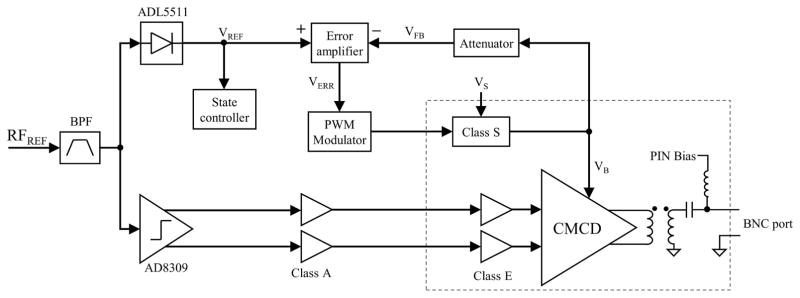
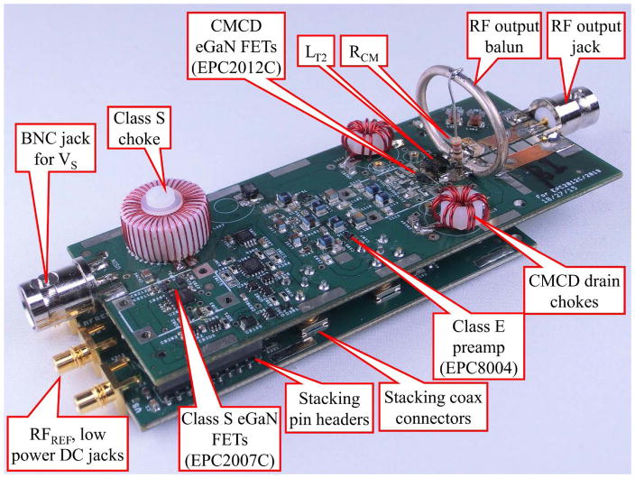
Figure 1 shows a photograph of the RFPA module. The module was designed to operate as a standalone module requiring only a single RF control input as well as external fixed DC sources. The module should produce an amplitude modulated RF output which is proportional to the low power RF input. Thus from a black box perspective the module performs much like a linear RF power amplifier. To achieve this, the envelope elimination and restoration (EER) technique is used (20). Figure 2 shows a block diagram of the module’s architecture. The module is constructed using two separate printed circuit boards in a stacked configuration. The bottom PCB contains all the low power control and signal conditioning systems, while the top PCB contains the higher power circuitry, including the class S amplifier, CMCD stage, and class E gate drivers.
Figure 1.
Photograph of the assembled RFPA module.
Figure 2.
Block diagram of the module architecture. Area inside the dashed box represents contents of the power board.
The module is fed DC power over three coaxial cables. Two cables carry +6 V and −11 V which are converted to +5 V and −10 V on the module by low dropout linear regulators to bias the low power circuitry. A third cable carries VS, the bias for the class S amplifier (typically VS=48 V DC). A fourth coaxial cable is used to carry the RF reference to the module from the scanner’s RF synthesizer. In principle, only one DC power supply is necessary, and the RF reference could also use the same cable, thus allowing the module to operate with only one coaxial cable. Separate cables were used in this work in order to easily distinguish power drawn by different parts of the module.
Envelope elimination
Unlike the module described in (12), in which control signals were generated from a nonstandard, external data timing generator in polar form (consisting of a RF carrier and a baseband envelope signal) and transmitted via fiber optic cable, our module is intended to be used with the modulated RF output of the standard MRI synthesizer, referred to here as the RF reference (RFREF). The RFREF from the scanner is taken as the reference in a negative output feedback loop which regulates the bias voltage VB applied to the CMCD stage.
RFREF first passes through a third order 123 MHz Chebyshev bandpass filter. The filtered reference is split and fed to an envelope detector (ADL5511, Analog Devices) and a carrier recovery amplifier (AD8309, Analog Devices). The envelope detector’s output VREF provides the reference level for the VB control loop. The carrier recovery amplifier provides a fixed amplitude differential carrier with the same phase and frequency as RFREF. Each differential carrier output is further amplified to +18 dBm (SGA-4586Z, RFMD Inc.). These are then fed to class E amplifiers (EPC8004, Efficient Power Corporation), which drive the gates of the eGaN FETs in the CMCD output stage.
Various parts of the module can be enabled or disabled depending on whether the RFPA is in its idle state or active state. When VREF is above 40 mV (equivalent to −20 dBm of power on RFREF), the module is put in its active state. In the active state, all amplifier stages are enabled and the PIN diode driver sources up to 100 mA. In the idle state, the RF preamplifier chain is deactivated, the class S amplifier is disabled, and the PIN diode driver output is at −10 V. Total power comsumption from the +5/−10 V supply rails was 2.05 W in the active state and 0.23 W in the idle state.
Envelope restoration
The magnitude of the module’s output is controlled through the Kahn technique, whereby the magnitude of the RF output is modulated by controlling the bias voltage VB of the CMCD stage. As in previous work, the modulation of VB is done using a class S amplifier consisting of a half bridge inverter and a LC output filter. The filter inductor was 4.26 μH and the output filter capacitor was 2.5 μF. The filter choke was wound on a 3D printed toroidal former with 40 turns of AWG 28 magnet wire. VB was connected to the CMCD stage using 150 nH chokes which used M5 nylon nuts as toroidal formers with 12 turns of AWG 22 magnet wire. Toroidal chokes were used to carry large DC currents in order to mitigate their distortion on the static field and to minimize the resulting Lorentz forces. To accommodate the higher power and voltage required by the 3 T design, the class S amplifier uses EPC2007C eGaN FETs.
Previous work made us of output current magnitude feedback (OCMF). In OCMF, the measured magnitude of the coil current is compared to the magnitude of the RFREF, and and a negative feedback loop varies the bias voltage VB to the RFPA in order to force them to be proportional. This was done in order to reduce AM-AM nonlinearity in the amplifier and reduce the effect of coupling and load variation on coil current. However subsequent work (27) demonstrated that OCMF is limited since it cannot correct the phase of the RF output. However, it was also shown that amplifier decoupling with passive impedance transformers can be more effective overall at suppressing deviation in output current. While the control board was able to accommodate the necessary circuitry to implement OCMF, we chose not to make use of it for this work based upon these findings.
The VB controller in the 3 T module consists of a type III error amplifier whose output feeds a 1.25 MHz PWM modulator, which drives the class S amplifier. The negative input of the error amplifier is fed by an attenuated VB, while its positive input is fed by VREF. This forces VB to be proportional to the magnitude of RFREF. The K-factor approach (28) was used to determine the error amplifier response in order to achieve a loop crossover frequency of 200 kHz and a 60° phase margin.
NTC thermistors were also added nearby the eGaN FETs in the Class S and CMCD amplifiers so that their temperatures could be estimated. The resistance of each thermistor is converted to a voltage by auxiliary circuitry on the control board, and these voltages were sampled during each RF pulse.
CMCD PA stage
In addition to the doubling of the operating frequency, we targeted a twofold increase in maximum output power (125 W) for the 3 T module. We also wanted the 3 T module’s output to be compatible with unbalanced 50 Ω loads, in contrast to the 1.5 T module which was meant to connect directly to a series resonant coil. Therefore we made use of the EPC2012C eGaN FET (RDSON=100 mΩ, VDSS=200 V) as the power FETs in the CMCD stage. A 1:1 transmission line transformer was used to convert the balanced output of the CMCD into an unbalanced output. The magnetizing inductance of the balun (approximately 60 nH) also functioned as part of the tank inductance LT for the CMCD. Another shunt inductor LT2 was also used in parallel with the balun’s primary to adjust the overall LT value for optimal efficiency at maximum output power. A PIN diode driver circuit is also coupled to the RF output with a bias tee, so that active PIN diode detuning can be used on the RF coil.
At such high operating frequencies, layout parasitics make implementing square wave gate drive waveforms impractical with discrete components. Instead, we use sinewaves to drive the gates of the eGaN FETs in the class E preamplifiers and the CMCD stage. Figure 3 shows a schematic of one half of the differential RF chain on the power board.
Figure 3.
Schematic of one half of the differential RF chain on the power board.
One challenge specific to eGaN FETs is that there is little margin between the optimal gate drive voltage (5 V) and the absolute maximum rating of VGS (−4 V to 6 V). Overdrive of the gates must be avoided to prevent damage to the eGaN FETs, in contrast to LDMOS FETs which can typically withstand large overdrive. The eGaN FETs’ gate impedance transformers were designed to limit VGS within this range.
Benchtop characterization
The module was characterized with the use of a custom measurement instrument called the coupled network analyzer (CNA) (29), which was designed for used with pulsed RFPAs. The CNA is capable of synthesyzing and measuring RF as well DC voltage and current. Measurements are performed in pulses with arbitrarily controllable timing parameters, allowing for fast, accurate, and consistent characterization. The RFPA was tested with a rectangular surface coil with dimensions 13×12 cm. The coil is coupled to the RFPA with an impedance transformer similar to that used for low impedance preamplifiers (30) and a λ/2 length of RG316 coaxial cable. Coil current was measured using a calibrated Pearson model 2877 current monitor. The coil was placed above a flat saline phantom with variable spacing h. The coil was tuned and matched to 50 Ω with h=1.0″. To simulate the variable loading expected in MRI experiments, measurements were also taken with h=0.5″ and h=3″, as well as with the saline phantom removed. For each iteration, a VNA was used to measure the resistance at the coil terminals RC as well as the return loss of the coil and matching network. We also performed a measurement with the module driving a broadband 50 Ω attenuator (Minicircuits BW-40N100W+) followed by a 150 MHz lowpass filter which suppresses harmonic content. The total attenuation of the cables, attenuators, and filter is measured with a VNA in order to ensure accurate output power measurements.
The power efficiency and static nonlinearity of the RFPA was characterized by simultaneously measuring the class S amplifier’s supply voltage and current (VS and IS) as well as the module’s RF output power during short pulses at various power levels. The measurements are performed 1 ms after the start of each RF pulse in order to let the module reach a quasi-steady state. 100 ms gaps were used between pulses in order to prevent thermal drift from affecting the measurement results.
We also performed an experiment during which the RFPA was driven with long pulse trains at high output power while measuring board temperatures, output power (via the 50 Ω attenuator), and input power of the module. This allowed us to estimate the peak junction temperature of the FETs and observe the drift of RF output due to temperature drift. Each pulse lasted 5 ms with an output power of each pulse of 100 W. The duty cycle of the pulse train was 10%, and the experiment lasted 20 minutes. This experiment was performed with the module sitting in open air, both with and without the use of forced convective cooling from a nearby AC fan with a rated airflow of 71 CFM (S109AP-11-2, Sinwan Electric Industries Co.). All measurements were conducted without any heatsinks mounted.
Imaging experiment
We also performed an imaging experiment in which an RFPA module was used to produce RF pulses via the surface coil. The experiment was performed on a Siemens Verio 3 T clinical scanner. The low power RF pulse from the scanner console was fed to an external preamplifier, which fed the RFREF input of the module. The module was located 45 cm from isocenter, near the edge of the bore, and connected to the surface coil via the trapped λ/2coaxial cable. The coil was placed on top of a flat saline phantom (h=1″), and a bottle of vegetable oil was placed above the coil. Images were acquired using a FLASH sequence with TE=2.3ms, TR=50ms, NAVG=10, and the matrix size was 256×256 (FOV=400×400mm). The scanner’s body coil was used for RF receive. Reference images were also acquired using the body coil for both transmit and receive, with TE=2.3 ms, TR=50 ms, NAVG=1, and 128×128 matrix size (same FOV). The RF pulse used was a 1.2 ms sinc pulse with TBW=2. The peak power into the module’s RFREF port was +14dBm.
Results
Time domain
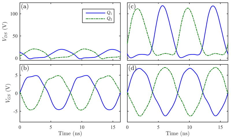
We measured the VDS and VGS of both CMCD FETs using a DSO6054a oscilloscope from Agilent Technologies and P6158 low capacitance probes from Tektronix. Figure 4 (a) and (b) show VDS and VGS at RFREF=+3 dBm, while (c) and (d) show VDS and VGS at RFREF=+17 dBm. The 500 MHz bandwidth limit of the oscilloscope significantly distorts the VDS waveforms to the extent that ZVS cannot be accurately observed. Because of this, the fine tuning of the CMCD output tank was done based on maximizing efficiency near maximum output power.
Figure 4.
Measured operating waveforms of the CMCD stage.
The observed phase offset and amplitude of the VGS waveforms change significantly with power level. The apparent increase in VGS amplitude is due to parasitic inductance between the RF probe’s ground and the eGaN FET’s true source connection. The change in phase offset between VGS of the two FETs is not a measurement artifact, and is due to asymmetric AM-PM distortion in the two preamplifier chains. In practice, component values in class E preamplifiers’ matching circuits were empirically adjusted so that the phase offset was 180° at maximum power.
Frequency domain
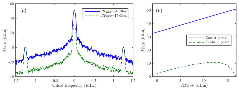
Since the class S amplifier is a switching DC-DC converter, VB will contain some ripple voltage which will modulate the RFPA’s output. The result is sidebands in the output spectrum at offset frequencies equal to the switching frequency of the class S amplifier (1.25 MHz and its harmonics). This is potentially problematic for MRI, as these sidebands may cause unwanted excitation of spins whose signal may contaminate the acquired images. In order to observe these sidebands, we connected the module’s output to a signal analyzer (Agilent N9000A) via the broadband 50 Ω attenuator. The module output 20 ms pulses with varying RFREF power between −1 dBm and +17 dBm. The SA was configured with a frequency span of 3 MHz and a readout bandwidth (RBW) of 39 kHz. The SA was set to trigger on the RF pulse with 100 μS of trigger delay, and eight pulses were averaged at each power level. Figure 5 (a) shows the acquired spectra for RFREF power levels of −1 dBm and +17 dBm. Figure 5 (b) shows the carrier and sideband power vs input power.
Figure 5.
(a) Spectra of the RFPA output (b) Output carrier and sideband power vs input power
The sideband power peaks at roughly +12 dBm, which corresponds to the class S amplifier operating near 50% duty cycle. Those familiar with DC-DC converters will find this unsurprising, as the ripple current of a buck converter in continuous conduction mode is maximized at D=50% (31). The ratio between the carrier and sideband is maximized at the maximum power level (50.6 dBc at RFREF=+17 dBm) and was minimized as input power approached its minimum (31.5 dBc at RFREF=−1 dBm).
In a simple slice-selective excitation, the sidebands will excite extra slices at offset given by:
| (1) |
For ɏ=42.57 MHz/T and fSB=1.25 MHz and GS= 70 mT/m, the slice offset is 42 cm, which is outside the FOV of typical 3D imaging sequences. So long as the slice is outside the FOV, its signal should be be filtered out by the receive chain, resulting in no contamination. In the case of applications where out-of-FOV excitation is required, such as labelling in ASL (32), the sidebands may be mitigated by increasing the switching frequency of the class S amplifier or adding frequency dithering to the PWM controller.
Static nonlinearity and efficiency
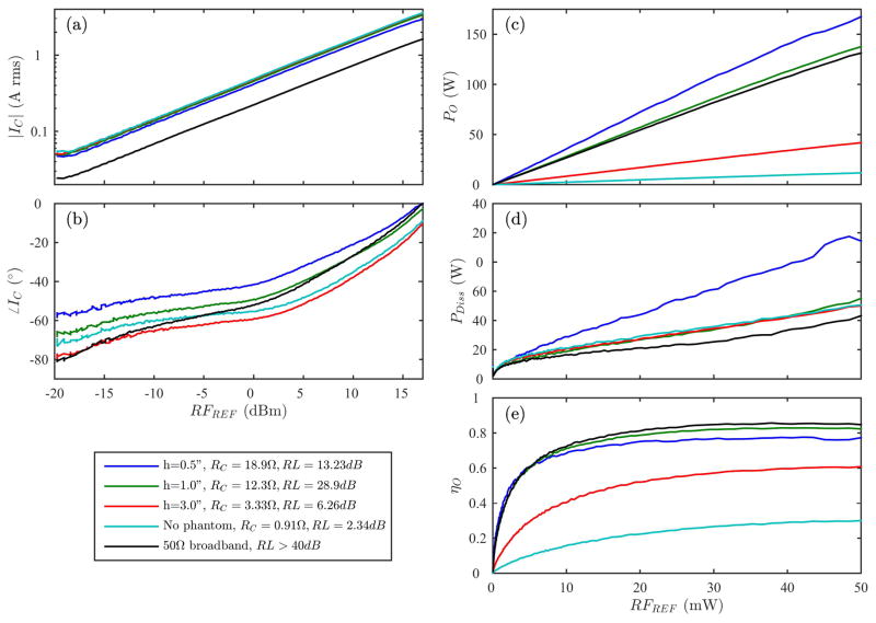
Figure 6 shows the results of all five experiment iterations. Figure 6 (a) and (b) show the magnitude and phase of the RF output as a function of RFREF power. The output magnitude is very linear with respect to the RFREF for input levels above −19 dBm. Below this point, the RF output power reaches a minimum due to the class S amplifier reaching its minimum on-time of 10 ns. Thus the dynamic range ratio of the module’s output power is 36 dB. There is also AM-PM distortion across the full power range. The AM-PM distortion at low power is due to the gate drive feeding through directly to the RF output via the CRSS of the eGaN FETs. The AM-PM distortion at higher power is due to the nonlinearity of COSS vs VB.
Figure 6.
Measured output magnitude (a), phase (b), power (c), dissipated power (d), and efficiency (e) of the RFPA module output vs RFREF power.
The measured fundamental output power PO and dissipated power PDiss, as defined according to (2), are plotted in Figure 6 (c) and (d). Figure 6 (e) shows the overall efficiency ηO for each experiment, defined according to (3). PDC is the bias power to the RFPA, and PQ is the quiescent power consumed by the rest of the module in the active state (2.05 W). The attenuation of the λ/2cable feeding the coil is given by α, and was measured at −0.227 dB.
| (2) |
| (3) |
The experiment using the broadband 50 Ω load showed a maximum η0 near 85% and a maximum load power of 131 W. When driving a matched coil load at h=1″, the maximum η0 was near 83% and the maximum PO was 138 W. When h is increased or the phantom is removed, the resulting coil current only increases slightly due to amplifier decoupling provided by the impedance matching network. PDISS also changes very little under light load conditions. This implies that the CMCD stage does not dissipate reflected power from a mismatched load.
While light load conditions do not present a problem to the module, increasing the loading by decreasing h below the optimal h=1″ distance caused the load power and dissipated power to increase substantially. At h=0.5″ η0 drops to 77% while dissipated power increases to nearly 50 W. Therefore when using such an impedance transformer, it is recommended to tune and match the coil to give an optimal match at the maximum expected loading condition.
We also repeated these measurements for frequency offsets up to Δf = ±1 MHz with the broadband 50 Ω load and found that PO and ηd varied by up to 12% and 1.5% over that range, respectively. However for a narrowband load PO an ηd will degrade for large Δf, depending on the Q of the coil. When driving a tuned RF coil, the operating frequency range of the RFPA module will tend to be limited by the coil’s bandwidth and not the RFPA.
Thermal performance
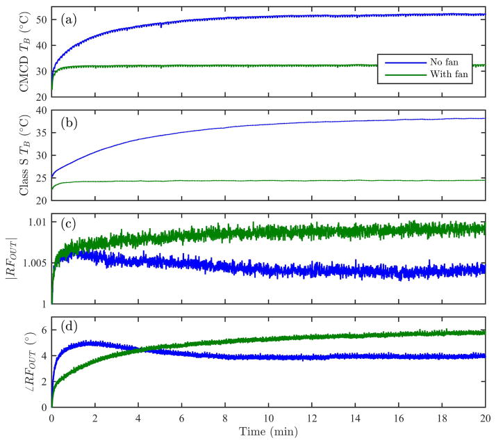
Figure 7 shows the results of the thermal drift experiment with and without forced air cooling.
Figure 7.
Results of 20 minute thermal performance experiment. (a) Measured board temperature near CMCD FETs. (b) Measured board temperature near class S FETs. (c) Normalized magnitude of RF output. (d) Normalized phase of RF output.
Based on the measured board temperatures TB, power dissipation, and ambient temperature (TA=22 °C) we calculated the steady state board to ambient thermal impedance RθBA and the 90% thermal rise time tr(BA) of each stage, both with and without forced air cooling. We also used the transient thermal impedance data provided by EPC and the measured power dissipation to estimate the maximum junction to board temperature rise ΔTJB, and thus the peak absolute junction temperatures TJ. Based on previous measurements, it was assumed that 75% of the total power dissipation was spread evenly between the two CMCD FETs, while the other 25% was in the upper FET of the class S stage. The results of this analysis are given in Table 2.
Table 2.
Summary of thermal performance of the RFPA module with and without forced air cooling.
| Fan | ΔTBA (°C) | Average Dissipation (W) | RθBA (°C/W) | tr(BA) (sec) | Peak TJ (°C) | |||||
|---|---|---|---|---|---|---|---|---|---|---|
| CMCD | Class S | CMCD | Class S | CMCD | Class S | CMCD | Class S | CMCD | Class S | |
| No | 29.7 | 15.8 | 1.34 | 0.45 | 22.1 | 35.2 | 349 | 550 | 78.2 | 51.1 |
| Yes | 10.0 | 2.1 | 1.31 | 0.44 | 7.6 | 4.7 | 40.6 | 181 | 57.8 | 37.1 |
Drift in the RF output is also of concern for this application. Figure 7 (c) and (d) show the RF output magnitude and phase, respectively. These measurements are normalized to the initial value of each experiment. The magnitude of the RF output is seen to only drift up to 1%, but phase drift causes the overall error vector to drift by up to 11%.
Imaging experiment
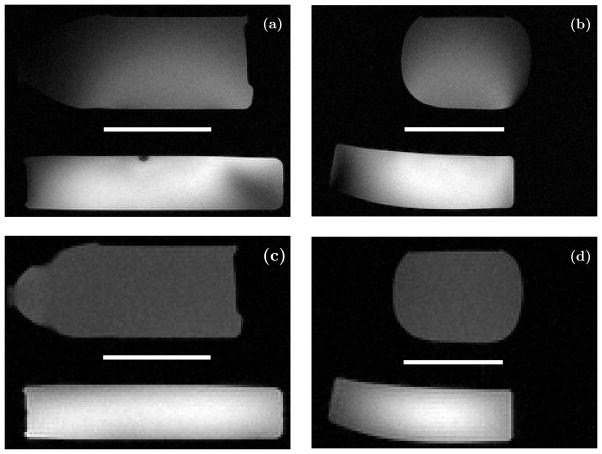
Figure 8 (a) and (b) show images of the oil and water phantoms taken while using the RFPA for transmit and the body coil for receive. Figure 8 (c) and (d) were acquired using the body coil for both transmit and receive. The TX coil and RFPA module were present in the bore during all acquisitions. No artifacts aside from the expected B1 inhomogeneity were associated with the presence of the RFPA module.
Figure 8.
Transverse (a) and sagittal (b) images using the RFPA module. (c) and (d) show reference images using the body coil. The white line in the center indicates the location of the TX coil.
Discussion
Here we have demonstrated an improved RFPA module based on the CMCD topology with GaN FETs operating at 123.25 MHz. The module was tested with a maximum output power of 130 W into an unbalanced 50 Ω port with an overall efficiency of up to 85%. This is as compared to the original module which drove a coil directly with a maximum output power of 40 W with ηO=80% (21). We also demonstrated that when operated near its maximum output power with a duty cycle of 10%, the peak junction temperature TJ of the eGaN FETs remained under 80 °C, even when only relying on the PCB for heat transport in still air. The use of forced air convection on the module further reduced the peak TJ to 58 °C. In the case that forced cooling is necessary to protect the amplifiers, the amplifiers must be protected in the case where the cooling system fails. A simple watchdog circuit should utilize the thermistors in order to inhibit the amplifiers when the board temperature rises beyond a safe threshold. In the future we aim to implement digital telemetry for status monitoring of each module.
The overall size of the module was 13.5 cm × 4.3 cm × 3.5 cm. All components, with the exception of the toroidal chokes, the output balun, and the printed circuit boards are available off the shelf, with an estimated bill of materials under $120 (in quantities of 1000). The power amplifiers themselves only contribute a small fraction of the overall size and cost of the module. These results suggest that even higher average power density could be yielded from the EPC2012C at 123 MHz. Large gains in output power capacity could likely be realized by using larger 200V eGaN FETs, such as the EPC2019 and EPC2010C.
The module does not rely on ferrite or powdered iron magnetic components, or any other ferrous materials, for its operation. However many components do contain ferrous plating in their packaging and leads, most notably in ceramic capacitors, many of which may be replaced with nonmagnetic equivalents at greater cost (33).
Imaging experiments demonstrated the use of two modules as in-bore RFPAs to obtain different excitation profiles. The presence of the modules within the bore did not produce any noticeable artifacts in the images. Future work will aim to operate all 16 channels of the array using the modules, and utilize predistortion to correct for nonlinearity and coupling between channels. The primary challenge associated with the CMCD topology is control of coil current. The module shows significant AM-PM distortion which arises from the capacitances in the eGaN FETs. Additionally, the dynamic range of the class S amplifier was limited to 36 dB, mainly due to the minimum pulse width of the gate driver. We also observed drift in the phase of the RF ouput due to temperature drift. All of these effects may be mitigated by use of minimum envelope roughness techniques as proposed by Grissom et al (34). Model-based predistortion (8) or iterative feedback methods (9,10) would likely be necessary for adequate control of coil current. A more ambitious approach would be to use real-time complex feedback methods such as cartesian (11,13) and polar (23) feedback.
The high power efficiency of the RFPA module will be beneficial for anatomy-specific local pTX systems requiring high channel counts. Thermal management is greatly simplified, and the size of the amplifiers can be reduced compared to linear class RFPAs, allowing them to be located inside the magnet bore. This would greatly decrease the need for RF power cabling, which is a significant driver of cost in pTX systems. It is also plausible that high efficiency modules would be suitable for full body pTX arrays, with the amplifiers located just outside the scanner bore.
Acknowledgments
This work received research support from Siemens and NIH 5R01-EB016728. We would also like to thank Bhairav Mehta for assistance during the imaging experiment.
References
- 1.Sotgiu A, Hyde JS. High-order coils as transmitters for NMR imaging. Magnetic Resonance in Medicine. 1986;3(1):55–62. doi: 10.1002/mrm.1910030108. [DOI] [PubMed] [Google Scholar]
- 2.Van de Moortele P, Akgun C, Adriany G, Moeller S, Ritter J, Collins CM, Smith MB, Vaughan JT, Uğurbil K. B1 destructive interferences and spatial phase patterns at 7 T with a head transceiver array coil. Magnetic Resonance in Medicine. 2005;54(6):1503–1518. doi: 10.1002/mrm.20708. [DOI] [PubMed] [Google Scholar]
- 3.Webb AG, Collins CM. Parallel transmit and receive technology in high-field magnetic resonance neuroimaging. International Journal of Imaging Systems and Technology. 2010;20(1):2–13. [Google Scholar]
- 4.Homann H, Graesslin I, Eggers H, Nehrke K, Vernickel P, Katscher U, Dössel O, Börnert P. Local SAR management by RF shimming: a simulation study with multiple human body models. Magma (New York, NY) 2012;25(3):193–204. doi: 10.1007/s10334-011-0281-8. [DOI] [PubMed] [Google Scholar]
- 5.Eryaman Y, Guerin B, Akgun C, Herraiz J, Martin A, Torrado-Carvajal A, Malpica N, Hernandez-Tamames JA, Schiavi E, Adalsteinsson E, et al. A Simulation Based Validation of a pTx Pulse Design Strategy Using Implant-Friendly Modes for Patients with DBS Implants. 22nd ISMRM; Milan, IT. 2014. [Google Scholar]
- 6.Gudino N, Sonmez M, Faranesh A, Lederman R, Balaban R, Hansen M, Griswold MA. Parallel transmit excitation at 1.5 T based on the minimization of a driving function for device heating. 21st ISMRM; Salt Lake City, UT. 2013. [DOI] [PMC free article] [PubMed] [Google Scholar]
- 7.McElcheran C, Golestanirad L, Graham S. Reduced Heating of Implanted Electrical Conductors Using Parallel Radiofrequency Transmission. 22nd ISMRM; Milan, IT. 2014. [Google Scholar]
- 8.Raab FH. High-Efficiency RF Power-Amplifier Module for Magnetic-Resonance Imaging. Montreal: 2011. [Google Scholar]
- 9.Stang PP, Kerr A, Grissom W, Pauly JM, Scott GC. Vector Iterative Pre-Distortion: An Auto-calibration Method for Transmit Arrays. 17th ISMRM; Honolulu, Hawaii, USA. 2009. [Google Scholar]
- 10.Zhu K, Dougherty RF, Middione MJ, Wu H, Scott G, Pauly JM, Kerr AB. RF Amplifier Nonlinearity Correction for Multiband RF Pulses. 23rd ISMRM; Toronto CA. 2015. [Google Scholar]
- 11.Hoult DI, Kolansky G, Kripiakevich D, King SB. The NMR multi-transmit phased array: a Cartesian feedback approach. Journal of Magnetic Resonance. 2004;171(1):64–70. doi: 10.1016/j.jmr.2004.07.020. [DOI] [PubMed] [Google Scholar]
- 12.Gudino N, Heilman JA, Riffe MJ, Heid O, Vester M, Griswold MA. On-coil multiple channel transmit system based on class-D amplification and pre-amplification with current amplitude feedback. Magnetic resonance in medicine. 2013;70(1):276–289. doi: 10.1002/mrm.24462. [DOI] [PMC free article] [PubMed] [Google Scholar]
- 13.Zanchi MG, Stang P, Kerr A, Pauly JM, Scott GC. Frequency-Offset Cartesian Feedback for MRI Power Amplifier Linearization. IEEE Transactions on Medical Imaging. 2011;30(2):512–522. doi: 10.1109/TMI.2010.2087768. [DOI] [PMC free article] [PubMed] [Google Scholar]
- 14.Kurpad KN, Wright SM, Boskamp EB. RF current element design for independent control of current amplitude and phase in transmit phased arrays. Concepts in Magnetic Resonance. 2006;29B(2):75–83. [Google Scholar]
- 15.Chu X, Yang X, Liu Y, Sabate J, Zhu Y. Ultra-low output impedance RF power amplifier for parallel excitation. Magnetic Resonance in Medicine. 2009;61(4):952–961. doi: 10.1002/mrm.21908. [DOI] [PMC free article] [PubMed] [Google Scholar]
- 16.Vaughan JT, Myer D. RF Coil Element Mounted Power Amplifiers. 19th ISMRM; Montréal Québec, CA. 2011. [Google Scholar]
- 17.Kurpad KN, Boskamp EB, Wright SM. Eight channel transmit array volume coil using on-coil radiofrequency current sources. Quantitative Imaging in Medicine and Surgery. 2014;4(2):71–78. doi: 10.3978/j.issn.2223-4292.2014.04.14. [DOI] [PMC free article] [PubMed] [Google Scholar]
- 18.DelaBarre L, Myer D, Vaughan JT. Muti-Channel, In-bore Power Amplifiers for Multi-channel Coil at 7T. ISMRM; Salt Lake City, UT. 2013. [Google Scholar]
- 19.Heilman J, Riffe MJ, Oliver H, Griswold MA. High power, high efficiency on-coil current-mode amplifier for parallel transmission arrays. 15th ISMRM; Berlin. 2007. [Google Scholar]
- 20.Kahn L. Single-Sideband Transmission by Envelope Elimination and Restoration. Proceedings of the IRE. 1952;40(7):803–806. [Google Scholar]
- 21.Twieg M, Riffe MJ, Gudino N, Griswold MA. Enhancement Mode GaN (eGaN) FETs for On-Coil MRI Transmit Amplifiers. 21st ISMRM; Salt Lake City, UT. 2013. [Google Scholar]
- 22.Bernstein MA, King KF, Zhou ZJ. Handbook of MRI pulse sequences. Amsterdam; Boston: Academic Press; 2004. p. 1017. [Google Scholar]
- 23.Reynaert P, Steyaert M. RF Power Amplifiers for Mobile Communications. Springer; 2010. [Google Scholar]
- 24.Stang PP, Pauly JM, Scott GC. A High-Efficiency Linear MRI Transmit Amplifier using Envelope-Tracking. 21st ISMRM; Salt Lake City, UT. 2013. [Google Scholar]
- 25.Kobayashi H, Hinrichs JM, Asbeck PM. Current-mode class-D power amplifiers for high-efficiency RF applications. IEEE Transactions on Microwave Theory and Techniques. 2001;49(12):2480–2485. [Google Scholar]
- 26.Lidow A, editor. GaN transistors for efficient power conversion: the eGaN FET journey continues. El Segundo, CA: Power Conversion Publications; 2012. p. 208. [Google Scholar]
- 27.Twieg M, Griswold MA. Optimizing the Current-Mode Class D (CMCD) Amplifier for Decoupling in pTX Arrays. 23rd ISMRM; Toronto CA. 2015. [Google Scholar]
- 28.Venable Industries. Venable Technical Paper #3, Optimum Feedback Amplifier Design For Control Systems. [Google Scholar]
- 29.Twieg M, Griswold MA. Large-Signal Characterization of Coupled RF Amplifiers for Parallel Transmit. 22nd ISMRM; Milan, IT. 2014. [Google Scholar]
- 30.Reykowski A, Wright SM, Porter JR. Design of matching networks for low noise preamplifiers. Magnetic Resonance in Medicine. 1995;33(6):848–852. doi: 10.1002/mrm.1910330617. [DOI] [PubMed] [Google Scholar]
- 31.Billings KH, Morey T. Switchmode power supply handbook. 3. New York: McGraw-Hill Professional; 2011. p. 1. [Google Scholar]
- 32.Alsop DC, Detre JA, Golay X, Günther M, Hendrikse J, Hernandez-Garcia L, Lu H, MacIntosh BJ, Parkes LM, Smits M, et al. Recommended implementation of arterial spin-labeled perfusion MRI for clinical applications: A consensus of the ISMRM perfusion study group and the European consortium for ASL in dementia. Magnetic Resonance in Medicine. 2015;73(1):102–116. doi: 10.1002/mrm.25197. [DOI] [PMC free article] [PubMed] [Google Scholar]
- 33.VJ Non-Magnetic Series for IR Reflow Soldering. 2016.
- 34.Grissom WA, Kerr AB, Stang P, Scott GC, Pauly JM. Minimum Envelope Roughness Pulse Design for Reduced Amplifier Distortion in Parallel Excitation. Magnetic Resonance in Medicine. 2010;64(5):1432–1439. doi: 10.1002/mrm.22512. [DOI] [PMC free article] [PubMed] [Google Scholar]


