

Colors of materials are precisely laser-controlled using new manufacturing technology with nanopatterned semiconductor surfaces.
Keywords: laser-printing, structural colors, metasurfaces, high-index dielectrics, resonators, super-resolution
Abstract
Man-made structural colors, which originate from resonant interactions between visible light and manufactured nanostructures, are emerging as a solution for ink-free color printing. We show that non-iridescent structural colors can be conveniently produced by nanostructures made from high-index dielectric materials. Compared to plasmonic analogs, color surfaces with high-index dielectrics, such as germanium (Ge), have a lower reflectance, yielding a superior color contrast. Taking advantage of band-to-band absorption in Ge, we laser-postprocess Ge color metasurfaces with morphology-dependent resonances. Strong on-resonance energy absorption under pulsed laser irradiation locally elevates the lattice temperature (exceeding 1200 K) in an ultrashort time scale (1 ns). This forms the basis for resonant laser printing, where rapid melting allows for surface energy–driven morphology changes with associated modification of color appearance. Laser-printable high-index dielectric color metasurfaces are scalable to a large area and open a new paradigm for printing and decoration with nonfading and vibrant colors.
INTRODUCTION
Optical metasurfaces (1, 2) provide new means for manipulation of optical fields with the aid of structural resonances and/or artificial birefringence that can alter amplitude, phase, and polarization over subwavelength distances (3–5). Metasurfaces are harvested from subwavelength structures that are metallic (6–9), dielectric (10–18), or hybrid combinations (19–22). Color metasurfaces generated from resonant interactions between visible light and the nanoscale surface textures are highly desired for ink-free color decoration. Thin-film interference at metasurfaces with absorbing materials has been used for color patterning (23–25), although it is inherently limited in its spatial resolution. In contrast, plasmonic color metasurfaces (26–28) have been printed with subwavelength resolution (29–32), whereas structural colors caused by the composition of low-index dielectric materials require long-range orders (33, 34), thus posing a challenge for high-resolution, large-area, and non-iridescent applications of all-dielectric color metasurfaces.
All-dielectric structures form the basis for a rich palette of structural color phenomena in nature (35, 36), and artificial colors can also be supported by carefully engineered and nanofabricated high-index dielectric surfaces (37, 38), for example, localized resonances in dielectrics (39), such as silicon (Si) nanostructures (40–43). At the same time, there is also a tremendous attention to plasmonic structural colors (28, 44), where colors develop when ultrathin metal films are evaporated onto pre-nanostructured polymer substrates, such as large arrays of polymer nanopillars (29, 32, 45). Here, we describe how essentially similar mass production approaches (46) can also be used for all-dielectric color metasurfaces by substituting metal coatings with high-index dielectric films, such as semiconductor materials.
RESULTS
A schematic representation of the structures is provided in Fig. 1A, where a thin film of germanium (Ge) is deposited on a substrate with nanoimprinted polymer pillars. In this way, dielectric disks can be raised above a same-thickness dielectric film representing an inverse of the disk array, that is, a high-index dielectric film with “holes” penetrated by low-index pillars. We note that both disks and holes inherit their common topology from the polymer pillars, and thus, one can also make other cross sections, such as bars. Ge was selected in the initial applications because of its high refractive index and because it comprises some attenuation at visible frequencies, which is essential for the ultimate color generation and laser printing that we describe. In particular, abundant high-index materials can be used for these structural color generations, which are multifunctional and potentially environment-inert (see also the results with Si in fig. S1) (47–51). Here, polymer substrates were preferred because of their flexibility, ease of fabrication, and throughput scale-up in nanoimprint lithography. Optically transparent polymers (here, Ormocomp is considered) can further enhance the color visibility and, at the same time, isolate the laser-induced heating within the on-top lossy materials in the following laser printing processes. The scanning electron microscope (SEM) image of a small selected area of the nanostructures after Ge deposition is shown in Fig. 1B, illustrating the fixed periodicity P = 200 nm of the lattice and the radius R of the disks in our design. The interaction of light within the hybrid disk-hole structure can be enhanced markedly by trapping light with multiple total internal reflections. Dipole resonance conditions can be fulfilled for subwavelength structures that are made of high-index materials (40, 52–54). We note the remarkable property of weakly absorbing dielectric media, where at resonance, for example, Ge resonators can absorb significantly more light than those that intersect their physical cross sections. As a result, light can be absorbed by the spatially isolated (localized) disks when the incident light is spectrally aligned with the optical resonances supported by the nanostructures. Therefore, this results in a modified reflection spectrum and color appearance.
Fig. 1. Structural colors based on high-index dielectrics.
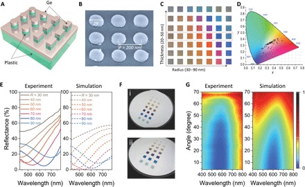
(A) Schematic demonstration of the structures. (B) A 45° side-angle SEM image of imprinted plastic structures after Ge deposition. Color information is shown to clarify the diameter and spacing of the nanopillar structure. (C) Full palette of colors is revealed in an array of squares. By varying the radius of the pillars and the deposited Ge film thickness, structures with the same periodicity display a wide range of colors (from bottom right to top left). The highlighted row was measured to produce the experimental reflection spectra in (E). (D) Experimental structural color gamut of measured reflectance spectra from color plates in (C) presented in a standard CIE-1931 color space. (E) Selected experimental and simulated spectra for Ge films with a thickness T = 35 nm. The dips shift to longer wavelengths with varying radius of the nanostructures from R = 30 to 90 nm. (F) Taken at (i) normal and (ii) 60° side angle, optical images of an imprinted 10 cm sample following deposition of thin Ge layers with a uniform thickness T = 40 nm, showing the color rendition of 5 mm–by–5 mm squares similar to the third row in (C). (G) Experimental and simulated reflection spectra for angles of incidence from 4° to 70° for a sample with T = 35 nm and R = 75 nm (reflectivity is indicated by color bars).
Subwavelength localization of light is naturally provided by plasmonic nanostructures (55), whereas high–refractive index dielectrics may also manipulate light on length scales beyond its wavelength (39, 56, 57). The resonant wavelengths in high-index dielectric cavities intuitively follow the picture of whispering gallery–like modes, where the effective wavelength of the trapped light is related to the geometry of the cavities. Here, we note an important difference with plasmonic structures that share the same overall geometry (45), whereas the dielectric film is replaced by a metallic film. In the plasmonic case, localized disk resonances hybridize through near-field coupling with hole plasmon resonances that are also spatially localized (32), that is, with a mutual spatial overlap. On the other hand, in our dielectric case, the holey film acts as a void-type slab photonic crystal (58), with delocalized low-frequency states predominantly occupying the high-index region of the layer while hardly penetrating into the low-index hole regions. Consequently, disk modes have a modest field overlap with modes in the photonic crystal film, and the response can largely be understood from the disk dipole modes supported by the array of dielectric disks. In addition to electric dipole resonances, magnetic dipole resonances can also be supported in these structures (59–61). This property makes the high-index dielectric resonators a diverse system with additional degrees of freedom. For example, by controlling the height and radius of the disk, one may achieve tunable double-resonance characteristics (61), a property that may help further improve the spectral response and, in turn, the color appearance. For the realization of large-area metasurfaces, these dielectric nanoparticles can be printed onto surfaces using laser-based methods (62), whereas we lean against approaches developed for the production of plasmonic color metasurfaces (32, 46).
By systematically varying the disk parameters, such as the disk radius R and the film thickness T (while keeping the height of the pillar H = 60 nm fixed), we achieve a full palette of colors that span the visible range, as shown in Fig. 1C. Figure 1D shows the related color gamut of these color palettes in a standard CIE-1931 color space. Although the colors are not at the edges, they still cover most of the color space for traditional laser color printers. The measured reflection spectra for Ge films of thickness T = 35 nm coated on the pillars with R = 30 to 90 nm are shown in Fig. 1E (left), demonstrating broadband absorption resonances, with the spectral position determined by the radius of the disks. The wide optical absorption band creates the high-contrast color by suppressing a portion of the reflectivity in the visible spectrum down to the 5% reflection level. The corresponding simulated reflection spectra are shown in Fig. 1E (right), showing qualitative agreement with the experimental results. It should be mentioned here that one particular challenge of plasmonic colors relates to vibrancy, in which all-dielectric nanostructures are potentially supporting resonances that are narrower than plasmonic counterparts, where ohmic loss gives some inherent limitations to the resonance quality factor (63). In this context, Ge represents an alternative, where the homogeneous broadening of resonances is acceptable, whereas there is sufficient above-bandgap absorption for the laser heating to work effectively (fig. S2). Moreover, a protective coating will slightly redshift the resonances in our system, thereby causing a relatively small color change as a result of the increased surrounding refractive index (fig. S3). To appreciate the importance of localized resonances within the subwavelength structures, we preserved the optical properties with respect to the angle of light incidence. Figure 1F shows images of a sample taken at normal and large oblique angle luminescence. Because the resonators are smaller than the wavelength of light, the supported localized resonances ensure that the reflected colors from these structures are robust with respect to the angle of incidence. We further demonstrated this by measuring and simulating the angle-resolved reflectivity of a sample, showing that the absorption feature remains prominent for angles of incidence from normal incidence up to 60° (see Fig. 1G).
In addition to the structure-generated static colors, there is also an interest in postprocessing and dynamical reconfiguration of colors (48, 64–66). Plasmon resonances in metal nanostructures offer the capability of confining the optical excitation far beyond the diffraction limit (55, 67). This can be used to greatly enhance the photothermal effect (68), and it was explored for plasmonic color laser printing, where plasmonic heating locally melts and reconfigures the metallic nanostructures (69). Obviously, plasmonic heating is closely linked to field confinement at metal surfaces, with limited access to structural melting that emerges from a material’s bulk response. Furthermore, plasmonic resonances may also provide the particles with a repulsive momentum from the surface (70), leading to a random offset of the particles at printing (69, 71). In optical heating, the absorbed heat power density reflects the electric field distribution E in the resonator, that is, qabs = ½ωε″|E|2, where ω is the angular frequency and ε″ is the imaginary part of the dielectric function ε = ε′ + iε″ of the resonator material. Optically, because they are largely transparent at the frequencies of interest, dielectrics differentiate themselves from metals. Hence, we usually associate dielectrics of high optical quality with ε′ ≫ ε″ ≅ 0. In this aspect, semiconductors, such as Si and Ge, are high-index dielectrics with ε′ ≫ 1, whereas above-bandgap absorption provides a significant damping in the visible region, where ε″ for Ge is comparable to that of Al in the visible region. Thus, we anticipate opportunities for localized dielectric heating and melting-induced morphology changes of Ge nanostructures, with possible parallels to plasmonic heating used for plasmonic color laser printing (69). Here, the more evenly distributed light energy in the dielectric resonators will potentially heat the resonator volumes more homogeneously. The associated heat-driven morphology changes might, in turn, be more controllable, thus allowing us to realize the long-standing goal of ink-free, high-speed, and subdiffraction full-color laser printing in an entirely dielectric material architecture.
Laser heating is generally of a random stochastic nature because of the complex thermodynamic phase transitions in the materials (72, 73). When the incident laser frequency is close to an optical resonance of the structure, the frequency coincidence (or resonance) can promote greatly enhanced absorption of electromagnetic energy, which facilitates the ultralow power consumption and frequency selectivity in laser printing. Consider a morphology-dependent optical resonance, which is resonantly driven by a pulsed laser. Because the resonance frequency depends critically on the detailed morphology of the resonator volume, the on-resonance pulsed laser should only provide a little energy dissipation to slightly change the morphology, that is, from an initially flat disk in the direction of a spherical shape, thus shifting the spectral response into an off-resonance state. The heating is consequently weakened, and morphology reshaping is discontinued (fig. S4). This optical resonance–based selectivity provides distinct power targets for generating identical structural colors by well-controlled photothermal reshaping processes, which offer easier color selection and halftoning. Figure 2A illustrates the setup for resonant laser printing (RLP) of structural colors. We used the selectivity of RLP to achieve resonance-mediated structural color printing governed by photothermal reshaping. Figure 2B presents the reflective and transmitted optical microscope images of the resulting colors, showing gradual color change from cyan to yellow when the applied laser irradiation with single nanosecond laser pulses is linearly increased (pulse energy of 0.2 to 1.8 μJ in the focal plane). We acquired SEM images after laser heating using different energy doses (Fig. 2C). The laser heating within the Ge resonators gives well-defined reshaping of structures, whereas plasmonic laser heating, as used recently for plasmonic color printing (69), might result in particles that are propelled away from the interface owing to the intense laser field and a rapid thermal change at the metal surface during the melting process (see also fig. S5). Figure 2D and 2E show the measured and simulated spectral data corresponding to each RLP in Fig. 2B (color squares). Spectral features blueshift as a result of the gradual decrease in the disks’ diameter. The related colors generated by RLP can cover cyan, magenta, and yellow (CMY) gamut, as represented in a CIE-1931 chromaticity diagram (Fig. 2F).
Fig. 2. Macroscopic RLP of structural colors.
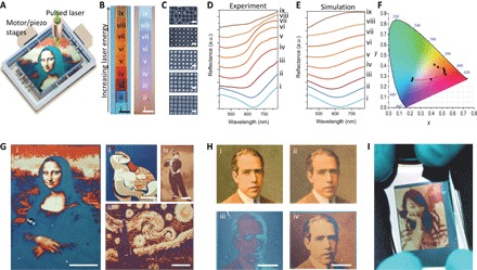
(A) Schematic setup of RLP. Synchronous motion solution with the laser pulses is provided by computer-controlled motor or piezo stages. (B) Reflection and transmission microimages of multicolored structures generated by gradually increasing laser powers. Microstructures (i to ix) are generated under gradually increasing laser power strengths from 0.2 to 1.8 μJ in steps of 0.2 μJ, controlled using a liquid crystal attenuator. Scale bars, 0.5 mm. (C) Corresponding SEM images of the microstructures (i, iii, v, vii, and ix) in (B), showing the change of the morphology of the unit cell from disk to sphere and eventually a hole. Scale bars, 200 nm. (D) Experimental reflection spectra of the corresponding laser-printed color squares in (B). Note that the dips (absorbed light) with varying printing laser powers blueshift, causing color changes from cyan to yellow. a.u., arbitrary units. (E) Corresponding simulated reflection spectra. (F) Gamut loop of laser-printed structural colors, which covers CMY colors. (G) Collection of laser-printed paintings with protective polymethyl methacrylate (PMMA) coating (sufficiently thick to suppress Fabry-Pérot interference) deposited before laser printing. Samples have R = 135 nm with deposited Ge film thicknesses T = 45 nm (i), 40 nm (ii), 35 nm (ii), and 30 nm (iv), respectively. Scale bars, 5 mm. (H) Image of a colorful portrait (i), CMY halftoning of the original image (ii), printing of halftoned magenta color onto the initial cyan background (iii), and laser-printed full-color CMY halftoned image (iv). Scale bars, 5 mm. (I) Structural color laser printing of a portrait image. CMY halftoning realizes red, brown, and especially a saturated black color.
To demonstrate the working principle of RLP, we printed several macroscopic images in various color tones, which are shown in Fig. 2G. All images are visible and can be recorded using a commercial camera (Canon EOS) (see also fig. S6). The color appearance and contrast demonstrate the feasibility of our RLP scheme on these ultrathin, flexible, and laser-printable metasurfaces that work as printable paper (see also fig. S7).
We also demonstrate the full CMY color halftoning abilities of our RLP approach, which is a normal component of traditional laser printers. The full capability of the structural color laser printing is exemplified in Fig. 2H by printing a colorful portrait of Niels Bohr. The original (Fig. 2H, i) and the corresponding CMY halftoning (Fig. 2H, ii) exhibit a mixture of all three base CMY colors. During the RLP process, the intensity of the magenta color is gradually tuned on the cyan background (Fig. 2H, iii). The final full-color printed portrait (Fig. 2H, iv) closely matches the original image (Fig. 2H, i). In most commercial ink-jet or laser printers, a black K (key) ink is also included, resulting in the CMYK color scheme. The K ink is needed for improving the image sharpness due to the imperfect transparency of commercially practical CMY inks. However, structural color printing processes almost never include a black component (which would imply total optical absorption) (45). For structural colors with high-index lossy dielectrics, the intrinsically large optical attenuation within the material leads to already strong resonant absorption (resulting in high-contrast colors) inside the structured films, which can be as thin as tens of nanometers. In our structural color laser printing processes, the printed CMY colors are almost perfectly reflective. A highly saturated CMY combination successfully leads to a halftoned black color, as shown in Fig. 2I. Our results have immediate implications for ink-free color decoration in industrial labeling and packaging, whereas we also anticipate its use for visual commodities, arts, and personal accessories with customized designs.
Super-resolution printing for color filtering has possible applications in retina displays for portable devices. We achieve a subdiffraction printing resolution of RLP, which is eventually limited by the lattice constant P of our metasurface. Our particular case with a 200-nm pitch translates into a resolution in excess of 120,000 dots per inch (DPI), with a corresponding pixel that is up to 500-fold smaller than the cross section of a human hair. We now discuss how we address a single resonator in our RLP (see Fig. 3A). The resolution of a traditional microscope used in laser printing (based on a lens for visible light) is limited by diffraction to ~λ/2 NA, where, in our case, λ = 532 nm, NA is the numerical aperture, and NA ≤ 0.85 (Fig. 3A, i). RLP easily exceeds the diffraction limit of conventional optical microscopy. The localized resonators provide a large field enhancement (Fig. 3A, ii) and a periodical redistribution of the optical energy densities by confining the optical energy within the high-index volumes (with high density of optical states), which are far beyond the diffraction limit. This spatial power enhancement and modulation of the Gaussian-like beam allows an effective printing area with a subdiffraction limited scale because of a threshold in the energy that is needed to drive morphology changes (Fig. 3A, iii). Thus, we can print an ultimate structural color pixel by only addressing the resonator associated with a single unit cell, whereas the energy dissipated in neighboring unit cells would not exceed the threshold for morphology changes (see Fig. 3B and fig. S8). To demonstrate the subdiffraction resolution color laser printing capability, we drew massive patterns on samples with T = 35 nm and R = 70, 80, and 90 nm. Figure 3C shows a collection of images printed with a subdiffraction resolution of 127,000 DPI. RLP was carried out at a speed of 1 min per image (only limited by the translation of the mechanical stage; see also movie S1). The images (with 62,500 pixels) are 50 μm by 50 μm each, which are even smaller than a single pixel of the latest Retina HD Display technology (63 μm). With cutting-edge RLP technology, the homogeneous field distribution of resonances inside the particles makes it possible to rapidly heat and modify these nanostructures with incredible accuracy. As shown in the SEM image in Fig. 3D, our RLP of the Parthenon temple discloses the laser-printed subdiffraction features that are beyond the reach of traditional microscopes. Figure 3E shows a high-magnification image (subarea with fine features indicated in Fig. 3D), illustrating the morphology transition of each particle due to the single–unit cell laser printing.
Fig. 3. Mechanism and result of the super-resolution RLP.
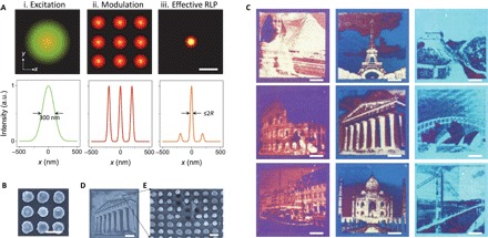
(A) Mechanism of the formation of a focal spot by overlapping the excitation beam and the periodical resonator array. A Gaussian excitation beam with low power (i) is enhanced and modified by the periodical resonators supporting highly confined localized resonances (ii), producing an effective photothermal heating area smaller than a diffraction-limited spot (iii). Scale bar, 200 nm. The original laser power for super-resolution printing should not exceed the threshold for melting an unstructured Ge thin film, whereas the locally enhanced energy density should overcome the threshold to initialize photothermal reshaping processes. (B) SEM image shows the RLP within a single unit cell, addressing the morphology change of the centered particle. Scale bar, 200 nm. (C) RLP images with a resolution of 127,000 DPI. The samples are with T = 35 nm and R = 70 nm (left), 80 nm (middle), and 90 nm (right), respectively. Scale bars, 10 μm. (D) SEM image of an RLP image in (C), which shows details of the structure and the corresponding electron scattering changes induced by laser printing. Scale bar, 10 μm. (E) SEM image of an enlarged region of the image in (D), showing the remarkable detail and morphology change on a single–unit cell level. These modified unit cells exhibit different colors in the optical image because of an RLP-induced variation in nanodisk sizes and the ablation of the disks. Scale bar, 200 nm.
To highlight the potential for future applications, particularly for three-dimensional display or encryption purposes (74), we used a polarization-sensitive color palette to create complex images by RLP at resolutions beyond the diffraction limit. By elongating the disks into bars (Fig. 4A), we show that the asymmetric structures can support tunable color under polarized incident light in the visible spectrum, in a similar manner to plasmonic structures (74, 75). When the local cylindrical rotational symmetry is lifted, the response of our electric and magnetic dipole modes becomes polarization-dependent, and colors can be switched continuously through polarization tuning (Fig. 4B). The application of RLP to asymmetric structures can easily render asymmetric resonators into morphologies of higher symmetry, that is, bars into spheres, because the latter are favored by a lower surface energy. The transition from Ge bars to spheres and eventual ablation (Fig. 4C) offers new degrees of freedom for structural color applications (fig. S9). Examples of laser-printed patterns with polarization-dependent color appearances are shown in Fig. 4D. These patterns have been printed with a resolution of 100,000 DPI (limited by the unit cell of 250 nm by 250 nm). Polarization-dependent laser printing allows for the encoding or hiding of color information within a single layer of structured surface (movie S2). By varying the Ge film thickness (here, T = 30 nm), we can modify the polarization-dependent optical responses of the laser-printed structures, making the optical resonances of transverse modes for bars, shortened bars, spheres, and holes located at the same frequencies, resulting in the same color printings. As shown in Fig. 4E, the printed pattern vanishes within the brownish background when the surface is illuminated by 90° polarized light, because all resonances produce colors that resemble the current color of the background (movie S3). We believe that RLP of a full-color high-resolution image, which can markedly change its appearance under orthogonal polarization illuminations, may pave the way for new functional color displays, security labels, and optical data storage applications.
Fig. 4. Polarization-sensitive RLP color generation.
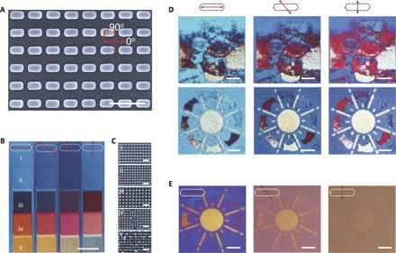
(A) SEM image of bar-hole structure shows the geometry parameters for polarization-sensitive RLP color generation. The dimensions of the long and short axes and the heights of the plastic pillars are 90, 55, and 50 nm, respectively. By varying the deposited Ge film thickness, we can still tune the color appearances and the strength of the polarization-dependent optical responses. Inset shows the polarization information, where the 0° polarized light field will excite the longitudinal mode along the long axis of the resonator, whereas the 90° polarized light field will excite the transverse mode along the short axis. Scale bar, 500 nm. (B) Optical images of color palettes printed by different laser power dosages illuminated under 0° to 90° polarized light. Note that switching in polarization-dependent colors is more feasible in low-power printed colors. Scale bar, 500 μm. (C) Corresponding SEM images of the laser-printed structures in (B), showing the gradual morphology change of the structures from bars to shortened bars and then to spheres and finally to holes. Scale bars, 200 nm. (D) Optical images of laser-printed pictures from a sample with Ge film thickness T = 45 nm illuminated under 0°, 45°, and 90° polarized light, respectively, showing polarization-sensitive colors. Scale bars, 10 μm. (E) Optical images of a laser-printed picture from a sample with Ge film thickness T = 30 nm illuminated under 0°, 45°, and 90° polarized light, respectively. Scale bars, 10 μm. The laser-printed pattern shows high color contrast under 0° polarized light but vanishes under 90° polarized light illumination.
CONCLUSIONS
In summary, we have demonstrated a unique structural color platform based on structured high-index dielectrics. Our realization of non-iridescent structural colors paves the way for a new class of materials for structural color generation, which are ultrathin, fully flexible, and environment-inert. In contrast to plasmonic heating, our work harvests from above-bandgap absorption, which represents the first applications of laser-printable structural colors with all-dielectric materials. With appropriately designed dielectric resonances, sufficient optical attenuation in the visible range allows resonant absorption of laser pulses. Thus, in practice, instantaneous heating and subsequent morphology relaxation of resonators allow ultrafast laser printing of full-color images with ultrahigh resolution. We demonstrate the high selectivity of printed colors by RLP, with examples of pure color printing and high-contrast CMY halftonings. Although we have used the visible absorption of Ge, RLP would also work with absorption bands beyond optical frequencies, whereas the “full” transparency of the visible band itself would facilitate even higher color vibrancy. Furthermore, we demonstrate the ultimate print resolution offered by RLP. Because of the subdiffraction spatial field modulation from the periodically arranged localized resonators, these structures enabled the printing of colors with a resolution exceeding 100,000 DPI, with the possibility for polarization-controlled colors. Our demonstrations open up new potential applications ranging from packaging and displaying to encryption, data storage, and retina devices.
MATERIALS AND METHODS
Sample preparation
To fabricate the Si master for nanoimprint, a resist-coated Si wafer was exposed by electron-beam lithography (JEOL JBX-9500FS 100 keV prototype) and then dry-etched. The Si stamp coated with an anti-stiction coating was used to replicate the pillar structure via room temperature nanoimprint into the Ormocomp layer. The Ormocomp film was cured by exposure to ultraviolet light, separated from the Si master, and peeled from the Borofloat glass substrate. Subsequently, a Ge film was deposited by an electron beam evaporator at 5 Å/s after imprint under a process pressure of ~10−6 mbar. A sufficiently thick layer of PMMA (10% 950PMMA in anisole, MicroChem Corp.) could be spin-coated on top to protect the samples.
Optical setups
The optical setup for laser color printing comprised a Nikon Ti-U inverted microscope, where a laser (CryLaS FDSS532-150) emitting 1-ns pulses at 532 nm was used for printing. The laser pulse energy was controlled and rapidly modulated with a liquid crystal attenuator. The sample was mounted on a computer-controlled piezo nanopositioning stage (Mad City Labs Nano-H50 series piezoelectric stage, 0.1-nm resolution, 50-μm travel, XY axis), which was placed on a computer-controlled motor stage. The same optical setup was used for spectroscopic imaging and measurements by combining an imaging spectrometer with a grating of 300 g/mm (Andor Shamrock 303i and Newton 920 CCD with 256 × 1024 pixels). Optical micrographs were acquired using a Nikon Eclipse L200 microscope with a Nikon digital camera (DS-Fi1). Macrophotographs were taken using a commercial digital camera (Canon EOS Mark II series).
Numerical simulation
The optical response of our structures was simulated in a commercially available electrodynamic simulation package (CST microwave studio) using a finite element method for reflection spectra and field distributions of structures under different illumination conditions. To simulate the photothermal reshaping processes, we used a simplified model of the complex thermodynamic phase transition. Neglecting gravity, we varied the thickness of round-cornered disks (to the final spherical shape) while preserving the overall initial material volume of the disks. An EM-thermal cosimulation approach was further used to solve the coupled electromagnetic and heat transfer problems.
Supplementary Material
Acknowledgments
We thank former colleagues J. Clausen and E. Højlund-Nielsen for Si master fabrication and C. Vannahme for technical support during the early stages of the optical setups. We also thank J. Scheel for help with taking the macroscopic images and P. A. D. Gonçalves, C. Yi, and S. Link for fruitful discussions. We particularly thank D. Li for providing the source images for laser printing. Funding: This work was in part funded by the Danish International Network Programme with Israel, Danish Agency for Science, Technology and Innovation (grants 137000124B and 407000158B), Innovation Fund Denmark, grant agreement 57-2014-3 (HemoPoC), and by the European Union’s Horizon 2020 Research and Innovation programme, under grant agreements No. 665233 (ChromaVision) and No. 686165 (IZADI-NANO2INDUSTRY). Author contributions: X.Z. and A.K. conceived the concept of RLP. X.Z. fabricated the samples and implemented the experiments and simulations. U.L., N.A.M., and W.Y. analyzed the role of supported optical modes in the complex structures. A.K. and N.A.M. provided feedback on the experiments. All authors contributed to the writing of the manuscript. Competing interests: X.Z., N.A.M., and A.K. are inventors on a patent entitled “Photothermal modification of high index dielectric structures” (application no. EP16207500.6, Danmarks Tekniske Universitet, 30 December 2016). The authors declare that they have no other competing interests. Data and materials availability: All data needed to evaluate the conclusions in the paper are present in the paper and/or the Supplementary Materials. Additional data related to this paper may be requested from the authors.
SUPPLEMENTARY MATERIALS
Supplementary material for this article is available at http://advances.sciencemag.org/cgi/content/full/3/5/e1602487/DC1
fig. S1. Permittivities of deposited amorphous Ge and Si and structural colors with silicon resonators.
fig. S2. Ge resonator versus Al resonator.
fig. S3. Radius-dependent resonances and colors for uncoated and coated samples.
fig. S4. Simulations of the heat power generation and transferring within a resonant unit cell.
fig. S5. Comparison of plasmonic laser printing with nonplasmonic RLP.
fig. S6. Reflective and semitransparent colors that resulted from RLP on different samples.
fig. S7. Flexible and robust samples.
fig. S8. A collection of samples with a color printing resolution of 127,000 DPI.
fig. S9. Measured and simulated reflectance spectra for laser-printed polarized samples.
movies S1 to S3
Reference (76)
REFERENCES AND NOTES
- 1.Kildishev A. V., Boltasseva A., Shalaev V. M., Planar photonics with metasurfaces. Science 339, 1232009 (2013). [DOI] [PubMed] [Google Scholar]
- 2.Yu N., Capasso F., Flat optics with designer metasurfaces. Nat. Mater. 13, 139–150 (2014). [DOI] [PubMed] [Google Scholar]
- 3.Minovich A. E., Miroshnichenko A. E., Bykov A. Y., Murzina T. V., Neshev D. N., Kivshar Y. S., Functional and nonlinear optical metasurfaces. Laser Photon. Rev. 9, 195–213 (2015). [Google Scholar]
- 4.Zhang L., Mei S., Huang K., Qiu C.-W., Advances in full control of electromagnetic waves with metasurfaces. Adv. Opt. Mater. 4, 818–833 (2016). [Google Scholar]
- 5.Glybovski S. B., Tretyakov S. A., Belov P. A., Kivshar Y. S., Simovski C. R., Metasurfaces: From microwaves to visible. Phys. Rep. 634, 1–72 (2016). [Google Scholar]
- 6.Yu N., Genevet P., Kats M. A., Aieta F., Tetienne J.-P., Capasso F., Gaburro Z., Light propagation with phase discontinuities: Generalized laws of reflection and refraction. Science 334, 333–337 (2011). [DOI] [PubMed] [Google Scholar]
- 7.Huang L., Chen X., Mühlenbernd H., Zhang H., Chen S., Bai B., Tan Q., Jin G., Cheah K.-W., Qiu C.-W., Li J., Zentgraf T., Zhang S., Three-dimensional optical holography using a plasmonic metasurface. Nat. Commun. 4, 2808 (2013). [Google Scholar]
- 8.Ni X., Kildishev A. V., Shalaev V. M., Metasurface holograms for visible light. Nat. Commun. 4, 2807 (2013). [Google Scholar]
- 9.Karimi E., Schulz S. A., De Leon I., Qassim H., Upham J., Boyd R. W., Generating optical orbital angular momentum at visible wavelengths using a plasmonic metasurface. Light Sci. Appl. 3, e167 (2014). [Google Scholar]
- 10.Lalanne P., Hazart J., Chavel P., Cambril E., Launois H., A transmission polarizing beam splitter grating. J. Opt. A Pure Appl. Opt. 1, 215 (1999). [Google Scholar]
- 11.Bomzon Z., Biener G., Kleiner V., Hasman E., Space-variant Pancharatnam–Berry phase optical elements with computer-generated subwavelength gratings. Opt. Lett. 27, 1141–1143 (2002). [DOI] [PubMed] [Google Scholar]
- 12.Niv A., Biener G., Kleiner V., Hasman E., Propagation-invariant vectorial Bessel beams obtained by use of quantized Pancharatnam–Berry phase optical elements. Opt. Lett. 29, 238–240 (2004). [DOI] [PubMed] [Google Scholar]
- 13.Levy U., Tsai C.-H., Kim H.-C., Fainman Y., Design, fabrication and characterization of subwavelength computer-generated holograms for spot array generation. Opt. Express 12, 5345–5355 (2004). [DOI] [PubMed] [Google Scholar]
- 14.Levy U., Kim H.-C., Tsai C.-H., Fainman Y., Near-infrared demonstration of computer-generated holograms implemented by using subwavelength gratings with space-variant orientation. Opt. Lett. 30, 2089–2091 (2005). [DOI] [PubMed] [Google Scholar]
- 15.Lin D., Fan P., Hasman E., Brongersma M. L., Dielectric gradient metasurface optical elements. Science 345, 298–302 (2014). [DOI] [PubMed] [Google Scholar]
- 16.Arbabi A., Horie Y., Bagheri M., Faraon A., Dielectric metasurfaces for complete control of phase and polarization with subwavelength spatial resolution and high transmission. Nat. Nanotechnol. 10, 937–943 (2015). [DOI] [PubMed] [Google Scholar]
- 17.Chong K. E., Staude I., James A., Dominguez J., Liu S., Campione S., Subramania G. S., Luk T. S., Decker M., Neshev D. N., Brener I., Kivshar Y. S., Polarization-independent silicon metadevices for efficient optical wavefront control. Nano Lett. 15, 5369–5374 (2015). [DOI] [PubMed] [Google Scholar]
- 18.Khorasaninejad M., Chen W. T., Devlin R. C., Oh J., Zhu A. Y., Capasso F., Metalenses at visible wavelengths: Diffraction-limited focusing and subwavelength resolution imaging. Science 352, 1190–1194 (2016). [DOI] [PubMed] [Google Scholar]
- 19.Pors A., Albrektsen O., Radko I. P., Bozhevolnyi S. I., Gap plasmon-based metasurfaces for total control of reflected light. Sci. Rep. 3, 2155 (2013). [DOI] [PMC free article] [PubMed] [Google Scholar]
- 20.High A. A., Devlin R. C., Dibos A., Polking M., Wild D. S., Perczel J., de Leon N. P., Lukin M. D., Park H., Visible-frequency hyperbolic metasurface. Nature 522, 192–196 (2015). [DOI] [PubMed] [Google Scholar]
- 21.Qin F., Ding L., Zhang L., Monticone F., Chum C. C., Deng J., Mei S., Li Y., Teng J., Hong M., Zhang S., Alù A., Qiu C.-W., Hybrid bilayer plasmonic metasurface efficiently manipulates visible light. Sci. Adv. 2, e1501168 (2016). [DOI] [PMC free article] [PubMed] [Google Scholar]
- 22.Guo R., Rusak E., Staude I., Dominguez J., Decker M., Rockstuhl C., Brener I., Neshev D. N., Kivshar Y. S., Multipolar coupling in hybrid metal–dielectric metasurfaces. ACS Photon. 3, 349–353 (2016). [Google Scholar]
- 23.Kats M. A., Blanchard R., Genevet P., Capasso F., Nanometre optical coatings based on strong interference effects in highly absorbing media. Nat. Mater. 12, 20–24 (2013). [DOI] [PubMed] [Google Scholar]
- 24.Mirshafieyan S. S., Guo J., Silicon colors: Spectral selective perfect light absorption in single layer silicon films on aluminum surface and its thermal tunability. Opt. Express 22, 31545–31554 (2014). [DOI] [PubMed] [Google Scholar]
- 25.Hosseini P., Wright C. D., Bhaskaran H., An optoelectronic framework enabled by low-dimensional phase-change films. Nature 511, 206–211 (2014). [DOI] [PubMed] [Google Scholar]
- 26.Kristensen A., Yang J. K. W., Bozhevolnyi S. I., Link S., Nordlander P., Halas N. J., Mortensen N. A., Plasmonic colour generation. Nat. Rev. Mater. 2, 16088 (2016). [Google Scholar]
- 27.Hedayati M. K., Elbahri M., Review of metasurface plasmonic structural color. Plasmonics (2016). [Google Scholar]
- 28.Gu Y., Zhang L., Yang J. K. W., Yeo S. P., Qiu C.-W., Color generation via subwavelength plasmonic nanostructures. Nanoscale 7, 6409–6419 (2015). [DOI] [PubMed] [Google Scholar]
- 29.Kumar K., Duan H., Hegde R. S., Koh S. C. W., Wei J. N., Yang J. K. W., Printing colour at the optical diffraction limit. Nat. Nanotechnol. 7, 557–561 (2012). [DOI] [PubMed] [Google Scholar]
- 30.Olson J., Manjavacas A., Liu L., Chang W.-S., Foerster B., King N. S., Knight M. W., Nordlander P., Halasa N. J., Link S., Vivid, full-color aluminum plasmonic pixels. Proc. Natl. Acad. Sci. U.S.A. 111, 14348–14353 (2014). [DOI] [PMC free article] [PubMed] [Google Scholar]
- 31.Roberts A. S., Pors A., Albrektsen O., Bozhevolnyi S. I., Subwavelength plasmonic color printing protected for ambient use. Nano Lett. 14, 783–787 (2014). [DOI] [PubMed] [Google Scholar]
- 32.Clausen J. S., Højlund-Nielsen E., Christiansen A. B., Yazdi S., Grajower M., Taha H., Levy U., Kristensen A., Mortensen N. A., Plasmonic metasurfaces for coloration of plastic consumer products. Nano Lett. 14, 4499–4504 (2014). [DOI] [PubMed] [Google Scholar]
- 33.Zi J., Yu X., Li Y., Hu X., Xu C., Wang X., Liu X., Fu R., Coloration strategies in peacock feathers. Proc. Natl. Acad. Sci. U.S.A. 100, 12576–12578 (2003). [DOI] [PMC free article] [PubMed] [Google Scholar]
- 34.Kim H., Ge J., Kim J., Choi S.-e., Lee H., Lee H., Park W., Yin Y., Kwon S., Structural colour printing using a magnetically tunable and lithographically fixable photonic crystal. Nat. Photonics 3, 534–540 (2009). [Google Scholar]
- 35.Vukusic P., Sambles J. R., Photonic structures in biology. Nature 424, 852–855 (2003). [DOI] [PubMed] [Google Scholar]
- 36.N. Dushkina, A. Lakhtakia, Engineered Biomimicry, A. Lakhtakia, R. J. Martín-Palma, Eds. (Elsevier, 2013), chap. 11, pp. 267–303. [Google Scholar]
- 37.Kinoshita S., Yoshioka S., Miyazaki J., Physics of structural colors. Rep. Prog. Phys. 71, 076401 (2008). [Google Scholar]
- 38.Fu Y., Tippets C. A., Donev E. U., Lopez R., Structural colors: From natural to artificial systems. Wiley Interdiscip. Rev. Nanomed. Nanobiotechnol. 8, 758–775 (2016). [DOI] [PubMed] [Google Scholar]
- 39.Kuznetsov A. I., Miroshnichenko A. E., Brongersma M. L., Kivshar Y. S., Luk’yanchuk B., Optically resonant dielectric nanostructures. Science 354, aag2472 (2016). [DOI] [PubMed] [Google Scholar]
- 40.Cao L., Fan P., Barnard E. S., Brown A. M., Brongersma M. L., Tuning the color of silicon nanostructures. Nano Lett. 10, 2649–2654 (2010). [DOI] [PubMed] [Google Scholar]
- 41.Seo K., Wober M., Steinvurzel P., Schonbrun E., Dan Y., Ellenbogen T., Crozier K. B., Multicolored vertical silicon nanowires. Nano Lett. 11, 1851–1856 (2011). [DOI] [PubMed] [Google Scholar]
- 42.Højlund-Nielsen E., Weirich J., Nørregaard J., Garnaes J., Mortensen N. A., Kristensen A., Angle-independent structural colors of silicon. J. Nanophotonics 8, 083988 (2014). [Google Scholar]
- 43.Proust J., Bedu F., Gallas B., Ozerov I., Bonod N., All-dielectric colored metasurfaces with silicon Mie resonators. ACS Nano 10, 7761–7767 (2016). [DOI] [PubMed] [Google Scholar]
- 44.Xu T., Shi H., Wu Y.-K., Kaplan A. F., Ok J. G., Guo L. J., Structural colors: From plasmonic to carbon nanostructures. Small 7, 3128–3136 (2011). [DOI] [PubMed] [Google Scholar]
- 45.Tan S. J., Zhang L., Zhu D., Goh X. M., Wang Y. M., Kumar K., Qiu C.-W., Yang J. K. W., Plasmonic color palettes for photorealistic printing with aluminum nanostructures. Nano Lett. 14, 4023–4029 (2014). [DOI] [PubMed] [Google Scholar]
- 46.Højlund-Nielsen E., Clausen J., Mäkela T., Højlund-Thamdrup L., Zalkovskij M., Nielsen T., Li Pira N., Ahopelto J., Mortensen N. A., Kristensen A., Plasmonic colors: Toward mass-production of metasurfaces. Adv. Mater. Technol. 1, 1600054 (2016). [Google Scholar]
- 47.Zhang W., Anaya M., Lozano G., Calvo M. E., Johnston M. B., Míguez H., Snaith H. J., Highly efficient perovskite solar cells with tunable structural color. Nano Lett. 15, 1698–1702 (2015). [DOI] [PMC free article] [PubMed] [Google Scholar]
- 48.Zhu L., Kapraun J., Ferrara J., Chang-Hasnain C. J., Flexible photonic metastructures for tunable coloration. Optica 2, 255–258 (2015). [Google Scholar]
- 49.Umh H. N., Yu S., Kim Y. H., Lee S. Y., Yi J., Tuning the structural color of a 2D photonic crystal using a bowl-like nanostructure. ACS Appl. Mater. Interfaces 8, 15802–15808 (2016). [DOI] [PubMed] [Google Scholar]
- 50.Yakovlev A. V., Milichko V. A., Vinogradov V. V., Vinogradov A. V., Inkjet color printing by interference nanostructures. ACS Nano 10, 3078–3086 (2016). [DOI] [PubMed] [Google Scholar]
- 51.Richner P., Galliker P., Lendenmann T., Kress S. J. P., Kim D. K., Norris D. J., Poulikakos D., Full-spectrum flexible color printing at the diffraction limit. ACS Photon. 3, 754–757 (2016). [Google Scholar]
- 52.Fu Y. H., Kuznetsov A. I., Miroshnichenko A. E., Yu Y. F., Luk’yanchuk B., Directional visible light scattering by silicon nanoparticles. Nat. Commun. 4, 1527 (2013). [DOI] [PubMed] [Google Scholar]
- 53.Shi L., Harris J. T., Fenollosa R., Rodriguez I., Lu X., Korgel B. A., Meseguer F., Monodisperse silicon nanocavities and photonic crystals with magnetic response in the optical region. Nat. Commun. 4, 1904 (2013). [DOI] [PubMed] [Google Scholar]
- 54.Spinelli P., Verschuuren M. A., Polman A., Broadband omnidirectional antireflection coating based on subwavelength surface Mie resonators. Nat. Commun. 3, 692 (2012). [DOI] [PMC free article] [PubMed] [Google Scholar]
- 55.Gramotnev D. K., Bozhevolnyi S. I., Plasmonics beyond the diffraction limit. Nat. Photonics 4, 83–91 (2010). [Google Scholar]
- 56.Brongersma M. L., Cui Y., Fan S., Light management for photovoltaics using high-index nanostructures. Nat. Mater. 13, 451–460 (2014). [DOI] [PubMed] [Google Scholar]
- 57.Jahani S., Jacob Z., All-dielectric metamaterials. Nat. Nanotechnol. 11, 23–36 (2016). [DOI] [PubMed] [Google Scholar]
- 58.J. D. Joannopoulos, S. G. Johnson, J. N. Winn, R. D. Meade, Photonic Crystals: Molding the Flow of Light (Princeton Univ. Press, ed. 2, 2008). [Google Scholar]
- 59.Kuznetsov A. I., Miroshnichenko A. E., Fu Y. H., Zhang J., Luk’yanchuk B., Magnetic light. Sci. Rep. 2, 492 (2012). [DOI] [PMC free article] [PubMed] [Google Scholar]
- 60.Evlyukhin A. B., Novikov S. M., Zywietz U., Eriksen R. L., Reinhardt C., Bozhevolnyi S. I., Chichkov B. N., Demonstration of magnetic dipole resonances of dielectric nanospheres in the visible region. Nano Lett. 12, 3749–3755 (2012). [DOI] [PubMed] [Google Scholar]
- 61.Staude I., Miroshnichenko A. E., Decker M., Fofang N. T., Liu S., Gonzales E., Dominguez J., Luk T. S., Neshev D. N., Brener I., Kivshar Y., Tailoring directional scattering through magnetic and electric resonances in subwavelength silicon nanodisks. ACS Nano 7, 7824–7832 (2013). [DOI] [PubMed] [Google Scholar]
- 62.Zywietz U., Evlyukhin A. B., Reinhardt C., Chichkov B. N., Laser printing of silicon nanoparticles with resonant optical electric and magnetic responses. Nat. Commun. 5, 3402 (2014). [DOI] [PubMed] [Google Scholar]
- 63.Wang F., Shen Y. R., General properties of local plasmons in metal nanostructures. Phys. Rev. Lett. 97, 206806 (2006). [DOI] [PubMed] [Google Scholar]
- 64.Wang G., Chen X., Liu S., Wong C., Chu S., Mechanical chameleon through dynamic real-time plasmonic tuning. ACS Nano 10, 1788–1794 (2016). [DOI] [PubMed] [Google Scholar]
- 65.Franklin D., Chen Y., Vazquez-Guardado A., Modak S., Boroumand J., Xu D., Wu S.-T., Chanda D., Polarization-independent actively tunable colour generation on imprinted plasmonic surfaces. Nat. Commun. 6, 7337 (2015). [DOI] [PMC free article] [PubMed] [Google Scholar]
- 66.Xu T., Walter E. C., Agrawal A., Bohn C., Velmurugan J., Zhu W., Lezec H. J., Talin A. A., High-contrast and fast electrochromic switching enabled by plasmonics. Nat. Commun. 7, 10479 (2016). [DOI] [PMC free article] [PubMed] [Google Scholar]
- 67.Schuller J. A., Barnard E. S., Cai W., Jun Y. C., White J. S., Brongersma M. L., Plasmonics for extreme light concentration and manipulation. Nat. Mater. 9, 193–204 (2010). [DOI] [PubMed] [Google Scholar]
- 68.Zijlstra P., Chon J. W. M., Gu M., Five-dimensional optical recording mediated by surface plasmons in gold nanorods. Nature 459, 410–413 (2009). [DOI] [PubMed] [Google Scholar]
- 69.Zhu X., Vannahme C., Højlund-Nielsen E., Mortensen N. A., Kristensen A., Plasmonic colour laser printing. Nat. Nanotechnol. 11, 325–329 (2016). [DOI] [PubMed] [Google Scholar]
- 70.Habenicht A., Olapinski M., Burmeister F., Leiderer P., Boneberg J., Jumping nanodroplets. Science 309, 2043–2045 (2005). [DOI] [PubMed] [Google Scholar]
- 71.Zuev D. A., Makarov S. V., Mukhin I. S., Milichko V. A., Starikov S. V., Morozov I. A., Shishkin I. I., Krasnok A. E., Belov P. A., Fabrication of hybrid nanostructures via nanoscale laser-induced reshaping for advanced light manipulation. Adv. Mater. 28, 3087–3093 (2016). [DOI] [PubMed] [Google Scholar]
- 72.Chichkov B. N., Momma C., Nolte S., von Alvensleben F., Tünnermann A., Femtosecond, picosecond and nanosecond laser ablation of solids. Appl. Phys. A 63, 109–115 (1996). [Google Scholar]
- 73.Yu R., Mazumder P., Borrelli N. F., Carrilero A., Ghosh D. S., Maniyara R. A., Baker D., García de Abajo F. J., Pruneri V., Structural coloring of glass using dewetted nanoparticles and ultrathin films of metals. ACS Photon. 3, 1194–1201 (2016). [Google Scholar]
- 74.Goh X. M., Zheng Y., Tan S. J., Zhang L., Kumar K., Qiu C.-W., Yang J. K. W., Three-dimensional plasmonic stereoscopic prints in full colour. Nat. Commun. 5, 5361 (2014). [DOI] [PubMed] [Google Scholar]
- 75.Højlund-Nielsen E., Zhu X., Carstensen M. S., Sørensen M. K., Vannahme C., Mortensen N. A., Kristensen A., Polarization-dependent aluminum metasurface operating at 450 nm. Opt. Express 23, 28829–28835 (2015). [DOI] [PubMed] [Google Scholar]
- 76.E. Palik, Handbook of Optical Constants of Solids (Academic Press, 1985). [Google Scholar]
Associated Data
This section collects any data citations, data availability statements, or supplementary materials included in this article.
Supplementary Materials
Supplementary material for this article is available at http://advances.sciencemag.org/cgi/content/full/3/5/e1602487/DC1
fig. S1. Permittivities of deposited amorphous Ge and Si and structural colors with silicon resonators.
fig. S2. Ge resonator versus Al resonator.
fig. S3. Radius-dependent resonances and colors for uncoated and coated samples.
fig. S4. Simulations of the heat power generation and transferring within a resonant unit cell.
fig. S5. Comparison of plasmonic laser printing with nonplasmonic RLP.
fig. S6. Reflective and semitransparent colors that resulted from RLP on different samples.
fig. S7. Flexible and robust samples.
fig. S8. A collection of samples with a color printing resolution of 127,000 DPI.
fig. S9. Measured and simulated reflectance spectra for laser-printed polarized samples.
movies S1 to S3
Reference (76)