Abstract
Noninvasive in situ nanoscale imaging in liquid environments is a current imperative in analysis of delicate bio-medical objects and electrochemical processes at reactive liquid-solid interfaces. Microwaves of a few gigahertz frequency offer photons of energies ≈ 10 μeV, which can affect neither electronic states, nor chemical bonds in condensed matter. Here, we describe an implementation of scanning near-field microwave microscopy for imaging in liquids using ultrathin molecular impermeable membranes separating scanning probes from samples enclosed in environmental cells. We imaged a model electroplating reaction as well as individual live cells. Through a side-by-side comparison of the microwave imaging with scanning electron microscopy, we demonstrate the advantage of microwaves for artefact-free imaging.
Keywords: in situ imaging, radiolysis-free in-liquid imaging, encapsulation, near-field microwave microscopy
Graphical Abstract
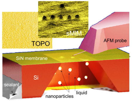
The need in imaging and spectroscopy of nano- and mesoscopic objects immersed in a liquid or gaseous environment resulted in remarkable progress in development of variety of optical, scanning probe, electron and x-ray microscopies during the last two decades and is currently used in biomedical, environmental and materials research. The new methods include scanning near-field optical microscopy,1 an array of novel far field super-resolution optical techniques,2 scanning electrochemical microscopy,3 high speed and resolution in-liquid atomic force microscopy (AFM),4 transmission and scanning electron microscopies (TEM and SEM) in liquids5, 6 as well as atmospheric-pressure in situ x-ray microscopy and spectroscopy.7
In spite of this great selection of the imaging modalities, specific applications often cannot be addressed with available instrumentation. As an example, near-field and super-resolution optical imaging rely on fluorescent dyes, which may be photobleached or altered by a highly acidic or alkaline chemical environment of an electrochemical experiment. Another challenge occurs when highly toxic, corrosive, or radioactive samples are to be studied in situ. For instance, chemical protection of the probe in a scanning electrochemical microscope does not isolate the rest of the instrument from corrosive vapors during in situ measurements in many liquid electrolytes. Alternatively, oxygen, nitrogen, and moisture of ambient environment can interfere with highly reactive samples. Placement of a probing tool inside a glove box is often not a viable option. In many cases, an attractive and universal solution is to enclose a sample in a molecularly impermeable and chemically inert enclosure. This approach has been successfully demonstrated in recent in situ TEM, SEM, and x-ray microscopy studies8 enabled by microfabricated closed or fluidic environmental cells with ultrathin electron- and x-ray-transparent membranes.9–11 However, local radiation damage and radiolysis induced by high-energy electron or x-ray beams during high-resolution imaging of hydrated objects often lead to deterioration of biological objects or adversely affect nanoscale chemical processes.12 A less invasive microscopy techniques based on low-energy penetrating radiation is highly desired.
Here, we propose and test a general concept of in situ imaging of reactive and biological samples based on near-field microwave microscopy in environmental cells, where samples are separated from ambient by ultra-thin membranes transparent for microwave radiation. Microwave imaging at a macro-scale is a mature technology with applications spanning from mapping the cosmic microwave background13 to seeing-through-the-wall and tomographic techniques.14, 15 The energy of microwave photons is a few tens of microelectronvolts. Under such low-energy excitation, neither electronic structure, nor chemical bonds in condensed matter are affected, and therefore, parasitic effects such as radiolysis, radiation damage, photobleaching, etc., common to the electron, x-ray, and optical microscopy, can be completely eliminated. At the nanoscale, the ability of near-field microwave microscopy to image buried and optically opaque structures has been realized shortly after invention of the technique and was experimentally demonstrated in imaging of three-dimensionally inhomogeneous solid structures, mainly related to semiconductor technology.16–19 Different from prior examples of microwave imaging in liquids,20, 21 our approach allows for full isolation of a sample from ambient as well as from the rest of the microscope and yet largely benefits from the resolution and analytical capabilities of the modern scanning probe microscopy.
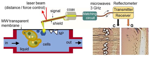
In our experiments, we use near-field microwave imaging known as Scanning Microwave Impedance Microscopy (sMIM). The principle of sMIM in liquids is depicted in the Figure 1. sMIM exploits the quasi-static electromagnetic fields formed at the apex of a sharp scanning probe connected to an end of a microwave transmission line, as schematically shown in Figure 1. The sharp probe concentrates microwave electric field between the tip and the sample.22 Variations of local permittivity and conductivity of the material under the probe during scanning lead to alterations of the capacitance and high-frequency conduction of the probe-sample system, which are monitored by a detection scheme based on a microwave reflectometer (Figure 1). The quasi-static electric component of the near field at the probe apex penetrates into a sample beneath the tip-sample contact, and thus, the tip-sample capacitive coupling ensures the subsurface sensitivity of the technique. The reflectometer circuit is designed to monitor changes of the real and imaginary parts of the admittance of the probe-sample system in two separate channels C and G (Figure 1), corresponding to variations the capacitance and conduction and resembling in this respect the output information of a conventional inductance-capacitance-resistance (LCR) meter. For sMIM, we place objects in a liquid solution into a sealed capsule or cavity, while leaving the probe outside the cavity. One of the walls of the capsule is made of a 8 nm to 50 nm thick SiN or SiO2 membrane, which has a sufficient mechanical strength to sustain the pressure difference between ambient and the capsule interior as well as an additional pressure imposed by the probe tip in contact with the membrane. The estimated probing depth inside the cavity is a few tip-membrane contact radii, i. e., a few hundreds of nm or less, and therefore, the processes and objects in the proximity of the membrane can be characterized. The spatial resolution of microwave imaging depends on the probe size and membrane thickness. In the experiments, we find that it exceeds the diffraction-limited resolution of optical microscopy for similar samples and is comparable to that of in situ liquid-cell SEM.
Figure 1.
Layout of the experimental setup for near-field scanning microwave impedance microscopy in liquids. An AFM-type scanning probe is integrated into an AFM setup for probe scanning over the sample surface with control of the probe-sample distance and force. In addition to the sample topography, two more channels—capacitance C and conductance G—are used for mapping and imaging. The capacitance and conductance of the tip-sample system are monitored by a microwave reflectometer operating at a frequency of 3 GHz. The objects under study are enclosed in a capsule filled with a fluid (or gas) and separated from the probe by an ultrathin dielectric membrane transparent for microwave radiation.
Results and Discussion
Modeling sensitivity, probing depth, and spatial resolution
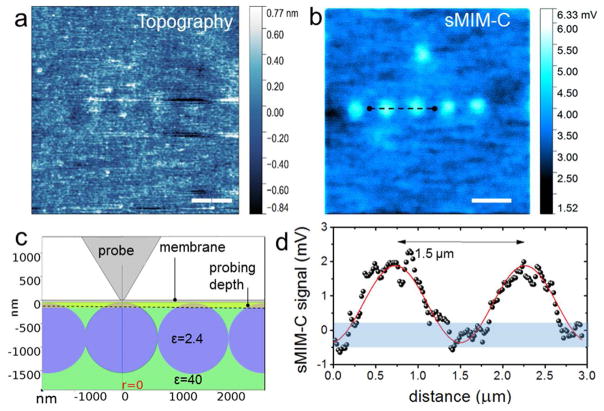
To test the feasibility of the near-field microwave imaging through membranes, we first imaged a well-defined model system consisting of a chain of 1.5 μm diameter polystyrene nanoparticles in glycerol beneath a 50 nm thick SiN membrane. To prepare the test samples, the colloid water solution of polystyrene particles was drop-cast into a cavity of a commercial SiN membrane chip of the style used for sample support in TEM studies. After drying, the particles adhered to the membrane surface and the cavity was filled with glycerol and sealed. Figures 2a and b show simultaneously acquired typical height (topography) and sMIM-C images, respectively. Polystyrene particles are not seen in the height image of the membrane, while an array of particles is well-resolved in the sMIM-C image in Figure 2b demonstrating the sMIM capability to probe the media through the tens of nanometers-thick membrane. The particles (relative dielectric permittivity ε = 2.4) appear brighter in the sMIM-C image relative to glycerol due to a higher dielectric constant of glycerol (ε = 40). The absence of the characteristic streaks in the height image in Figure 2a indicates a high mechanical stability of the membrane under the contact with the probe during scanning in the contact mode. The nearly perfect linear array made up by the five particles in the image, with particles equidistantly located in-line with a separation equal to the particle diameter of 1.5 μm, indicates that the particles are in contact with each other. This closely packed linear chain occurred due to evaporation-induced particle self-organization prior to filling the cell with glycerol. The in-line arrangement of the particles allows estimation of the probing depth of the microscope assuming a spherical shape of the particles as illustrated in Figure 2c. Figure 2d shows a line profile of probe-sample capacitance change across a pair of particles. Since the apparent diameter of the particles defined from the sMIM-C profile is about one-half of the particle diameter, we concluded that the probing depth below the 50 nm thick membrane is ca. 100 nm for this particular system.
Figure 2. Microwave imaging of a test sample.
a, Height and b, sMIM-C images of polystyrene particles in glycerol closely packed on the backside of a 50 nm-thick SiN membrane. c, Schematic illustrating the determination of the probing depth of the microscope. d, Experimental line profile (circles) and an eye guiding line (red) across the two bright spots in the sMIM-C image in b. The values of the capacitance change were obtained after calibration of the microscope sensitivity, 1.6 aF/mV in this experiment. The shadowed band corresponds to the signal noise level of 0.7 mV defined as root mean square deviation of the output voltage noise multiplied by the calibration factor). Scale bars in a and b are 4 μm.
To define the capabilities and fundamental limitations of sMIM for in situ imaging of enclosed nanoscale objects, we have performed numerical simulations of the tip-sample capacitance using model systems. The sMIM signal and image contrast depend on the sample permittivity, size of the objects, dielectric properties of the liquid media, probing depth, and parameters of the sample capsule layout, such as membrane thickness and permittivity.
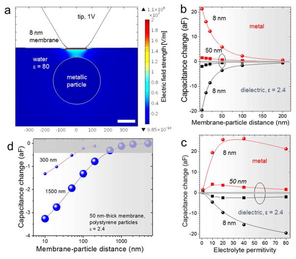
For simulations, we used 2D-axisymmetric models with spherical particles immersed in liquids under dielectric (ε = 9) membranes. The modeling was performed for dielectric (ε = 2.4) and metallic particles in liquids of variable dielectric permittivity and located coaxially with the probe tip. Two membrane thicknesses of 8 nm and 50 nm were considered. Figure 3a exemplifies a calculated map of electric field strength in proximity of a metallic particle with a diameter of 300 nm immersed in water (ε = 80) at a distance of 50 nm from a 8 nm-thick dielectric membrane. The tip-membrane contact radius in the model was set to 50 nm. The map highlights the strength of the electrical coupling between the probe tip apex and the particle through the membrane and water layer.
Figure 3.
(a) A map of the electric field strength E in the vicinity of the probe tip apex over a spherical metallic particle of a 300 nm diameter (highlighted by the white circle) immersed in water under a 8 nm-thick membrane with a relative dielectric permittivity ε = 9. The membrane-particle distance is 50 nm. The probe potential was set to 1 V. (b,c) Plots of the change of the probe-sample system capacitance upon introduction of a particle in a uniform liquid under the probe tip, similar to the configuration depicted in (a). (b) Capacitance change as a function of the membrane-particle distance for particles immersed in water (ε = 80). Probe-sample contact radius was 50 nm in the models used to obtain the plots. (c) Capacitance change as a function of the liquid permittivity for a metallic particle and a dielectric particle with a permittivity of 2.4. The particles are of 300 nm diameter and are in contact with the membrane. The plots are displayed for membrane thicknesses of 8 nm and 50 nm. (d) Curves of calculated capacitance vs. membrane-particle distance for 300 nm and 1.5 μm-diameter polystyrene particles (ε = 2.4) in water. The tip-membrane contact radii in the models were 50 nm and 20 nm, respectively; membrane thickness was 50 nm with ε = 9. The gray bar in (b–d) corresponds to the lowest achieved signal noise level in the sMIM-C measurements (0.4 aF), defined as root mean square deviation of the output voltage noise multiplied by the calibration factor.
To illustrate the influence on the membrane thickness on the signal strength, Figure 3b displays change in the capacitance of the probe-sample system relative to uniform liquid background as a function of liquid permittivity. The same quantity is plotted in Figure 3c as a function of the membrane-particle distance. As can be expected, a thinner membrane provides a stronger capacitive coupling and, consequently, a larger microscope signal in response to variation of the sample properties. The simulated capacitance change is about 5 times larger for a 8 nm thick membrane as compared to a 50 nm thick membrane. Therefore, the image contrast is expected to be strongly enhanced for ultrathin membranes with a thickness below 10 nm and, oppositely, becomes negligible if the membrane thickness exceeds 100 nm.
We performed similar modeling for spherical polystyrene particles of a 1.5 μm diameter in glycerol under a 50 nm SiN membrane. The simulation results were compared with the experimental data of Figure 2d. Note that the measured full signal change over the line profile in Figure 2d is 4.0 aF. The corresponding numerical model yielded a capacitance change of 4.1 aF, if the probe-sample contact radius is set to 20 nm. The latter value can be used as an estimate of the tip-membrane contact size in the experiments and was used in further simulations with the 1.5 μm particles. The simulations showed that the particle size has a strong effect on the microscope response. Figure 3d displays the calculated capacitance vs. membrane-particle distance for the 300 nm and 1.5 μm diameter particles and a 50 nm thick membrane (ε = 9). The tip-membrane contact radii in the models were 50 nm and 20 nm, respectively. As seen, despite a larger tip-membrane contact radius in the model with the 300 nm particle, the maximal depth, where the particle can be detected, is noticeably smaller than with the 1.5 μm one. This is an important result strongly pointing to a significant contribution of the side surfaces of the probe tip in the capacitance change in the case of larger objects. This effect is adverse for the high-resolution imaging; however, it can be reduced with use of thinner membranes. On the other hand, further simulations revealed a strong effect of the tip-membrane contact radius on the signal strength and depth sensitivity. This property of the probe can be employed for tomographic imaging with varying tip apex and tip-membrane contact size, similar to tomography with antennas of a varying aperture proposed by Gaikovich.14
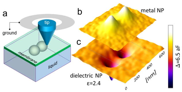
We further carried out simulations of the capacitance images from metallic and dielectric particles to estimate the spatial resolution of imaging through membranes. As sketched in Figure 4a, the model sample consisted of two identical 300 nm nm-diameter particles in contact to each other and with a 8 nm-thick membrane (ε = 9). The particles are immersed in water (ε = 80). The simulated capacitance maps are presented in Figures 4b and c as 3D surfaces of capacitance difference over water background for pairs of dielectric (ε = 2.4) and metallic particles, respectively. As seen, the particles are well resolved in the maps. From the capacitance map in Figure 4c, the maximal capacitance change relative to the pure water background for a pair of metallic particles is 3.3 aF. The lowest achieved noise floor of the sMIM system used in our experiments (defined as root mean square deviation of the output voltage noise multiplied by the calibration factor) was about 0.4 aF. Taking into consideration that the capacitance C of a metal particle of a diameter D scales as C ~ D2, one can conclude that ca. 100 nm-diameter nanoparticles can be resolved through a 8 nm thick membrane with the current sMIM electronics. However, the spatial resolution can be increased using thinner membranes and through sensitivity enhancement of the measurements system. The spatial resolution in the sMIM experiments can be treated in the same theoretical framework as one developed for other near-field-based scanning probe microscopies, e. g., Kelvin probe microscopy, magnetic force microscopy, or piezoresponse force microscopy.23 Overall, the spatial resolution of sMIM imaging depends on the probe tip apex radius, membrane thickness, contrast of the material properties, and microscope sensitivity relative to the measurements noise. A practical compromise between a number of parameters has to be found in experiments for any particular system under study to optimize imaging. With optimized conditions, a resolution of ca. 50 nm can be achieved for metallic objects with the commercially available probes with ca. 50 nm tip apex radius. Such resolution is comparable to that demonstrated by SEM in liquids.24
Figure 4.
(a) Schematic layout of the 3D model used to calculate capacitance maps shown in (b) and (c). Diameter of the spherical particles is 300 nm, membrane thickness is 8 nm, and permittivity is 9. The particles are immersed in water and are in contact with the membrane. Simulated probe-sample capacitance maps over pairs of (b) dielectric and (c) metallic particles. Permittivity of the dielectric particle material is 2.4. The full range of the color scale for capacitance is 6.5 aF. Probe-membrane contact radius was 20 nm in the models.
Imaging of an electrochemical process
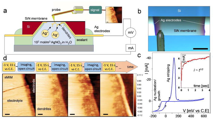
We follow with a set of experiments demonstrating in situ microwave imaging of the dendrite growth near electrodes in a water solution. We note first that the electromagnetic field in a media under the probe tip cannot drive any chemical transformations in the electrolyte (see Methods sections for details). For the experiments, two thin-film silver electrodes with a thickness of about 50 nm were deposited on the backside of 50 nm thick SiN membranes and supporting Si chip through a conformal shadow mask. The cross-section of the cell layout with the SiN membrane, electrodes, and Si frame is shown in Figure 5a. After that, the cavity in the Si chip was filled with ca. 10 μL of a 102 mol/m3 AgNO3 solution in water and sealed (Figure 5a). The sMIM imaging was performed from the membrane side of the cavity as shown in Figures 5a and b.
Figure 5.
(a) Layout of the electrochemical environmental cell for sMIM imaging in liquid electrolytes. Its major difference from the cell depicted in Figure 1a is the presence of the electrodes on the backside of the dielectric membrane. (b) Optical image of top of the cell with an sMIM probe over the SiN membrane. (c) A cyclic voltammogram of Ag growth and stripping at/from a Ag electrode of the environmental cell. Inset: the anodic current as a function of time after a bias of −200 mV was applied to the electrode vs. a quasi Ag reference electrode. (d) A sequence of the applied potential (−1 V, 15 s) steps followed with sMIM-C maps of electrochemical Ag dendritic growth on Ag cathode taken at open circuit condition. Scale bar in (b) is 100 μm. Scale bars in (d) are 2 μm.
Prior to sMIM imaging, the process of Ag electroplating was tested quantitatively using a separate replica cell. A cyclic voltammogram (CV) of Ag electrodeposition at a 50 nm thick Ag electrode in Figure 5c shows a characteristic hysteresis appearing after the reversal of the potential sweep followed by a sharp anodic peak of Ag stripping. The presence of the reverse cathodic wave is consistent with dendrite-type geometry of the growing deposit, whose surface area continues to increase with time after the change in the potential sweep direction. No such feature would be observed for two-dimensional (layer-by-layer) electrodeposition. When a potential of −200 mV vs. Ag quasi-reference electrode is applied, the deposition transient showed an initial spike of charging current as a function of time (inset in Figure 5c) followed by characteristic current increase proportionally to the square root of time, as expected based on the results of ref 25. During subsequent sMIM imaging, a somewhat larger overpotential of −1 V was applied to facilitate observable silver deposition within a fraction of a minute.
Figure 5d displays a sequence of sMIM images obtained by applying −1.0 V to one of the Ag electrodes for 15 s at each step. The circle was kept open during few minutes sMIM scan. The leftmost panel shows the initial state of Ag cathode edge (dark area on the right) immersed into solution (light area on the left). The stripe of about 2 μm width along the electrode edge is a thinner part of silver film formed due to metal deposition through the shadow mask during electrode fabrication. After the first 15 s of chronoamperometry at −1.0 V, one can clearly resolve the metallic dendrites growing from the electrode edge along the entire length of the electrode. Second application of the voltage for another 15 s leads to further dendrite growth. The dendrites length increases, accompanied by coarsening and thickening of the dendrite structure. However, the third application of the voltage (followed by opening the circuit) did not lead to appreciable new dendrite growth. This is presumably due to loss of electrical connection between dendrites and the electrode as a result of dissolution of the thinnest Ag film portion at the electrode edge, seen as the white stripe in the rightmost panel of Figure 5c. Such a behavior can be explained by deposition/dissolution kinetics with the rate constant for the Ag dissolution and deposition reactions approaching characteristic time for Ag+ mass transport. Namely, Ag ions become depleted near the electrode during the deposition, and therefore, under the open circuit condition, a part of the electrode and of the deposit can be dissolved back into solution to compensate for the depletion.26 The process will take place until the annihilation of the Ag+ gradient by diffusion of Ag+ from solution and from the electrode.
Comparison of microwave and SEM images
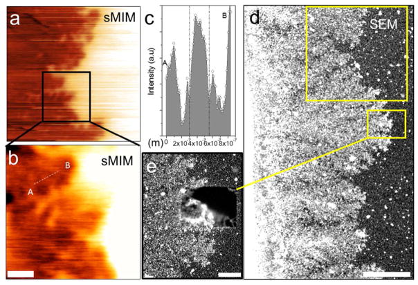
Next, we perform side-by-side comparison of sMIM and SEM images using the same set of samples. Figures 6a and b display a 12 μm × 12 μm sMIM image of the dendrite tips and a close-up, 5 μm × 5 μm, image of a portion of the same structure. The contrast in the close-up image was enhanced to highlight smaller details and inhomogeneities in the structure, which cannot be seen in the larger-scale image in Figure 6a. The image reveals a granular-like, three-dimensional morphology of the dendrites. The spatial resolution can be estimated from the line profile across a small, clearly resolved wedge-like feature in the Figure 6b image. The full width at half maximum (FWHM) of the signal peak through a gap between two metallic branches of a dendrite yields approximately 250 nm. This exceeds the resolution of the standard optical microscopy for these samples by a factor of two. However, we notice that the metallic branches are still visually discernible is a distance about half of this, that is close to the 100 nm predicted by the numerical simulations discussed above.
Figure 6.
(a) 12 μm × 12 μm and (b) 5 μm × 5 μm sMIM-C in situ images of the Ag dendrites electrochemically grown at a Ag electrode in a 102 mol/m3 AgNO3 water solution. The images were obtained through a 50 nm SiN membrane. The signal value along the line AB have been selected for resolution evaluation. (c) Full width at half maximum of the signal peak along the line cut AB through two metallic branches of a dendrite in (c) is approximately 250 nm. (d) The same area as in (a) imaged using SEM. Scale bar corresponds to 5 μm. The electron beam energy was set to 15 keV. (e) Electron-beam-induced dissolution/delamination of Ag deposit from the backside of the membrane. Scale bar corresponds to 1 μm.
After sMIM experiments, the same area was inspected using a liquid SEM. Figure 6c shows a low resolution SEM image of the same dendritic area as in Figures 6a and b. Bright contrast of the dendrites corroborates with their higher density and larger Z number compared to the surrounding liquid. In addition to the dendritic deposit at electrode, the contrast enhancement of SEM image in Figure 6c reveals the presence of small bright nanoparticles over the entire SEM field of view. The latter deposit is presumably due to electron beam induced Ag precipitation from the solution as a result of a Ag reduction reaction Ag+ + e− = Ag0, where e− is a solvated electron. Given the complexity of the electron-beam-induced chemistry in water,12 a number of alternative reactions may occur leading to precipitation of AgOH, AgO and Ag2O.27 The attempt to acquire high-resolution image with a field-of-view comparable to that in Figure 6b resulted in adverse effects of aggregation, delamination and dissolution of Ag dendrites (Figure 6d). This complex behavior of ionic solutions under electron beam irradiation has been reported previously28 and was explained by a dose-dependent partitioning of reducing and oxidizing species generated in water during the beam-induced radiolysis.12 High-magnification SEM imaging unavoidably leads to significant radiolysis in liquids, which complicates the study of interfaces in ionic solutions. The sMIM imaging, on the other hand, is nondestructive, free from such artifacts and can be readily applied to electrochemical studies.
Identification of dielectric and metallic reaction products
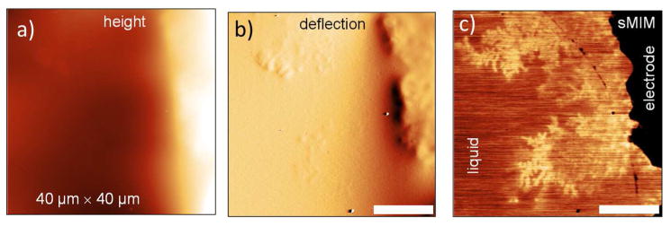
Further experiments revealed another advantage of microwave imaging over the electron microscopy. In contrast to electron microscopy, which is predominately sensitive to the material density, the microwave imaging is capable of unambiguous discrimination between dielectric and metallic objects. To illustrate this, Figures 7a–c show a dendrite structure grown after few seconds short high negative (−3 V) potential applied to silver electrodes. The microwave image in Figure 7c, recorded at open circuit conditions, reveals contrast inversion between dendrites and water solution in comparison with the metallic dendrites of the previous experiment, indicating that dendrites are dielectric formed of oxidized Ag deposit. Growth of similar deposits was previously shown to occur due to intensive water splitting near the electrode accompanied by diffusion-limited oxidation and precipitation of Ag ions directly from the solution as well as fast oxidation of already grown Ag dendrites.27, 29
Figure 7.
(a–c) Topography, deflection error, and sMIM-C images, respectively, of dendrites formed after a −3 V overpotential was applied shortly to the Ag electrode and circuit was left open during image acquisition. Scale bars are 10 μm.
Imaging of live biological cells
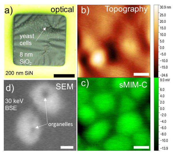
Next, we evaluate the applicability of the sMIM for in situ imaging of live biological objects in liquids. Water- and glycerol-based solutions were selected for these experiments due to their importance in biological studies, for example for cryoprotection of specimens.30 The imaging experiments were carried out with saccharomyces cerevisiae yeasts cells. Prior to the imaging, the cells from a budding solution were dispersed in water or glycerol and drop-casted onto the backside of a membrane chip with 8 nm-thick SiO2 membranes. After that, the cavity in the membrane chip was sealed. Figure 8a demonstrates a typical optical image of yeast cells immersed in a ca. 50 % mol/mol glycerol solution in water taken through the 8 nm thick SiO2 membrane in reflection mode. The high viscosity of glycerol helps to suppress Brownian motion and promotes adhesion of the cells to the membrane; thus, the cells are immobilized and can be easily imaged in the scanning probe experiments. Figure 8b shows the topographic image of the 8 nm thick SiO2 membrane. The image reveals membrane corrugation, which is due to membrane bending under the probe and mechanical interaction of the membrane with the yeast cells underneath. At the same time, the image demonstrates a sufficient rigidity of the 8 nm-thick membrane for scanning in the contact mode. More details can be seen in the simultaneously acquired sMIM-C image in Figure 8c, where a larger number of yeast cells is visible as bright areas against the background of glycerol solution. The contrast indicates a lower dielectric constant of the yeast cells compared to that of glycerol. A fraction of the cells seen in the sMIM-C image also appeared in the topography image, which shows that the cells in the microwave image are in contact with the backside of the membrane.
Figure 8.
(a) A wide-field optical microscopy image of yeast cells immersed in glycerol behind a 8 nm-thick SiO2 membrane. (b) sMIM topography channel shows that cell’s adhesion to SiO2 membrane affects the morphology of the membrane. (c) sMIM-C image of the same area as in (b). A larger number of visible cells is due to the probing depth of microwaves. (d) Scanning electron microscopy image of the yeast cells immersed in water solution. See details in the text. Scale bar in a is 20 μm. Scale bars in (b–d) are 1 μm.
For comparison, SEM imaging of the similar samples have been performed using backscattered electron detector (BSE). Importantly, SEM imaging of the yeast cells in glycerol was not possible due to severe beam-induced effects caused by the reduced recombination kinetics of radiolysis products in glycerol.31 However, the cells were successfully imaged in pure water for the comparison of the capabilities of the two imaging techniques. In the SEM image obtained with BSE detector and shown in Figure 8d, the cells appear brighter compared to the background water indicating their higher average Z number and/or a higher density of cellular walls. The dark areas visible within the cells are presumably organelles, which have a smaller density compared to the cellular liquid and the cell membrane walls.24,32 This is in contrast with the sMIM images, where no intracellular structure could be resolved. To interpret this result, we note that the probing depth of SEM is in the micrometer range at the electron beam energy of 30 eV used to obtain the image in Figure 8d, while the probing depth of the sMIM of a few hundreds of nanometers is about one order of magnitude smaller. Thus, the contrast in the sMIM-C image is determined by the low dielectric permittivity of the lipid membranes (ε ≈ 3 33) of the yeast cells, while the intracellular liquid mainly contributes to the contrast in the SEM image. We note that the spatial resolutions of the two techniques are comparable in these experiments. However, similar to the imaging the electrochemical processes described above, sMIM has an advantage of being noninvasive, while severe radiolysis and radiation damage of biological tissues are commonly observed during liquid SEM.
Conclusions
We have introduced and demonstrated a scanning probe technique for in situ imaging in liquid and gaseous environments with probes and samples separated by ultrathin membranes. For imaging, objects under study are placed into a sealed capsule or cavity filled with a fluid. To ensure probe-sample coupling and subsurface detection under membranes, penetrative properties of microwave near-fields concentrated by the sharp scanning probe are used. The major advantage of microwaves as a penetrating probe for imaging is its noninvasive nature since electronic excitation of the media or the sample does not occur, and negligible energy transferred to the sample in the form of heat quickly dissipates into the liquid. The latter makes this imaging technique ideally suited to artifact free exploration of surfaces and subsurface regions of live biological samples and interfacial (electro-) chemical processes. We applied the microwave imaging through membranes to probe dendrite growth in Ag electroplating and live yeast cells in situ in liquids, and compared the microwave images with the images of the same samples obtained with SEM. We showed that the microwave imaging is free from radiolysis and radiation-induced damage inherent in SEM and in other imaging techniques exploiting high-energy particles or radiation. Depending on the tip-membrane contact radius and membrane thickness the resolution and the probing depth of this technique can be in the range of tens and hundreds of nanometers, respectively, that makes it comparable to modern super-resolution optical imaging and scanning electron microscopy in liquids. Extensive numerical modeling supported the experimental results. The thinnest, 8 nm thick, SiO2 membrane used in the experiments showed a high mechanical stability in the contact mode imaging. It can be concluded that the membrane thickness can be further reduced to increase the spatial resolution and the sensitivity, potentially with graphene or h-BN used as membrane materials. In addition, the approach can serve as a framework for in situ nanoscale tomography with varying tip-apex size to achieve a varying depth sensitivity. Furthermore, our approach, where samples are incased inside a molecularly impermeable and chemically inert enclosure, can be especially useful for studies of highly reactive, toxic or radioactive media as well as materials available in minuscule amounts, e.g. in forensics. Finally, the technique can be easily coupled with microfluidic platforms what will allow facile sampling of different liquids and gases as well as implementation of electrical, electrophoretic, osmotic, etc. sample controls.
Methods
Microwave imaging and modeling
Microwave imaging was performed using a commercial near-field microwave AFM platform using fully shielded probes. The probes with a nominal spring constant of 7 N/m to 9 N/m were provided by the manufacturers of the imaging system and are fully compatible with the standard laser-beam-based probe-sample force control of the AFM. The sensing tip of the probes is made of a Ti/W alloy with a nominal tip apex radius of 50 nm as specified by the manufacturer. The tip-sample contact size can be adjusted by controlling the tip-sample contact force. The microwave power during imaging was set to 40 μW (−14 dBm). The microscope sensitivity was calibrated using a commercial calibration kit for microwave microscopy. Numerical simulations were performed with a commercial finite-elements modeling software package.
The ac voltage amplitude at the probe tip can be estimated based on the power of the microwave source. For the power of 40 μW used in the imaging experiments, the voltage amplitude at the probe tip does not exceed 127 mV. This is an overestimation since this value can be reached only neglecting losses along the transmission line and microwave circuits along it. The duration of the half-cycle of the microwave voltage at the 3 GHz frequency is about 170 ps. Besides the fact that these voltage is too low to activate parasitic chemical processes such as water splitting reaction, the half-cycle time is too short for significant kinetic processes related with ions diffusion in liquid, to occur. For example, an electric field of 107 V/m, which may be present under the probe tip at a dc bias , would (oscillatory) move monovalent ions with a typical mobility of 10−7 m2/(s · V) by only ca. 0.1 nm during 100 ps.
Environmental cell design and fabrication
Commercial SiN 50 nm thick and SiO2 8 nm thick membranes on Si frames were used. Two 50 nm thick Ag electrodes were evaporated onto cavity side of the Si frames using a PDMS mold as a conformal shadow mask. Two flexible planar leads were glued to the thin-film silver electrodes using a silver epoxy. The leads and most of the Ag electrode area were encapsulated using an UV curable epoxy (as shown in Figure 6a). The cavity with the membrane window and electrodes was filled with a liquid sample. A microporous filter was placed on top of the cavity with the liquid sample, and after that, the entire assembly was sealed using a UV curable epoxy.
Sample fabrication
Dry active saccharomyces cerevisiae yeasts cells (2 g) were thoroughly mixed in warm (from 28 °C to 33 °C) 3 · 102 mol/m3 sucrose solution in type I water. The mixture was left at the same temperature under aerobic environment for few hours before experiments. For imaging, ca. 5 μL of solution was dispersed in the same amount of type I water or glycerol, drop-casted on to the backside of a 8 nm thick SiO2 membrane, and sealed. The imaging took place within 20 min. after sealing the environmental cell. For Ag electroplating, ca. 10 μL of a 102 mol/m3 AgNO3 solution in water was drop-casted on a 50 nm thick SiN membrane window with Ag electrodes; after that, the cell was sealed.
SEM imaging
SEM imaging was performed following the microwave imaging of the same samples. Depending on the membrane thickness, liquid media and imaged objects, an Everhart-Thornley type or BSE electron detector was used. The energy of the primary electron beam varied between 2 keV and 30 keV.
Acknowledgments
Microwave imaging was conducted at the Center for Nanoscale Science and Technology, NIST and at the Center for Nanophase Materials Sciences, ORNL, which also provided support (A.T., A.I., S.V.K) and which is sponsored at Oak Ridge National Laboratory by the Scientific User Facilities Division, Office of Basic Energy Sciences, U. S. Department of Energy. A.T. acknowledges support by U.S. Civilian Research and Development Foundation. J.V. work was supported via NIST-CNST/UMD-IREAP Cooperative Agreement. Authors are thankful to Dr. K. Siebein for the experimental support and to Dr. T. Moffat, Dr. M. Stiles and Dr. N. Zhitenev (all at NIST) for their valuable discussions.
Footnotes
Notes
The authors declare no competing financial interests.
References
- 1.Betzig E, Trautman JK. Near-Field Optics: Microscopy, Spectroscopy, and Surface Modification Beyond the Diffraction Limit. Science. 1992;257:189–195. doi: 10.1126/science.257.5067.189. [DOI] [PubMed] [Google Scholar]
- 2.Chen BC, Legant WR, Wang K, Shao L, Milkie DE, Davidson MW, Janetopoulos C, Wu XS, Hammer JA, Liu Z. Lattice Light-Sheet Microscopy: Imaging Molecules to Embryos at High Spatiotemporal Resolution. Science. 2014;346:1257998. doi: 10.1126/science.1257998. [DOI] [PMC free article] [PubMed] [Google Scholar]
- 3.Amemiya S, Bard AJ, Fan FRF, Mirkin MV, Unwin PR. Scanning Electrochemical Microscopy. Annu Rev Anal Chem. 2008;1:95–131. doi: 10.1146/annurev.anchem.1.031207.112938. [DOI] [PubMed] [Google Scholar]
- 4.Ando T, Uchihashi T, Kodera N, Yamamoto D, Miyagi A, Taniguchi M, Yamashita H. High-Speed AFM and Nano-Visualization of Biomolecular Processes. Pflug Arch Eur J Phy. 2008;456:211–225. doi: 10.1007/s00424-007-0406-0. [DOI] [PubMed] [Google Scholar]
- 5.de Jonge N, Ross FM. Electron Microscopy of Specimens in Liquid. Nat Nanotechnol. 2011;6:695–704. doi: 10.1038/nnano.2011.161. [DOI] [PubMed] [Google Scholar]
- 6.Thiberge S, Nechushtan A, Sprinzak D, Gileadi O, Behar V, Zik O, Chowers Y, Michaeli S, Schlessinger J, Moses E. Scanning Electron Microscopy of Cells and Tissues under Fully Hydrated Conditions. P Natl Acad Sci USA. 2004;101:3346–3351. doi: 10.1073/pnas.0400088101. [DOI] [PMC free article] [PubMed] [Google Scholar]
- 7.Bluhm H, Andersson K, Araki T, Benzerara K, Brown GE, Dynes JJ, Ghosal S, Gilles MK, Hansen HC, Hemminger J. Soft X-Ray Microscopy and Spectroscopy at the Molecular Environmental Science Beamline at the Advanced Light Source. J Electron Spectrosc. 2006;150:86–104. [Google Scholar]
- 8.Guay D, Stewart-Ornstein J, Zhang X, Hitchcock AP. In Situ Spatial and Time-Resolved Studies of Electrochemical Reactions by Scanning Transmission X-Ray Microscopy. Anal Chem. 2005;77:3479–3487. doi: 10.1021/ac048077j. [DOI] [PubMed] [Google Scholar]
- 9.Kolmakov A, Dikin DA, Cote LJ, Huang J, Abyaneh MK, Amati M, Gregoratti L, Günther S, Kiskinova M. Graphene Oxide Windows for in Situ Environmental Cell Photoelectron Spectroscopy. Nat Nanotechnol. 2011;6:651–657. doi: 10.1038/nnano.2011.130. [DOI] [PubMed] [Google Scholar]
- 10.Yuk JM, Park J, Ercius P, Kim K, Hellebusch DJ, Crommie MF, Lee JY, Zettl A, Alivisatos AP. High-Resolution Em of Colloidal Nanocrystal Growth Using Graphene Liquid Cells. Science. 2012;336:61–64. doi: 10.1126/science.1217654. [DOI] [PubMed] [Google Scholar]
- 11.Stoll JD, Kolmakov A. Electron Transparent Graphene Windows for Environmental Scanning Electron Microscopy in Liquids and Dense Gases. Nanotechnology. 2012;23:505704. doi: 10.1088/0957-4484/23/50/505704. [DOI] [PubMed] [Google Scholar]
- 12.Schneider NM, Norton MM, Mendel BJ, Grogan JM, Ross FM, Bau HH. Electron–Water Interactions and Implications for Liquid Cell Electron Microscopy. J Phys Chem C. 2014;118:22373–22382. [Google Scholar]
- 13.de Bernardis P, Ade PA, Bock J, Bond J, Borrill J, Boscaleri A, Coble K, Crill B, De Gasperis G, Farese P. A Flat Universe from High-Resolution Maps of the Cosmic Microwave Background Radiation. Nature. 2000;404:955–959. doi: 10.1038/35010035. [DOI] [PubMed] [Google Scholar]
- 14.Gaikovich KP. Subsurface Near-Field Scanning Tomography. Phys Rev Lett. 2007;98:183902. doi: 10.1103/PhysRevLett.98.183902. [DOI] [PubMed] [Google Scholar]
- 15.Semenov SY, Svenson RH, Bulyshev AE, Souvorov AE, Nazarov AG, Sizov YE, Posukh VG, Pavlovsky A, Repin PN, Starostin AN, et al. Three-Dimensional Microwave Tomography: Initial Experimental Imaging of Animals. IEEE Trans Biomed Eng. 2002;49:55–63. doi: 10.1109/10.972840. [DOI] [PubMed] [Google Scholar]
- 16.Kopanski JJ, You L, Ahn JJ, Hitz E, Obeng YS. Scanning Probe Microscopes for Subsurface Imaging. ECS Trans. 2014;61:185–193. [Google Scholar]
- 17.Farina M, Di Donato A, Monti T, Pietrangelo T, Da Ros T, Turco A, Venanzoni G, Morini A. Tomographic Effects of near-Field Microwave Microscopy in the Investigation of Muscle Cells Interacting with Multi-Walled Carbon Nanotubes. Appl Phys Lett. 2012;101:203101. [Google Scholar]
- 18.Lai K, Ji MB, Leindecker N, Kelly MA, Shen ZX. Atomic-Force-Microscope-Compatible near-Field Scanning Microwave Microscope with Separated Excitation and Sensing Probes. Rev Sci Instrum. 2007;78:063702. doi: 10.1063/1.2746768. [DOI] [PubMed] [Google Scholar]
- 19.Plassard C, Bourillot E, Rossignol J, Lacroute Y, Lepleux E, Pacheco L, Lesniewska E. Detection of Defects Buried in Metallic Samples by Scanning Microwave Microscopy. Phys Rev B. 2011;83:121409. [Google Scholar]
- 20.Kim S, Yoo H, Lee K, Friedman B, Gaspar MA, Levicky R. Distance Control for a near-Field Scanning Microwave Microscope in Liquid Using a Quartz Tuning Fork. Appl Phys Lett. 2005;86:153506. [Google Scholar]
- 21.Farina M, Mencarelli D, Venanzoni G, Morini A. High Resolution Scanning Microwave Microscopy for Applications in Liquid Environment. IEEE Microw Wirel Compon Lett. 2012;22:595–597. [Google Scholar]
- 22.Anlage SM, Talanov VV, Schwartz AR. Principles of Near-Field Microwave Microscopy. In: Kalinin SV, Gruverman A, editors. Scanning Probe Microscopy: Electrical and Electromechanical Phenomena at the Nanoscale. Springer Scientific; New York: 2007. pp. 215–253. [Google Scholar]
- 23.Kalinin SV, Jesse S, Rodriguez BJ, Shin J, Baddorf AP, Lee HN, Borisevich A, Pennycook SJ. Spatial Resolution, Information Limit, and Contrast Transfer in Piezoresponse Force Microscopy. Nanotechnology. 2006;17:3400. doi: 10.1088/0957-4484/17/14/010. [DOI] [PubMed] [Google Scholar]
- 24.Thiberge S, Zik O, Moses E. An Apparatus for Imaging Liquids, Cells, and Other Wet Samples in the Scanning Electron Microscopy. Rev Sci Instrum. 2004;75:2280–2289. [Google Scholar]
- 25.Hills G, Schiffrin D, Thompson J. Electrochemical Nucleation from Molten Salts—I. Diffusion Controlled Electrodeposition of Silver from Alkali Molten Nitrates. Electrochimica Acta. 1974;19:657–670. [Google Scholar]
- 26.Andricacos P, Ross P. Diffusion-Controlled Multisweep Cyclic Voltammetry III. Deposition of Silver on Stationary and Rotating-Disk Electrodes. J Electrochem Soc. 1984;131:1531–1538. [Google Scholar]
- 27.Lützenkirchen-Hecht D, Strehblow HH. Anodic Silver (II) Oxides Investigated by Combined Electrochemistry, Ex Situ XPS and in Situ X-Ray Absorption Spectroscopy. Surf Interface Anal. 2009;41:820–829. [Google Scholar]
- 28.Noh KW, Liu Y, Sun L, Dillon SJ. Challenges Associated with in-Situ TEM in Environmental Systems: The Case of Silver in Aqueous Solutions. Ultramicroscopy. 2012;116:34–38. [Google Scholar]
- 29.Droog JMM, Huisman F. Electrochemical Formation and Reduction of Silver Oxides in Alkaline Media. J Electroanal Chem Interfacial Electrochem. 1980;115:211–224. [Google Scholar]
- 30.Hubalek Z. Protectants Used in the Cryopreservation of Microorganisms. Cryobiology. 2003;46:205–229. doi: 10.1016/s0011-2240(03)00046-4. [DOI] [PubMed] [Google Scholar]
- 31.Kajiwara T, Thomas J. Reactions of Electrons in Glycerol. The Journal of Physical Chemistry. 1972;76:1700–1706. [Google Scholar]
- 32.Bozzola JJ, Russell LD. Electron Microscopy: Principles and Techniques for Biologists. Jones & Bartlett Learning; 1999. [Google Scholar]
- 33.Gramse G, Dols-Perez A, Edwards MA, Fumagalli L, Gomila G. Nanoscale Measurement of the Dielectric Constant of Supported Lipid Bilayers in Aqueous Solutions with Electrostatic Force Microscopy. Biophys J. 2013;104:1257–1262. doi: 10.1016/j.bpj.2013.02.011. [DOI] [PMC free article] [PubMed] [Google Scholar]


