Abstract
This paper presents the design and preliminary evaluation of small-pixel CdTe gamma ray detectors equipped with a hybrid pixel-waveform (HPWF) readout system for gamma ray imaging applications with additional discussion on CZT due to its similarity. The HPWF readout system utilizes a pixelated anode readout circuitry which is designed to only provide the pixel address. This readout circuitry works in coincidence with a high-speed digitizer to sample the cathode waveform which provides the energy, timing, and depth-of-interaction (DOI) information. This work focuses on the developed and experimentally evaluated prototype HPWF-CdTe detectors with a custom CMOS pixel-ASIC to readout small anode pixels of 350 μm in size, and a discrete waveform sampling circuitry to digitize the signal waveform induced on the large cathode. The intrinsic timing, energy, and spatial resolution were experimentally evaluated in this paper in conjunction with methods for depth of interaction (DOI) partitioning of the CdTe crystal. While the experimental studies discussed in this paper are primarily for evaluating HPWF detectors for small animal PET imaging, these detectors could find their applications for ultrahigh-resolution SPECT and other imaging modalities.
I. Introduction
The years surrounding the turn into the twenty first century saw the engineering of some of the most prominent small animal imaging systems. A collection of works and the eventual success of systems from individuals such a S. R. Cherry and F. Beekman established the current state of the art which relies largely on scintillator based detectors for PET and SPECT applications [1-3]. The implementation of scintillators has proved greatly successful, but the necessity of pushing into the sub-millimeter range has triggered some recent explorations into alternative technologies, such as semiconductor detectors, such as silicon, CdTe and CdZnTe (CZT) [4-6].
While there has been substantial efforts for using finely pixelated scintillation detectors with 500 um wide crystal elements for achieving an ultrahigh PET imaging resolution by Cherry's group [7], physical difficulties still exist. Such challenges as finely segmenting the crystal elements, the inevitable loss in detection efficiency with size, finding photon detectors with sufficient spatial resolution and the resulting increase in cost begin to pose a challenge when a very high intrinsic spatial resolution is desired with compact geometries. This work analyzes the implementation of novel highly pixelated semiconductor detectors which offer excellent energy resolution, high intrinsic spatial resolution, adequate timing resolution, and simplified electronics.
CZT and CdTe based semiconductor detectors have been explored widely for medical imaging applications [8, 9]. The selection of these detectors yields a potential combination of excellent energy and spatial resolution combined with adequate detection efficiency for numerous single photon emitters. In recent years, several groups have evaluated the use of small pixel CZT/CdTe based imaging detectors as a potential replacement for scintillation detectors for high-resolution SPECT imaging applications [10-13]. Extensive effort towards building future PET based on CZT and CdTe detectors has been explored as well [14-20].
Efforts working in PET and SPECT have focused on implementing designs with the intention of replacing scintillation, these works, such as that of the MRC-SPECT-I, and the exploration of stacked crystal CdTe PET have exemplified the potential of the semiconductor material imaging modalities [14,21-23]. However, our detector work and system develop does not propose CdTe currently as a strict replacement for scintillation, but we rather focus on the development of technological approaches to utilize the key benefits of CZT and CdTe detectors, namely the potential of a ultrahigh intrinsic 3-D spatial resolution (sub-500 μm or even sub-250 μm), and an excellent energy resolution [24]. For those previous studies, it has been difficult to justify choice of CZT or CdTe over scintillation detectors, especially when considering the higher material cost, the need for more complex readout methods, the intrinsically lower detection efficiency per unit detector volume and the intrinsically poor timing properties associated with these semiconductor materials. These are elements we attempt to address and improve on in our current detector design.
We have recently proposed the hybrid pixel-waveform (HPWF) CZT/CdTe detector design that has the potential of offering an ultrahigh intrinsic spatial resolution in 3-D, an improved timing resolution and allows for a simplified readout system. While the HPWF detector technology may not replace scintillation detectors for general PET applications, it could be an attractive solution for building compact and ultrahigh resolution PET scanners for specific and high-impact applications, such as imaging beta amyloid (Aβ) plaques in mouse AD models [25, 26]. In this work, we have carried out a preliminary evaluation of prototype HPWF CdTe detectors placed in a dual-head coincidence setup. From this setup, we have experimentally verified the energy resolution, depth of interaction (DOI), and timing-resolution from the fitted cathode waveform and the shaped cathode waveform data. We further carried out a series of preliminary point source imaging studies to explore the potential attainable spatial resolution for PET using HPWF detectors. These studies analyzed the impact of DOI, inter-pixel scattering and positron range on the overall system resolution. These results are presented and discussed in this paper.
II. Challenges of Using Small Pixel CZT and CdTe Detectors for PET Imaging Applications
There are several challenges for using small-pixel CdTe and CZT detectors for ultra-high resolution PET imaging applications, especially when the size of anode-pixels is comparable or smaller to the average dimension of the secondary charge-cloud generated by the interaction of 511 keV gamma rays in CdTe and CZT materials.
First, it is well known that the use of small anode-pixels could lead to a degraded energy resolution. This is mainly due to the unrecoverable charge loss in the gap between anode pixels and the additional statistical fluctuations associated with the process of extracting the total induced signal from signals induced on adjacent pixels [27-29]. Various hardware workarounds have been implemented to improve the energy resolution. The first proposed solution involves placing steering electrodes between adjacent pixels in order to drive electrons more effectively toward the collecting electrodes [30, 31]. However, it becomes increasingly difficult to implement this approach for detectors with small pixel pitch (500 μm or below). Alternative methods have included multiple pixel readout followed by hardware summing as performed in Medipix detectors [32-34], or in post-acquisition software processing.
The second challenge for using CdTe/CZT detectors for PET application is limited timing resolution. CZT and CdTe material exhibit limited electron mobility μe of 1000-1100 cm2/Vs and 1000-1300 cm2/Vs [35, 37], respectively. This directly implies that the collection of electrons for thicker crystals could span the order of hundreds of ns. The long charge collection time, coupled to the finite signal-to-noise ratio from readout electronics, makes it difficult to achieve a timing resolution attainable with scintillation detectors (e.g. a few hundred ps [37-39]). Furthermore, the timing resolution could also be severely affected by the imperfections in CZT and CdTe materials and the electric field non-uniformity [40]. These limitations pose a greater challenge for using CZT/CdTe detectors for PET imaging.
The final challenge for using highly pixelated CZT/CdTe detectors for PET imaging is derived from the necessity to develop a readout system with a reduced complexity which can handle the numerous readout channels. The decrease in pixel size would imply a dramatically increased pixel density. Even with the rapid advance in readout electronics, an exploration into simplified circuitry is still warranted to minimize power consumption, reduce heat generation, improve cost-effectiveness, and maintain a reasonable reliability.
In this paper, we present the design and a feasibility study of a hybrid pixel-waveform CdTe detector that could partially address these challenges, and could help to fulfill the potential of CZT and CdTe detectors for future ultrahigh resolution PET imaging applications.
III. Materials and Methods
A. CZT and CdTe Detectors with Hybrid Pixel Waveform Method
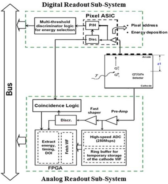
In this paper, we will report on the development of a hybrid pixel-waveform (HPWF) readout system, as seen in Fig. 1, for highly pixelated (with a few hundred μm pitch size) CdTe gamma ray detectors. These crystals were grown by Acrorad Company, Ltd using the Traveling Heater Method (THM). This “Ohmic detector” design offers system stability while being able to operate at a low bias voltage. The designed anode is bump bonded to an application specific integrated circuit (ASIC) based on a modification of the MGC700T2 design developed by Ajat Oy Ltd [41]. This work further builds on the benchtop CdTe detector design reported on by Meng et al. by enabling the HPWF readout method [42].
Fig. 1.
Schematic of the readout circuitry for the HPWF detector. The circuitry is simplified by reducing the burden of the pixelated anode to only report the spatial position of each event. The cathode, on the other hand, is processed for energy, timing and depth of interaction.
This readout system utilizes a pixel readout circuitry connected to the anode pixels, which is designed to provide pixel address only. The pixel circuitry is working in coincidence with a high-speed digitizer to sample the cathode waveform and to provide the energy, timing and DOI information. The justifications for the HPWF readout method are presented as follows. First, the cathode waveform could provide accurate energy information using digital processing techniques that takes into account the effect of charge trapping, different drifting velocities of electrons and holes, and the ballistic deficit introduced by the use of practical pre- and shaping amplifier circuitries. The energy information derived from the cathode is also immune to the charge-loss and charge-sharing effects typically being dominant when the size of the charge-cloud is approaching the physical dimensions of the anode pixels. Second, the cathode waveform could provide timing information at a precision well beyond that available with anode pixel readout. The latter is limited by the intrinsic uncertainties in the charge collection process. Thirdly, this method could also provide reliable DOI information, by measuring the electron drifting time from sampled waveforms. Finally, the HPWF readout system requires a highly simplified circuitry for handling the large number of anode pixels. It will potentially allow one to pack more readout channels per unit area with future generation CMOS ASICs, which could lead to a further improved detector spatial resolution. The proposed HPWF readout system provides a solution for extracting precise spatial, energy and timing information in small-pixel CZT and CdTe detectors for use in future high-performance multi-modality gamma ray imaging systems.
B. Extracting Timing, Energy and DOI Information from the Cathode Waveform
The interactions of gamma rays in CdTe and CZT detectors produce electrons and holes that migrate toward the anode(s) and the cathode under the influence of the electric field. Due to the vast disparity in charge mobility between electrons and holes in CdTe/CZT (1000 cm2/Vs vs. ~100 cm2/Vs), the resulting cathode waveform is naturally partitioned into multiple sections by three bending points: the interaction time, the arrival of electrons at the anode(s), and the arrival of holes at the cathode. The induced charge for a single polarity is defined by Hecht's relationship in Eq. 1 as
| (1) |
where e is the charge of an electron, N0 is the number of initial charge carriers, τf represents the mean-free time of charge carriers, and Tc is the total collection time [43]. Charge trapping is accounted for but de-trapping is not.
An example of an experimentally measured cathode WF is shown in Fig. 2. One could extract the gamma ray interaction time by fitting the measured WF to pre-derived WF models. This approach has been extensively detailed and experimentally validated in our previous work [11][43, 44]. Here, we have used a simplified WF model that treats all the WF sections as linear functions fitted using MATLAB.
Fig. 2.
Cathode waveforms from the CdTe system. (A) Interaction time. (B) Signal induced by electron movement. (C) Electron drifting time. (D) Hole drifting time. (E) Signal induced by electron and hole drifting. Cathode signal one and cathode signal two differ in DOI position. Both cathode waveforms contain very low frequency interference which accounts for the difference in the waveform offset.
In this work, we used a simple approach to extract the energy deposition of gamma ray interactions. We compare the cathode signal amplitudes before the interaction occurred and after all the charge (both electrons and holes) is collected. The difference between these two signal levels is used as an indication of the energy deposition. To compensate for the effect of electron and hole trapping, this signal-difference is multiplied by a correction factor depending on the estimated DOI for each individual gamma ray event. Similar methods have been used extensively for improving the energy resolution in CZT and CdTe detectors [45, 46]. Note that with the measured WF, it would be possible to use many digital signal-processing techniques to extract the energy information [47]. We chose to use this technique because it requires a minimum amount of digital processing and therefore computation, which is desired for high count rates.
Gamma ray interactions occurring at different depths in the detector lead to different electron and hole contributions to the overall cathode signal amplitudes, and different electron and hole drifting times as shown in Fig. 2. These example cathode signals shown in Fig. 2 differ in DOI positional depth if we consider the concepts presented by the Shockley-Ramo theorem presented in Eq. 2 [48].
| (2) |
Again, e is the charge of an electron, N0 is the number of initial charge carriers, but W is the width of the detector and dx represents the displacement of the electron or hole charge carriers. Using this understanding, the total displacement of charge impacts the total amplitude contribution in the waveform. Therefore, the top waveform shown in Fig. 2 indicates that's the electrons must drift from a position very far from the anode while the bottom cathode waveform, dominated by the hole contribution, must drift from a position very close to the anode. While the DOI could be derived using multivariate analyses based on these quantities. For simplicity, we have limited our exploration to the use of various combinations of two parameters only.
C. Prototype Coincidence Detection System Based on Two HPWF Detectors
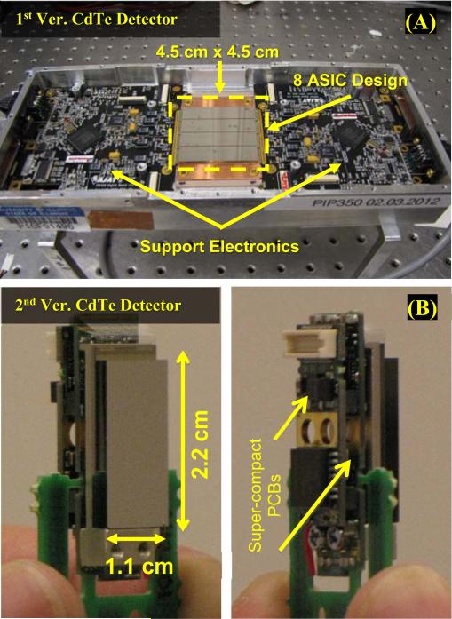
The HPWF detector could be constructed based on multiple versions of the energy resolvable photon counting (ERPC) detectors that are based on the same readout architecture. Fig. 3 shows two versions of our detectors, the second version is an ultra-compact design, which could potentially allow multiple CdTe or CZT based HPWF detectors to form a closely packed ring or other complex geometries. These detectors consist of a varying number of hybrids, ranging from 1 to 8. Each hybrid is composed of a CdTe crystal with a pixelated anode bump-bonded to a 2048 (32 × 64)-channel ASIC to read out the anode pixels. Each pixelated element is 350 μm × 350 μm in size [42].
Fig. 3.
(A) 8 ASIC CdTe detector unit used for experimental procedures. (B) Single ASIC ultra-compact CdTe detector with ultra-compact support electronics. The HPWF detectors used in this study are based on a pair of the bigger detector assembly shown on the top, as this configuration has a more robust housing and the flexibility of setting up using 1-tile-to-1-tile, 2-tile-to-2-tile, 4-tile-to-4-tile coincidence configurations.
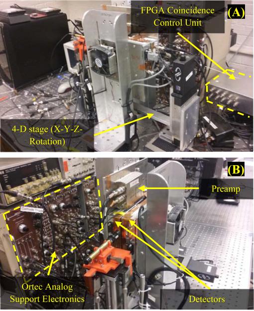
The experimental studies were carried out using two active CdTe hybrids, each being 2.2 cm wide and 1.1 cm long with a thickness of 2 mm, in a benchtop system shown in Fig. 4. The detector firmware was modified to allow coincidence detection, between the two detectors, and a dedicated coincidence control unit was implemented using a Xilinx Spartan FPGA. The readout time per pixel was minimized to 125 ns, and the number of pixels read out on each hybrid was firmware-selectable from 512 to 2048.
Fig. 4.
(A) FPGA coincidence control unit (Xilinx Spartan-3E). The 4-D stage used in the experiments allowed source alignment and the simulation of a multi-detector ring through rotation. (B) Ortec analog shaping and CFD electronics were used to process the Amptek A250 preamplifier signals
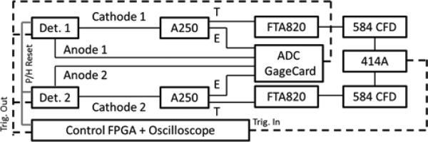
The two HPWF detectors were placed around a 4-D (X-Y-Z-Rotation) stage. Three dimensions were for the translation of the axis of rotation, using Newport motors, so that the selected radioactive source was centered in the system field of view (FOV). The final dimension used a Micronex rotational motor in order to simulate a detector ring. Signals induced in the cathode waveform were shaped with a NIM shaper (Ortec FTA 820) and fed into a constant fraction discriminator (Ortec 584). Events exceeding the threshold were sent to the coincidence unit with a resolving time window of 50 ns. For coincidence events, the cathode signals from both detectors were directed to an external ADC running at 200 M samples/sec. This ADC stored all events in a circular buffer in order to preserve the cathode waveform generated prior to shaped triggering. The schematic of the triggering and readout system are provided in Fig. 5.
Fig. 5.
In the block diagram provided, cathode signals from detector 1 and detector 2 were sent to an Amptek's A250 preamplifier. The waveform was digitized by our Gage ADC while the timing output was shaped by Ortec's FTA820. The shaped ouput was sent to an Ortec 584 constant fraction discriminator (CFD). If the signal arriving at the CFD exceeded 30 mV, a TTL pulse from the CFD would be directed to the Ortec 414a coincident unit. A Xilinx Spartan-3E control FPGA would determine if the coincidence event from the 414a was true or not. Connections between the FPGA and the HPWF PET system were made using P-MOD BNC adapters.
All measurements were performed using a 10 μCi Na-22 point source with a 250 μm diameter. When performing the analysis of the spatial resolution, the point source was rotated to 40 positions with an offset of 1.304 mm to simulate different potential resolutions using 512 active pixels. Each position acquired for a single hour. For the scattering study, a separate 48 angles were imaged for one hour at each position using 1024 active pixels. Detectors were placed at a separation of approximately 27 mm. Most of the measurements were carried out with a bias voltage −300 volts. However, the timing resolution was analyzed under both −300 volts, −400 volts, −500 volts and −750 volts.
D. Lines of Response Data and the Point Source Geometric Calibration
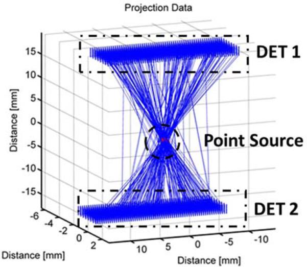
In order to achieve the high spatial resolution desired in our reconstructions, a very precise understanding of the system geometry must be achieved. This was implemented using a point source rotated by fixed increments in a full ring. The resulting line of response (LOR) data is processed and the projections are visualized in MATLAB with a three dimensional representation of our point source, the LOR data, and the system geometry as shown in Fig. 6, with Fig. 6 being an example of our visualization.
Fig. 6.
A 3D example representation of our system geometry for a single angle. Both detectors are modeled here with each individual pixel position plotted. The LOR are plotted and depth is determined from the waveform as previously discussed.
In order to calculate the geometry, we use the built in functions of MATLAB to calculate the geometry with the maximum probability define by the convergence of our LOR data with our point source. The maximization is performed by MATLAB's FMINCON which is shown in Eq. 3.
| (3) |
Here, P is the calcualated probability of the system geometry, and x is a vector which defines the geometric parameters for the point source, the detector one positioning, and the detector two positioning, and dataLOR is the acquired data from a fixed sample angles. The parameters included in x are the offset of the point source from the rotational axis in the x-y-z coordinate system, the origin of the detector positions in the x-y-z coordinate system and the angle of the detectors in the x-y-z coordinate system yielding a total of 15 parameters to describe the system geometry. We use FMINCON to minimize the probability of the geometry through the selection of the parameters present in x given the acquired dataLOR. The probability is determined as a function of the number LORs intersecting the virtual point source. Therefore, once the probability is minimized, the virtual point source sits directly at the point of LOR convergence for every sampled angle. The point source at the position of convergence can be seen in Fig. 6. The parameters in the x vector are determined to be optimal and the geometry is then passed to the reconstruction code in order to ensure a quantitative understand of the object space is achieved.
E. Image Reconstruction and Reconstruction Methods
Image reconstruction contains two steps. One is the high-resolution sinogram rebinning using the 8-DOI information and another one is the iterative reconstruction with positron range correction. Although the detector pixel resolution is 350 μm, a 50 μm resolution in sinogram can be used due to the 8-DOI information [49]. High-resolution sinogram rebinning is computationally efficient in our system because the size of the system matrix using the line of response (LOR) space becomes k2 larger than the size of a conventional system matrix, where k is the number of DOIs. To reduce the size of the system matrix and simplify the geometric model, we create a virtual ring system. The virtual ring system has a single detector layer with a 50 μm resolution and coincides with the first DOI layer on the real system. Although the virtual detector ring significantly reduces the computational complexity, the data sampling in the sinogram space can still be irregular, which could potentially degrade the image quality. Moreover, even though we use isotopes with short positron ranges such as F-18 and Na-22 with 200 and 260 μm full-width-half-maximum (FWHM) [50], the blurring effect can significantly degrade the image quality in our system. To address these challenges, we use a penalized iterative reconstruction algorithm [51] with the Poisson likelihood and the positron range correction that exploits a Gaussian blurring kernel [52] dependent on the isotope and surrounding materials.
Given this reconstruction method and the geometry provided by our calibration, we reconstructed six different images which consider different criteria from the information derived from our HPWF detectors. The first three images consider the raw reconstruction data, reconstruction data with DOI correction, and the reconstruction data with DOI correction and positron range correction. These image are presented as a “synthetic resolution point source image” as a single point source was reconstructed at different positions to determine the system resolution. The second set of three images are only a single point source reconstruction at a single position with a varying number of scattering events to determine the impact on the source distribution.
IV. Experimental Results
A. Depth of Interaction Measurements
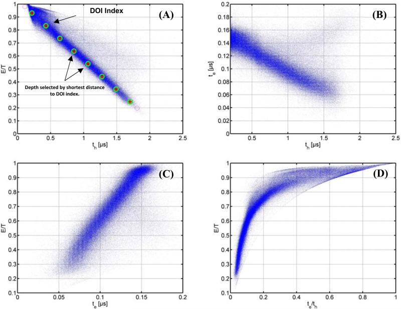
In Fig. 7, we compare several potential options for extracting DOI information from quantities derived from the cathode WF: electron-to-total (E/T) ratio, hole-to-total (H/T) ratio, electron drifting-time (te), hole drifting-time (th).
Fig.7.
(A) Hole drift time vs. the electron amplitude over the total amplitude, (B) Hole drift time plotted against the electron drift time.. (C) Electron drifting time plotted against the ratio of the electron amplitude over the total amplitude, (D) The ratio of electron drift time over hole drift time plotted against the ratio of the electron amplitude over the total amplitude.
These plots generally consist of majority of the data points concentrated around a central band. These are corresponding to events having a single interaction in the detector, and some other data points reside away from the central band resultant from events having multiple interactions.
For the single-interaction events, we anticipated that the narrower the central band is, the better the DOI resolution could be. From this viewpoint, the plot of E/T ratio versus th has the potential of offering the best DOI resolution.
In this study, we used the following procedure to determine DOI. In Fig. 7A, we first fit the central-band into a straight line, and determine the two furthermost ends of the central-band. We assume events falling close to these two end-points are corresponding to gamma ray interactions that happened either close to the cathode side, or close to the anode side. Between the two extreme points, we partition the trend line into multiple (8-32) sections of equal length, and derive the center point of each section as shown in Fig. 6A. To assign a DOI index to each interaction, we further assumed that the DOI is proportional to both the E/T ratio, and to the hole-drifting time (th). For each interaction, if the corresponding plot-point in Fig. 6A is closest to the center of a specific DOI section, the event is assigned to the corresponding DOI bin. Note that is procedure leads to discrete assignment of DOI.
B. Measured Energy Resolution
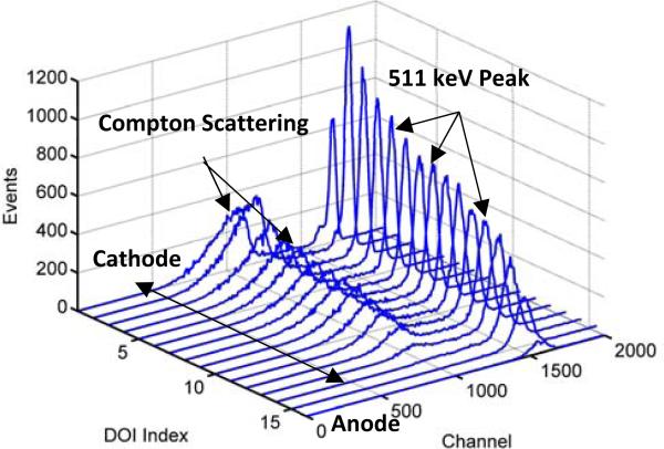
By incorporating the DOI information, we have derived the energy spectra for events detected within 16 DOI bins, as shown in Fig. 8. It is evident that the 511 keV full-energy events are shifted across different DOIs, which is due to the trapping of electrons and holes in the CdTe material.
Fig. 8.
Partitioning the CdTe detector in 16 discrete DOI for the purpose of correcting the energy resolution degradation induced through charge trapping. Lower DOI indices are closer to the cathode.
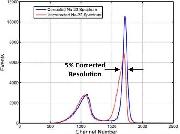
In Fig. 9, we compared the uncorrected overall energy spectrum and the corrected energy spectrum. The overall energy resolution after correction is improved to 5% FWHM at 511 keV, which is significantly better than typical energy resolution for scintillation detectors for PET found to range from 8 – 12% [38]. Furthermore, comparing Fig. 9 to the work of Yongzhi Yin et al. in pixelated energy resolution (of which was reported to be between 9%-11%), it is evident that reading energy information from the cathode side would not only lead to an improved energy resolution, but also to greatly improved peak-to-valley and peak-to-Compton-continuum ratios, which warrants a greatly improved capability of rejecting scattered gamma rays, as well as offers an improved effective detection efficiency when a finite low-energy threshold is used [27].
Fig. 9.
The red spectrum is the DOI uncorrected energy spectrum. The blue spectrum is the result of correcting for the charge loss observed in the DOI partitioned spectrum. The final result is an energy resolution of 5%.
It is important to note that the energy resolution obtained from the cathode waveform is independent of the pixilation of the anode, and will not be affected by the use of even small pixel sizes, and by the charge sharing and charge loss processes associated with anode pixels. Therefore the HPWF approach provides a simple approach for achieving an excellent energy resolution for highly pixelated semiconductor detectors.
For the purpose of understanding the implications of the HPWF cathode amplitude spectrum, single stage CR-RC shaping was performed as well. CR-RC shaping was performed by the convolution of the cathode WF with CR-RC filter function shown as,
| (4) |
where WF(t) is the experimentally measured cathode waveform in the time domain and Flt(t)CR–RC is the single stage shaping filter. The semi-Gaussian filter is defined in Eq. 5. In our work, analysis was performed using a single shaping value with τ1 = τ2 = τ and defining t as time. Utilizing equal values, the single stage filter is defined as,
| (5) |
where multiple shaping times were selected to perform a comparative analysis.
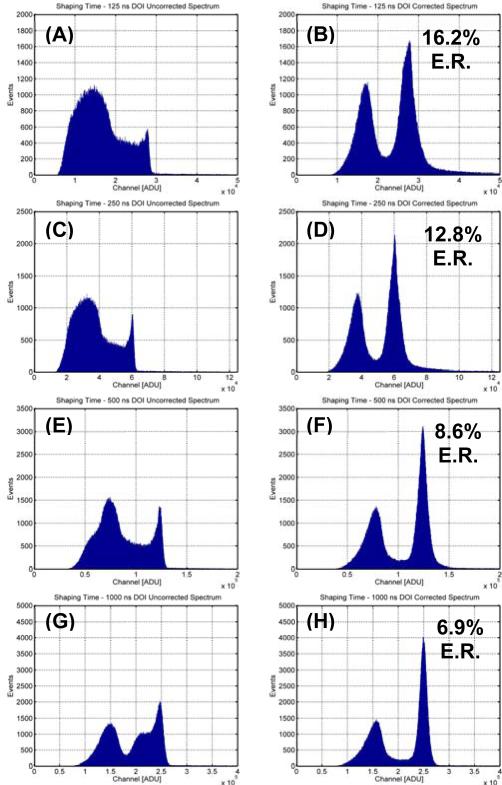
The single stage CR-RC cathode shaping analysis resulted in spectra, shown in Fig. 10, which were poorer in resolution than the cathode amplitude method, shown in Fig 8. For a 125 ns shaping time, the FWHM results in an energy resolution of only 16.2%. Further increases in shaping time to 250 ns, 500 ns, and 1000 ns show an energy resolution of 12.8%, 8.6% and 6.9% after DOI correction, respectively. Ultimately, the data from the cathode non-shaping prove to be superior. Single stage shaping did not show improvements over the raw cathode energy amplitude resolution of 5%.
Fig. 10.
Subfigures A, C, E, and G show the DOI uncorrected shaped spectra collected form 125ns, 250ns, 500 ns, and 1000 ns shaping times, respectively. Subfigures B, D, F, and H are the DOI corrected figures used to derive the energy resolution for each separate shaping time.
C. Measured Timing Resolution
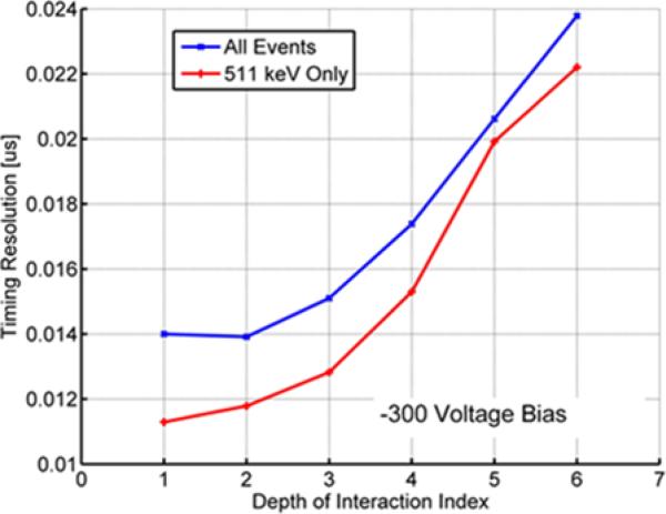
The potential implementation of the HPWF detector design in PET imaging required the measurement of the timing resolution of the system. Experimental results for −300 volts showed a timing resolution of 17.5 ns. Given the thickness of the CdTe detector, DOI based considerations were given to the timing resolution. Under DOI conditions, each detector was partitioned into 6 DOI indices. In this analysis, the timing resolution was derived from coincidence events in the same respective DOI index for each detector. The results of DOI analysis for −300 volts are shown in Fig. 11. Here, the data is considered in terms of the full energy spectrum as well as only the 511 keV events. When considering the full energy spectrum, the best timing resolution is achieved when only the first DOI of both detectors is used. This yields the best timing at 14 ns with the tradeoff of detector thickness. When considering only 511 keV events, the best timing resolution is again achieved in the first DOI of both detectors. The timing resolution is pushed to as low as 11 ns.
Fig.11.
DOI partitioned timing resolution for −300 volts for the full energy spectrum and just the 511 keV photopeak events.
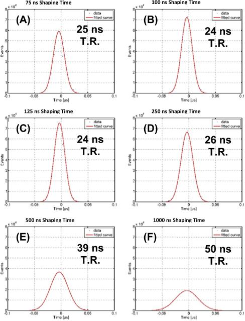
The waveforms acquired from the −300 volt condition were also shaped in order to determine if fitting could potentially provide a desired improvement. The timing resolution derived from the single stage shaping did not result in a timing resolution competitive to scintillation based coincidence systems nor did it show superiority to the fitted cathode condition. Selected shaping times ranged from 75 ns to 1000 ns, results are shown in Fig. 12. Timing resolution, defined by the FWHM of the shaped distribution, was measured to 25 ns, 24 ns, 24 ns, 26 ns, 39 ns and 50 ns for shaping times of 75 ns, 100 ns, 125 ns, 250 ns, 500 ns and 1000 ns respectively. Timing resolution was optimized under 250 ns as further reduction in shaping time proved to provide no further improvements.
Fig. 12.
Timing resolution as a result of shaping times selected as 75 ns, 100 ns, 125 ns, 250 ns, 500 ns, and 1000 ns, respectively.
Additional, high voltage settings were also considered for waveform fitting. Varying the high voltage applied to the system from −400 volts, −500 volts and −750 volts showed only some improvement. The timing resolution improved to 16.81 ns, 16.71 ns and 14.66 ns respectively. This analysis was done for the full energy spectrum with no specific analysis done for 511 keV as a function of DOI.
D. Preliminary Point Source Synthetic Spatial Resolution Reconstruction
The synthetic resolution point source image was reconstructed under 3 different condition: (a) the raw image with no consideration toward DOI and positron range correction, (b) the reconstructed point source with depth of interaction considered in the reconstruction but no consideration applied toward positron range, and (c) the final image with both DOI correction applied and positron range applied. The conditions are presented in Fig. 13.
Fig. 13.
(A) Point source with no corrections considered for DOI and positron range. (B) DOI corrections applied to the reconstruction. (C) Final image with corrections applied for positron range and DOI. Each condition is complemented by its respective profile. The profile itself runs along the center of all the point sources present in the reconstruction.
In order to demonstrate the potential resolution of the system, multiple reconstruction so of the same point source were superimposed on the same image with varying separations to create our synthetic resolution point source image. The first distance between point sources was approximately 300 μm and every following point source had an increase in separation by 50 μm (maximum separation in the image was limited to 450 μm). The absence of any corrections shown in Fig. 13A did not produce clear separation of any selected distanced and showed no potential for resolving the 300 μm separation. Implementing DOI correction in Fig. 13B showed a clear improvement in the point source shape and the resolvability of the initial 300 μm point source separation. Correcting for DOI and positron range in Fig. 13C showed the clear resolvability of the 300 μm.
E. A Quantitative Study of the Inter-Pixel Compton Scattering
The densities and effective atomic numbers (Zeff) of CdTe and CZT materials (~50 and 5.85 g/cm3 for CdTe, ~49 and 5.78g/cm3 for CZT) are substantially lower than those for common scintillation materials, such as LSO (66, 7.4g/cm3), BGO (74, 7.13g/cm3) and GSO (59, 6.71g/cm3). For the potential use of CZT or CdTe detectors for PET applications, we have experimentally studied the effect of Compton scattering of 511 keV gamma rays in the relatively thin CdTe detectors. The analysis of the impact of Compton scattering is presented in Fig. 14 and Fig. 15.
Fig. 14.
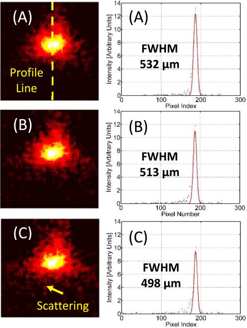
Vertical point source profile. All events use DOI information but do not use positron range correction. (A) A single point source reconstruction using no events classified as scattered. (B) A single point source reconstruction with 500 single interaction events and 500 multiple interaction events per angle of 48 angles. (C) 1000 multiple interaction events per angle point source reconstruction.
Fig. 15.
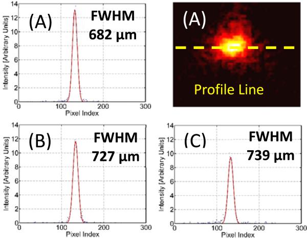
Horizontal point source profile. All events use DOI information but do not use positron range correction. (A) A single point source reconstruction using no events classified as scattered. (B) A single point source reconstruction with 500 single interaction events and 500 multiple interaction events per angle of 48 angles. (C) 1000 multiple interaction events per angle point source reconstruction.
A single dataset utilizing the 1024 active pixel condition was partitioned into subsets which were composed of different ratios of events identified as single interaction and multiple interaction. These events were categorized by computationally shaping the cathode waveform digitized from readout in post processing to identify single cathode interactions with multiple non-adjacent position active anode events. The raw data set showed only 70% of the events to be of single interaction (compared to the 90% condition of the 512 active pixel experiment). The horizontal and vertical point source profiles were analyzed for their potential impact on resolution. In Fig. 14, three different ratios were used in reconstructing the point source. Fig. 14A looks at the vertical profile of the point source which yields a 532 μm FWHM. Increasing the fraction to 500 multiple interaction events per angle to 1000 multiple interaction events (of 1000 events used per angle) resulted in a FWHM of 513 μm and 498 μm as shown in Fig. 14B and 14C.
In Fig. 15, the same three ratios are provided with the horizontal profile of the point source distribution and the resulting reconstruction. DOI corrections were included but positron range was not for all figures. Fig 15A shows the results of a reconstruction without any events classified as scattering events yielding a FHWM of 682 μm. Fig 15B shows the resulting profile if half the events were identified as scattering events which results in a FWHM of 727 μm. In Fig. 15C, the final condition, only events were identified as scattered events were included in the reconstruction showing that the FWHM degraded even further to 739 μm thus indicating that resolution can be manipulated through selecting different ratios of scattered and non-scattered events.
V. Discussion
The implementation of the combined cathode waveform with the spatial information from the pixelated anode of our CdTe detector has allowed for simple circuitry to extract DOI indexed positioning while alleviating some of the challenges associated with the use of semiconductor detectors. In this work, analysis, in the context of DOI indexing, was performed on the energy, timing resolution and spatial resolution in order to evaluate the feasibility of HPWF CdTe detectors in PET and SPECT studies.
The direct measurement of the energy resolution from the cathode waveform showed the impact of charge trapping in the crystal. In order to correct for the hole tailing, the identified DOI method was used to partition data and implement a correction to achieve a 5% energy resolution for 511 keV. The DOI indexing and the depth-used partitioning of the energy spectra yielded the desired energy resolution and is easily implemented in each detector independently. Comparatively, the DOI-corrected shaped spectra achieved energy resolutions of 16.2%, 12.8%, 8.6% and 6.9% for the selected shaping times.
However, experimental data for the system timing resolution proved challenging given the 17.52 ns achieved using a −300 volt bias. The increase in the bias, as high as −750 volts did not bring a significant improvement in the timing resolution which was contrary to expectations. Upon closer inspection, the leakage current for -300 volts, −400 volts, −500 volts and −750 volts proved to be significant. The summed leakage current across both preamps was 0.002 mA, 0.003 mA, 0.004 mA and 0.007 mA for the aforementioned settings which would explain for the small improvement as a function of the high voltage setting as an increase in leakage current reduces the effective bias applied at the detector crystal. It should be noted that while the timing resolution did not improve dramatically with voltage, the DOI analysis indicates that crystal thickness as well as the deposited energy play a significant role in the systems timing resolution. Selecting only 511 keV events with a rather thin CdTe crystal could lead to 11 ns timing resolution, or better, resulting in a smaller gap between semiconductor and scintillator detection systems but not necessarily an equivalent order of magnitude. Shaped timing resolution proved to be worse than the fitted cathode waveform with the best timing achieved under a 250 ns shaping time. However, this timing resolution was only 25 ns compared to the cathode fitted resolution of 17.52 ns.
As one may have noticed, the timing resolution that we are reporting in this paper are relatively poor compared to those achievable with state-of-art scintillation detectors. We have previously derived the theoretical limit on timing resolution attainable from thick (5 mm to 1 cm) semiconductor detectors through waveform fitting approaches, and carried out a careful experimental study to verify the theoretical limits [43][44]. The current timing measurement was carried out using a prototype detector for demonstrating the HPWF detector concept, there are clearly room for further improve the timing resolution by applying higher bias to speed up the electron and hole movement in the detector, by segmenting the cathode to reduce the electronic noise so that to reduce the uncertainty on the estimated interaction time. These could be an important topic in our future research. In addition, as we pointed out, we are developing the HPWF detector as a general gamma ray imaging detector, so there could be many applications that do not require an excellent timing resolution
In terms of spatial resolution, the preliminary point source reconstruction outperforms scintillation imaging systems. In the absence of any corrections, the system showed potential for sub-millimeter resolution. The inclusion of DOI correction led to the breach of the 500 μm resolution limit, and the inclusion of positron range correction made 300 μm clearly resolvable indicating that sub-300 μm might even be possible. However, it should be understood that a point source is a rather simple imaging condition. Further, more complex imaging studies must be performed.
The HPWF method, which is able to discern between scattered and non-scattered interactions, provided fundamental insight into the impact of scattered events into the system performance, a criteria which needs to be understood due to the low effective Z of CdTe. It should be understood that only a fraction of the detector was readout (1024 pixels of the 2048 pixels). Given this, there is potential for some the events used in the reconstruction to be misidentified, especially at the boundary of the active anode and the inactive anode region. The work here had 90% of all events in the 512 condition identified as single interaction, and only 70% identified as single interaction under the 1024 condition. Future work must look closer at the impact of the full detector usage.
The results show an improvement in the horizontal resolution with less scattering events, and a degradation in the vertical profile with fewer scattering events. The change in the horizontal profile is improved by 57 μm and the vertical profile degrades by 34 μm. It is anticipated that the resolution should degrade with increased scattering. While the reasoning for the improvement in one direction over another is not understood, it can be assumed that a quantifiable change is present but the resulting data does not clearly indicate the potential improvement in resolution.
The final discussion lies in the difference in resolution obtained between the synthetic resolution point source image and the inter-pixel scattering section. The first obvious statement is that the final section does not account for the positron range correction implemented in the synthetic resolution point source image. The second condition that should be considered is the use of the different partial active regions on the detector anode. The fundamental fraction of single events present shifts from 90% for 512 to 70% for 1024 indicating that some multiple interaction events may be scattering into the inactive detector leaving the scattering event as the recorded spatial position. This would result in the correct anode interaction position being recorded as potentially correct. Regardless, the resolution of the system can be further verified with a simple resolution phantom study.
The reassurance of the high spatial resolution achievable with the HPWF CdTe detectors does bring a single discrepancy. The DOI partitioning is achieved without consideration (or at least not direct discussion) of the numerical depth achieved within the detector. DOI is discussed in the context of detector depth index and not absolute position. Adding a physical position to the DOI information is critical in achieving a precise understanding of the resolution improvement provided by the cathode DOI extraction method.
Detector sensitivity was not discussed in this paper. However, there are a few points which should be made regarding the current detector functionality. Only single cathode events can be identified during readout. Therefore, if multiple events in the cathode are detected the event must be thrown away in post processing. While this hinders sensitivity of this detector, engineering modifications can be further made. Considerations have been made toward partitioning the cathode in smaller sections will help improve the detector count rate through the rejection of fewer events, increasing the system bias to improve event separation, and implementing pile-up rejection algorithms in post processing. This is another step which we intend to take with this detector design.
VI. Conclusions
HPWF CdTe detectors showed that the combination of the cathode waveform with the anode allows the alleviation of various perceived shortcomings of semiconductor-based detectors for application in small animal PET and SPECT. Given the ability to derive relative DOI, corrections in both energy and spatial resolution were achievable. While the timing resolution for potential PET applications appears at first to be poor, timing resolution viewed in terms of depth and energy shows that better resolution can be achieved when compared to shaping data. This preliminary analysis supports the application of HPWF CdTe detectors in PET and SPECT systems.
Contributor Information
A. Groll, Nuclear, Plasma, and Radiological Engineering, University of Illinois at Urbana-Champaign, IL 61801 USA (primary: groll1@illinois.edu).
K. Kim, Massachusetts General Hospital and Harvard Medical School, Boston, MA 02114 USA
H. Bhatia, Nuclear, Plasma, and Radiological Engineering, University of Illinois at Urbana-Champaign, IL 61801 USA
J. C. Zhang, Nuclear, Plasma, and Radiological Engineering, University of Illinois at Urbana-Champaign, IL 61801 USA
J. H. Wang, Nuclear, Plasma, and Radiological Engineering, University of Illinois at Urbana-Champaign, IL 61801 USA
Z. M. Shen, Nuclear, Plasma, and Radiological Engineering, University of Illinois at Urbana-Champaign, IL 61801 USA
L. Cai, Nuclear, Plasma, and Radiological Engineering, University of Illinois at Urbana-Champaign, IL 61801 USA
J. Dutta, Massachusetts General Hospital and Harvard Medical School, Boston, MA 02114 USA
Q. Li, Massachusetts General Hospital and Harvard Medical School, Boston, MA 02114 USA (Li.Quanzheng@mgh.harvard.edu).
L. J. Meng, Nuclear, Plasma, and Radiological Engineering, University of Illinois at Urbana-Champaign, IL 61801 USA
REFERENCES
- 1.Cherry SR, et al. MicroPET: a high resolution PET scanner for imaging small animals. IEEE Transactions on Nuclear Science. 1997 Jun;44(3):1161–1166. [Google Scholar]
- 2.Schramm N, Wirrwar A, Sonnenberg F, Halling H. Compact high resolution detector for small animal SPECT. IEEE Transactions on Nuclear Science. 2000 Jun;47(3):1163–1167. [Google Scholar]
- 3.Beekman FJ, Have F, Vastenhouw B, et al. U-SPECT-I: a novel system for submillimeter-resolution tomography with radiolabeled molecules in mice. Journal of Nuclear Physics. 2005;46:1194–1200. [PubMed] [Google Scholar]
- 4.Liu Ted, Clinthorne Neal, Cochran Eric, Chesi Enrico, Grkovski Milan, Grošičar Borut, Honscheid Klaus, Huh Sam S., Kagan Harris, Lacasta Carlos, Brzezinski Karol, Linhart Vladimir, Mikuž Marko, Shane Smith D, Stankova Vera, Studen Andrej, Weilhammer Peter, Žontar Dejan. A High-Resolution PET Demonstrator using a Silicon “Magnifying Glass”. Proceedings of the 2nd International Conference on Technology and Instrumentation in Particle Physics (TIPP 2011), Physics Procedia. 2012;37:1488–1496. doi: 10.1016/j.phpro.2012.03.747. [DOI] [PMC free article] [PubMed] [Google Scholar]
- 5.Matteson JL, et al. IEEE Nuclear Science Symposium Conference Record. Dresden; Germany: 2008. 2008. Charge collection studies of a high resolution CZT-based detector for PET; pp. 503–510. [Google Scholar]
- 6.Ariño G, et al. Energy and coincidence time resolution measurements of CdTe detectors for PET. Physics in Medicine and Biology. 2013;8 doi: 10.1088/1748-0221/8/02/C02015. [DOI] [PMC free article] [PubMed] [Google Scholar]
- 7.Yang Y, et al. A high resolution prototype small-animal PET scanner dedicated to mouse brain imaging. Journal of Nuclear Medicine. 2016 Mar; doi: 10.2967/jnumed.115.165886. [DOI] [PMC free article] [PubMed] [Google Scholar]
- 8.Scheiber C, Giakos G. Medical applications of CdTe and CdZnTe detectors. Nuclear Instruments and Methods in Physics Research A. 2001 Feb;458:12–25. [Google Scholar]
- 9.Sheiber C. CdTe and CdZnTe detectors in nuclear medicine. Nuclear Instruments and Methods in Physics Research A. 2000 Jul;448:513–524. [Google Scholar]
- 10.Accorsi R, et al. MediSPECT: Single photon emission computed tomography system for small field of view small animal imaging based on a CdTe hybrid pixel detector. Nuclear Instrumentations and Methods in Physics Research A. 2007 Feb;571:44–47. [Google Scholar]
- 11.Cai L, Meng L-J. Hybrid pixel-waveform CdTe/CZT detector for use in an ultrahigh resolution MRI compatible SPECT System. Nuclear Instruments and Methods in Physics Research A. 2013 Aug;702:101–103. doi: 10.1016/j.nima.2012.08.069. [DOI] [PMC free article] [PubMed] [Google Scholar]
- 12.Cai L, et al. MRC-SPECT: A sub-500 μm resolution MR-compatible SPECT system for simultaneous dual-modality study of small animals. Nuclear Instruments and Methods in Physics Research A. 2013 Sep;734:147–151. doi: 10.1016/j.nima.2013.08.080. [DOI] [PMC free article] [PubMed] [Google Scholar]
- 13.Park S-J, et al. Evaluation of quantitative accuracy in CZT-based pre-clinical SPECT for various isotopes. Jinst. 2015 May;10 [Google Scholar]
- 14.Mitchell G, et al. CdTe Strip Detector Characterization for High Resolution Small Animal PET. IEEE Transactions on Nuclear Science. 2008 Jun;55(3):870–876. [Google Scholar]
- 15.Morimoto Y, et al. Development of a 3D Brain PET scanner Using CdTe Semiconductor Detectors and Its First Clinical Application. IEEE Transactions on Nuclear Science. 2011 Oct;58(5):2181–2189. [Google Scholar]
- 16.Shiga T, et al. A New PET Scanner with Semiconductor Detectors Enables Better Identification of Intratumoral Inhomogeneity. J Nucl Med. 2009 Jan;50(1):148–155. doi: 10.2967/jnumed.108.054833. [DOI] [PubMed] [Google Scholar]
- 17.Ueno Y, et al. Basic Performance Test of a Prototype PET Scanner Using CdTe Semiconductor Detectors. IEEE Transactions on Nuclear Science. 2009 Feb;56(1):24–28. [Google Scholar]
- 18.et al J-GM-M. Toward VIP-PIX: A Low Noise Readout ASIC for Pixelated CdTe Gamma-Ray Detectors for Use in The Next Generation of PET Scanners. IEEE Transactions on Nuclear Science. 2013 Aug;60(4):2898–2904. doi: 10.1109/TNS.2013.2270115. [DOI] [PMC free article] [PubMed] [Google Scholar]
- 19.Mikhaylova E, et al. Simulation of the Expected Performance of a Seamless Scanner for Brain PET Based on Highly Pixelated CdTe Detectors. IEEE Transactions on Medical Imaging. 33(2):332–339. doi: 10.1109/TMI.2013.2284657. [DOI] [PMC free article] [PubMed] [Google Scholar]
- 20.Yin Y, et al. Evaluation of PET Imaging Resolution Using 350 μm Pixelated CZT as a VP-PET Insert Detector. IEEE Transactions on Nuclear Science. 2014 Feb;61(1):154–161. [Google Scholar]
- 21.Cai Liang, Lai Xiaochun, Shen Zengming, Chen Chin-Tu, Meng Ling-Jian. MRC-SPECT: A sub-500 μm resolution MR-compatible SPECT system for simultaneous dual-modality study of small animals, Nuclear Instruments and Methods in Physics Research Section A: Accelerators, Spectrometers, Detectors and Associated Equipment. 2014 Jan 11;734(Part B):147–151. doi: 10.1016/j.nima.2013.08.080. [DOI] [PMC free article] [PubMed] [Google Scholar]
- 22.Kubo N, Zhao S, Fujiki Y, Kinda A, Motomura N, Katoh C, Shiga T, Kawashima H, Kuge Y, Tamaki N. Evaluating performance of a pixel array semiconductor SPECT system for small animal imaging. Ann. Nucl. Med. 19(7):633–639. doi: 10.1007/BF02985059. 200. [DOI] [PubMed] [Google Scholar]
- 23.Takahashi T, Watanabe S. Recent progress in CdTe and CdZnTe detectors. IEEE Transactions on Nuclear Science. 2001 Aug;48(4):950–959. [Google Scholar]
- 24.Gu Y, et al. Study of high-resolution, 3-D positioning cadmium zing telluride detector for PET. Physics in Medicine and Biology. 2011;56:1563–1584. doi: 10.1088/0031-9155/56/6/004. [DOI] [PMC free article] [PubMed] [Google Scholar]
- 25.Manook A, et al. Small-Animal PET Imaging of Amyloid-Beta Plaques with [11C]PiB and Its Multi-Modal Validation in an APP/PS1 Mouse Model of Alzheimer's Disease. PLoS ONE. 2012 Mar;7(3) doi: 10.1371/journal.pone.0031310. [DOI] [PMC free article] [PubMed] [Google Scholar]
- 26.Snellman A, et al. In vivo PET imaging of beta-amyloid deposition in mouse models of Alzheimer's disease with a high specific activity PET imaging agent [18F]flutemetamol. EJNMMI Research. 2014 Dec;4(1) doi: 10.1186/s13550-014-0037-3. [DOI] [PMC free article] [PubMed] [Google Scholar]
- 27.Yin Y, et al. 3-D Spatial Resolution of 350 μm Pitch Pixelated CdZnTe Detectors for Imaging Applications. IEEE Transactions on Nuclear Science. 2013 Feb;60(1):9–15. doi: 10.1109/TNS.2012.2213611. [DOI] [PMC free article] [PubMed] [Google Scholar]
- 28.Yin Y, et al. Characterization of Highly Pixelated CZT Detectors for Sub-millimeter PET Imaging. IEEE Nuclear Science Symposium Conference Record. 2009 Nov;:2411–2414. [Google Scholar]
- 29.Bolotnikov AE, Cook WR, Harrison FA, Wong AS, Schindler SM, Eichelberger AC. Charge loss between contacts of CdZnTe pixel detectors. Nuclear Instruments and Methods in Physics Research Section A: Accelerators, Spectrometers, Detectors and Associated Equipment. 1999;432:326–331. [Google Scholar]
- 30.Gu Y, Levin CS. Study of electrode pattern design for a CZT-based PET detector. Phys. Med. Biol. 2014 May;59(11) doi: 10.1088/0031-9155/59/11/2599. [DOI] [PMC free article] [PubMed] [Google Scholar]
- 31.He Z, Knoll GF, Wehe DK, Miyamoto J. Position-sensitive single carrier CdZnTe detectors. Nuclear Instruments & Methods in Physics Research Section a-Accelerators Spectrometers Detectors and Associated Equipment. 1997 Mar 21;388:180–185. [Google Scholar]
- 32.Ballabriga R, et al. Characterization of the Medipix3 pixel readout chip. JINST. 2011 Jan;6 [Google Scholar]
- 33.Ballabriga R, et al. The Medipix3RX: a high resolution, zero dead-time pixel detector readout chip allowing spectroscopic imaging. JINST. 2013 Feb;8 [Google Scholar]
- 34.Ponchut C, et al. SMARTPIX, a photon-counting pixel detector for synchrotron applications based on Medipix3RX readout chip and active edge pixel sensors. JINST. 2015 Jan;10 [Google Scholar]
- 35.Suzuki K, Seto S, Sawada T, Imai K. Carrier transport properties of HPB CdZnTe and THM CdTe:Cl. Proc. IEEE Nucl. Sci. Symp. Conf. Rec. 2001;4:2391–2395. [Google Scholar]
- 36.Eisen Y, Shor A. CdTe and CdZnTe materials for room-temperature X-ray and gamma ray detectors. J. Crystal Growth. 1998 Feb;184/185:1302–1312. [Google Scholar]
- 37.Cates J, Levin C. Advances in coincidence time resolution for PET. Physics in Medicine and Biology. 2016 Feb;61:2255–2264. doi: 10.1088/0031-9155/61/6/2255. [DOI] [PubMed] [Google Scholar]
- 38.Moses WW. Recent advances and future advances in time-of-flight PET. Nuclear Instruments and Methods in Physics Research A. 2007 Oct;580(2):919–924. doi: 10.1016/j.nima.2007.06.038. [DOI] [PMC free article] [PubMed] [Google Scholar]
- 39.Vandenberghe S, et al. Recent developments in time-of-flight PET. EJNMMI Physics. 2016;3(3) doi: 10.1186/s40658-016-0138-3. [DOI] [PMC free article] [PubMed] [Google Scholar]
- 40.Szeles C. CdZnTe and CdTe materials for X-ray and gamma ray radiation detector applications. phys. stat. sol. 2004 Feb;241(3):783–790. [Google Scholar]
- 41.Spartiotis K, et al. A photon counting CdTe gamma- and X-ray camera. Nuclear Instruments and Methods in Physics Research A. 2005;550:267–277. doi: 10.1016/j.nima.2009.02.043. [DOI] [PMC free article] [PubMed] [Google Scholar]
- 42.Meng L-J, et al. Preliminary evaluation of a novel energy-resolved photon-counting gamma ray detector. Nuclear Instruments and Methods in Physics Research A. 2009 Jun;604(3):548–554. doi: 10.1016/j.nima.2009.02.043. [DOI] [PMC free article] [PubMed] [Google Scholar]
- 43.Meng L-J, He Z. Exploring the limiting timing resolution for large volume CZT detectors with waveform analysis. Nuclear Instruments and Methods in Physics Research A. 2005 Sep;550(1-2):435–445. doi: 10.1016/j.nima.2005.04.076. [DOI] [PMC free article] [PubMed] [Google Scholar]
- 44.Meng L-J, He Z. Estimate interaction timing in a large volume HgI2 detector using cathode pulse waveforms. Nuclear Instruments and Methods in Physics Research A. 2005 Jun;545(1-2):234–251. doi: 10.1016/j.nima.2005.01.323. [DOI] [PMC free article] [PubMed] [Google Scholar]
- 45.He Z, et al. 1-D position sensitive single carrier semiconductor detectors. Nuclear Instrumetns and Methods in Physics Research A. 1996 Oct;380(1-2):228–231. [Google Scholar]
- 46.He Z, et al. Position-sensitive single carrier CdZnTe detectors. Nuclear Instruments and Methods in Physics Research A. 1997 Mar;388(1-2):180–185. [Google Scholar]
- 47.Meng L-J. Spectroscopic Performance of Thick HgI2 Detectors. IEEE Transactions on Nuclear Science. 2006 Jun;53(3):1706–1712. doi: 10.1109/TNS.2006.873714. [DOI] [PMC free article] [PubMed] [Google Scholar]
- 48.Knoll Glenn F. Radiation Detection and Measurement. 4th Edition. John Wiley & Sons; 2010. [Google Scholar]
- 49.Kim K, Dutta J, Groll A, El Fakhri G, Meng L-J, Li Q. Proceedings, 13th International Meeting on Fully Three-Dimensional Image Reconstruction in Radiology and Nuclear Medicine. RI. Newport: May 31 4, Jun 31 4, 2015. Penalized maximum likelihood reconstruction of ultrahigh resolution PET with depth of interaction. [Google Scholar]
- 50.Alessio AM, Stearns CW, Tong S, Ross SG, Kohlmyer S, Ganin A, Kinahan PE. Application and evaluation of a measured spatially variant system model for PET image reconstruction. IEEE Transactions on Medical Imaging. 2010;29(3):938–949. doi: 10.1109/TMI.2010.2040188. [DOI] [PMC free article] [PubMed] [Google Scholar]
- 51.Kim K, Dutta J, Groll A, El Fakhri G, Meng L-J, Li Q. Penalized maximum likelihood reconstruction of ultrahigh resolution PET with depth of interaction. International Meeting on Fully Three-Dimensional Image Reconstruction in Radiology and Nuclear Medicine. 2015:296–299. [Google Scholar]
- 52.Bai B, Ruangma A, Laforest R, Tai Y-C, Leahy RM. IEEE Nuclear Science Symposium. Vol. 4. IEEE; 2003. Positron range modeling for statistical PET image reconstruction; pp. 2501–2505. [Google Scholar]


