

Abstract
We investigate the formation of extended defects during molecular-dynamics (MD) simulations of GaN and InGaN growth on (0001) and () wurtzite-GaN surfaces. The simulated growths are conducted on an atypically large scale by sequentially injecting nearly a million individual vapor-phase atoms towards a fixed GaN surface; we apply time-and-position-dependent boundary constraints that vary the ensemble treatments of the vapor-phase, the near-surface solid-phase, and the bulk-like regions of the growing layer. The simulations employ newly optimized Stillinger-Weber In-Ga-N-system potentials, wherein multiple binary and ternary structures are included in the underlying density-functional-theory training sets, allowing improved treatment of In-Ga-related atomic interactions. To examine the effect of growth conditions, we study a matrix of >30 different MD-growth simulations for a range of InxGa1-xN-alloy compositions (0 ≤ x ≤ 0.4) and homologous growth temperatures [0.50 ≤ T/T*m(x) ≤ 0.90], where T*m(x) is the simulated melting point. Growths conducted on polar (0001) GaN substrates exhibit the formation of various extended defects including stacking faults/polymorphism, associated domain boundaries, surface roughness, dislocations, and voids. In contrast, selected growths conducted on semi-polar () GaN, where the wurtzite-phase stacking sequence is revealed at the surface, exhibit the formation of far fewer stacking faults. We discuss variations in the defect formation with the MD growth conditions, and we compare the resulting simulated films to existing experimental observations in InGaN/GaN. While the palette of defects observed by MD closely resembles those observed in the past experiments, further work is needed to achieve truly predictive large-scale simulations of InGaN/GaN crystal growth using MD methodologies.
I. INTRODUCTION
Solid-state lighting (SSL) has begun to broadly replace conventional light sources, thereby reaping tremendous economic and environmental benefits through increased energy efficiency;1–5 however, the “green gap”6 in SSL efficiency remains a major hurdle in this technological transformation. In particular, high-efficiency red, green, and blue (RGB) light emitters are needed to use color mixing in order to assemble the white light most suitable for human eyes and to eliminate phosphor-down-conversion losses that limit the efficiency of present-day commercial SSL technology. While high efficiencies have been achieved for blue (using InGaN alloys) and red light (using AlGaInP alloys), these alloys' emission efficiency is significantly lower for the green-to-yellow light needed for color-mixing approaches to SSL. This green gap cannot be filled by AlGaInP alloys because the alloy transitions to an indirect band gap at the necessary compositions. InGaN alloys, on the other hand, remain as direct-gap semiconductors when tuned to the green spectral range (and beyond) by increasing the alloy's indium content. Despite the extensive studies, however, an abrupt reduction in quantum efficiency occurs for InxGa1-xN emitting at blue-green wavelengths longer than ∼500 nm, which corresponds to increasing indium compositions beyond x ∼ 0.2.7
This drop in quantum efficiency in conventional InGaN-alloy films has been attributed to multiple underlying mechanisms including8–15 (a) misfit-dislocation formation driven by lattice mismatch, (b) spinodal-like decomposition driven by thermodynamic immiscibility, (c) poor electron-hole wavefunction overlap driven by piezoelectric and spontaneous polarization, and (d) point-defect incorporation driven by low growth temperatures. These mechanisms all worsen as the In composition increases because the corresponding lattice-mismatch strain increases and the required InGaN-growth temperature decreases. While experiments to improve planar-alloy growth continue, nanostructured-alloy growth has increasingly entered the research arena. The three-dimensional elastic response enabled by nanostructuring provides a new degree of freedom unavailable to conventional planar heteroepitaxy, with the potential to improve the optical performance of nanostructured-InGaN devices.9,16–19 In particular, InGaN nanowires with 40% or more indium incorporation and reduced defect densities have been achieved,16,17 and the synthesis of InxGa1-xN nanowires across the entire composition range from x = 0 to 1 has been reported.20 Nanowire growth, however, introduces new structural complexity where compositions, stresses, and defect-formation processes simultaneously couple to the nanostructure's shape evolution.17
To complement these ongoing experimental efforts to improve InGaN alloys, the present work uses molecular dynamics (MD) to directly simulate large-scale (∼800 000 atoms), open-system, InGaN-alloy growth onto planar (0001) and () GaN substrates. The simulations model a range of InxGa1-xN-alloy compositions 0 ≤ x ≤ 0.4 and homologous growth temperatures 0.50 ≤ T/T*m(x) ≤ 0.90, where T*m(x) is the simulated melting point of the particular composition. We perform atomistic analyses of the defects formed in the MD-simulated epitaxial structures and compare the results of defects in GaN and InGaN alloys with the previous studies.
Existing MD simulations of InGaN growth21–23 and GaN growth24–32 have typically considered smaller systems, containing fewer than ∼20 000 atoms, consistent with their focus on either nanoscale or atomistic processes. Examples include the studies of interfacial bonding,21 bulk-nanoclustering,22 quantum-dot self-assembly,23 surface diffusion,27 interfacial crystallization,29 and adatom absorption/desorption.31 Since these small systems cannot capture the formation of the larger extended defects observed herein, we will primarily compare our MD simulations to the results selected from the extensive literature experimental studies of defects for both GaN and InGaN. The defects most commonly found during experimental growths of GaN and InGaN include stacking faults and associated mixed polytypism,33–38 domain and grain boundaries,36,39–41 threading36,40,42–45 and misfit dislocations,12,46–50 surface roughness,43,51–58 surface-pits (most notably, so-called “V-defects”59,60 and concatenated V-defect trenches61), and bulk voids.44,51,62,63 These defects have typically appeared either when growth conditions are poorly optimized (as when these materials and growth processes were first explored) or when conditions are pushed yet farther from equilibrium (as in ongoing attempts to expand or tailor growth-process methods for improved materials). Our large-scale MD-based simulations of GaN and InGaN-alloy growth are at an exploratory stage and, thus, necessarily proceed at extreme growth rates and temperatures. One might therefore expect the MD growth simulations to exhibit highly defective microstructures bearing similarities to experiments, and indeed, this turns out to be the case.
II. METHODS
A. Interatomic potential
We found only two InGaN interatomic potentials in literature,64,65 both of the Stillinger-Weber (SW) form originally developed for semiconductors.66 Of the two, we use the InGaN potential we recently developed for simulations of InGaN alloy growth.64 This potential ensures the lowest energies for the equilibrium wurtzite phase of both GaN and InN, reproduces the experimental atomic volumes and cohesive energies for elements (Ga, In, N) and compounds (GaN and InN), and enables crystalline growth that are usually difficult to achieve with other potentials. This potential is also apparently unique in that the other potential65 gives only the Ga-N and In-N interactions. Without N-N (and Ga-In) interactions, the potential in Ref. 65 can only be used to study the pre-defined InN and GaN bulk structures and, hence, is not applicable to the growth simulations that are the subject of the present study. Note that by construction the SW potential has a zero stacking fault energy, which is a fair approximation since the first principle calculations indicate that the energy difference between wurtzite (wz) and zinc-blende (zb) is small (∼10 meV/atom) for both InN and GaN.67
B. MD growth simulation algorithm
The MD code large-scale atomic/molecular massively parallel simulator (LAMMPS)68,69 was used to simulate InGaN alloy growth on a planar GaN surface. Referring to the schematic illustration in Fig. 1, the simulated system initially consists of a perfectly crystalline wz GaN substrate that contains 144() planes in the x-direction, 4(0001) planes in the y-direction, and 76() planes in the z-direction (yielding a cell ≈230 × 20 × 210 Å3). The initial crystal is created based on the finite-temperature equilibrium lattice constants calculated in Appendix A, so that it is essentially stress-free. Periodic boundary conditions are used in the x- and z-directions. An open boundary condition is used in the +y direction, so that the growth can be simulated on the top, +y surface of the substrate. Except in Section V where we explore a growth, we assume that all of our other substrate growth surfaces are (0001) Ga polar. The (0001) Ga polar is the surface orientation and crystal polarity generally chosen for metal organic chemical vapour deposition of InGaN/GaN.
FIG. 1.

Schematic of deposition simulation at (a) initialization, (b) intermediate time, and (c) final time.
As shown in Figs. 1(a) and 1(b), growth is simulated by injecting In, Ga, and N adatoms into the system, at initial positions far above the substrate, with velocities directed at the growing free surface. The species of each injected adatom is randomly determined subject to a constraint that the average distribution has composition In:Ga:N = x:(1-x):1. To prevent the system from translating due to momentum transfer from the impinging vapor, a (0001) plane of atoms (two pairs of Ga and N layers shaded in blue) located at the bottom of the GaN substrate are fixed. An intermediate region above the fixed atoms (shaded in red) is simulated with constant temperature dynamics through the Nosè-Hoover algorithm,70 which enables growth to be simulated at a target substrate temperature T* (we denote this temperature as T* to signify that the simulated temperature T* is not exactly the experimental temperature T due to differences in the predicted and experimental melting temperatures; see Appendix B). Periodic boundary conditions in the x- and z-directions with fixed volume constraint are used to enforce the bulk lattice constant of the substrate based on the assumption that substrate is much thicker than the film so that the lateral system dimensions are determined by the substrate and hence will define the lattice mismatch between InxGa1-xN film and GaN substrate.
The isothermal region initially contains less than one (0001) plane, and through algorithmic constraints, its thickness grows at about 85% of the total growth rate given by the prescribed influx of In:Ga:N. This expansion rate of the isothermal layer is empirically selected to ensure that the isothermal region never contains the film surface, regardless of the evolving surface roughness. Above the isothermal region, none of the surface and vapor atoms are subject to any temperature and pressure control to preserve the incident energy effects of the adatoms. Any atoms that evaporate from the surface are reflected back to the substrates by a bounding surface constraint, as shown by the orange horizontal line with a vertical arrow in Figs. 1(a) and 1(b).
The growth process is simulated for a total of 40 ns at a constant effective growth rate of approximately 0.4 nm/ns and a constant adatom energy of 0.1 eV (note that kBT = 0.1 eV corresponds to a temperature ∼1200 K). This adatom energy corresponds to In, Ga, and N velocities of 4.1, 5.3, and 11.7 Å/ps, respectively. The simulated growth rate is several orders of magnitude higher than realistic values but is needed to overcome the computational expense, so that sufficient materials can be grown within reasonable computing time. The effects of accelerated growth rate are partly compensated by using elevated growth temperature. We explored a matrix of 35 growth simulations consisting of five indium compositions (x = 0.0, 0.1, 0.2, 0.3, and 0.4) and seven temperatures (T* = 2000, 2200, 2400, 2600, 2800, 3000, and 3200 K). The simulated temperature T* should be interpreted in terms of a homologous temperature, T*/T*m, using the melting temperature, T*m, as calculated in Appendix B. This normalization of temperature takes into account the fact that the interatomic potential predicts a GaN melting temperature of 3570 K and an InN melting temperature of 2715 K, which is substantially higher than the corresponding experimental values of 2493 K (Ref. 71) and 1373 K.72 Further details of the use of LAMMPS-based MD methodologies to model crystal growth appear in Refs. 73–75.
Finally, we point out that initial crystal created above is idealized as it does not contain any defects. Experimentally, substrates always contain pre-existing defects. We could have added a “pre-deposition” step to grow some GaN thickness to introduce defects; however, this would have produced effectively the same films albeit with a different substrate-film boundary.
C. Defect analysis methods
The selected MD growth conditions produce a variety of defects in our simulated films. These defects include phase boundaries between the well-defined domains of different crystal structures (e.g., wz, zb), dislocations, surface roughness, stacking faults, and voids. We use a number of atomistic analysis methods to identify, quantify, and visualize both the relevant defects and resulting larger-scale microstructure. The identification of wz and zb coordinated atoms is performed using a modified common neighbor analysis (CNA).76 Dislocations are identified using the topology-based dislocation-extraction algorithm (DXA).77,78 Root mean square (RMS) surface roughness estimates are obtained from the maximum heights of atoms in bins within the film plane. Deposited-film simulations generally exhibit significant polymorphism where the in-plane size of wz and zb domains is estimated by assuming a hexagonal prismatic domain structure bounded by non-crystalline regions with a thickness of twice the nearest neighbor distance, as guided by direct observation of the simulated film structures. We then estimate average domain size using the fraction of non-crystalline atoms within the film. By following paths along bonds and counting the number of stacking faults, we calculated the average distance between structure transitions. Finally, the images of as-grown atomic configurations are produced with the visualization software OVITO.77,78
III. GaN-on-GaN HOMOEPITAXIAL GROWTH RESULTS
A. Domain structure
To provide a baseline for the simulated InxGa1-xN films, we first examine GaN films homoepitaxially grown on GaN substrates. Temperature effects during GaN homoepitaxy are revealed by comparing representative as-grown atomic configurations obtained after 40 ns of simulated growth at two different temperatures of 2000 K (T*/Tm* = 0.56) and 2800 K (T*/Tm* = 0.78), as shown in Figs. 2(a) and 2(b). Numerous interesting phenomena can be observed. First, Fig. 2(a) shows that under the kinetically constrained growth conditions produced at the lower simulated temperature, the structure exhibits a large surface roughness, where the surface topography is strongly correlated with phase-domain structures formed at the earliest stage of film growth. In addition, the slow surface-diffusion kinetics relative to the high growth flux leads to kinetic trapping of voids between the propagating columnar domains. As shown in Fig. 2(b), a higher growth temperature substantially improves the crystallinity of the film microstructure. Here, we see that surface roughness and volume fraction of voids are significantly reduced, whereas domain sizes are increased, as the growth conditions approach equilibrium at the higher simulation temperature.
FIG. 2.

Simulated as-deposited GaN films grown at (a) a lower MD temperature of 2000 K (T*/Tm* = 0.56) and (b) a higher MD temperature of 2800 K (T*/Tm* = 0.78).
Figure 2 also shows a high degree of polytypism as manifested by alternating wz and zb platelets appearing along the film thickness direction, bounded by stacking faults horizontally and heavily defected domain boundaries vertically. The polytypism revealed in Fig. 2 is possibly exaggerated since the nearest-neighbor-based Stillinger-Weber (SW) potential necessarily prescribes equal energies for wz and zb structures; however, the wz/zb energy difference measured in experiments is small compared to the available thermal energy (kBT). In fact, many of the faults observed are primarily due to kinetic effects and polytypism during GaN growth is also observed in experiments,79,80 particularly at low growth and nucleation temperatures, where slower surface-transport kinetics (relative to growth rate) are similar to the present MD-simulation conditions. We observe that adatoms land on an initially perfect wz or zb surface. These new adatoms randomly form local wz or zb nuclei due to their comparable energies and, as these nuclei expand laterally, vertical boundaries form between the resulting domains. The additional energies imposed by these boundaries then drive an Ostwald ripening process.81 At the high temperature shown in Fig. 2(b), this Ostwald process is nearly complete before the surface is buried by new adatoms. As a result, a single wz or zb domain covers almost the entire area such that the film is composed of alternated wz and zb layers along the growth direction. In sharp contrast, the lack of complete occupancy of one structure over the entire film area, as seen in Fig. 2(a), clearly indicates that at the lower temperature the ripening kinetics are not fast enough to fully eliminate the vertical boundaries between domains before domains are buried by new adatoms.
To better understand the domain structures, plan views of the configurations shown in Figs. 2(a) and 2(b) are further examined in Fig. 3, where Figs. 3(a) and 3(c) are within the film bulk while Figs. 3(b) and 3(d) are near the film/substrate interface. While these figures reveal a microstructure superficially similar to a typical polycrystalline film, the simulated microstructures differ in several ways. First, the simulated microstructure is highly anisotropic, with a thinly striated pattern present along the primary growth direction and the orientation of contiguous regions is mostly tied to that of the substrate, with either the wz-[0001] or the zb-[111] direction aligned along the deposition axis. We identify these contiguous regions as two-dimensional (2D) phase domains, rather than the equiaxial grains in a true polycrystalline film, although we use the terms interchangeably. For GaN, the size of these domains decreases with distance from the interface, as can be seen by comparing Fig. 3(a) with Fig. 3(b) and Fig. 3(c) with Fig. 3(d); in contrast, the size increases with temperature as can be seen by comparing Fig. 3(a) with Fig. 3(c) and Fig. 3(b) with Fig. 3(d).
FIG. 3.

Plan views of simulated GaN films at (a) 2000 K within the bulk, (b) 2000 K at the film/substrate interface, (c) 2800 K within the bulk, and (d) 2800 K at the interface. Note that T*/Tm* = 0.56 at 2000 K and T*/Tm* = 0.78 at 2800 K.
It proves interesting to compare the ∼15 nm thick GaN in Figs. 2 and 3 to experiments on 10–20 nm thick GaN nucleation layers grown on sapphire at low temperature (∼800–900 K) by organo-metallic vapor-phase epitaxy (OMVPE). Growth on sapphire is similar since the lattice mismatch of GaN to sapphire is so large [16% on (0001)] that the GaN strain relaxes on sapphire either right at nucleation or within a few monolayers such that all subsequent growth is GaN onto the initial strain-relaxed GaN domains. Cross-sectional transmission-electron microscopy (TEM) of typical GaN nucleation layers always finds grains containing stacked wz and zb lamella33–36 where the thickness of the lamella is ∼0.9–2.5 nm,35 which is similar to that seen in Fig. 2. The experimental nucleation layers also show interspersed inclined basal-plane domains or grains [see Ref. 36; Fig. 2(a)], which is quite similar to the inclined domains seen at the front-most corner of Fig. 2(a). Comparing the images of Fig. 3 to plan-view bright-field TEM of (0001) GaN nucleation layers again shows striking similarities, with both MD and TEM exhibiting lateral grain sizes in the 5–20 nm range, and with the grains exhibiting lateral faceting in both cases. The main difference between our MD results and nucleation experiments is the crystallite shapes seen within the films; MD shows more rapidly coalesced, columnar-grain structure produced by the very high growth rate, whereas real GaN nucleation layers, which are grown in a temperature-selected nucleation-limited regime, show partially coalesced pyramidal or plate-like grains.33–36
B. Surface roughness and voids
We analyzed surface roughness by separating the film into a fine array of discretized in-plane bins and then computing the RMS value of the maximum height of the film in each bin. Here, we simulated deposition at three different temperatures of T* = 2000 K (T*/T*m = 0.56), 2400 K (T*/T*m = 0.67), and 2800 K (T*/T*m = 0.78), as shown, respectively, in Figs. 4(a)–4(c). We see that under the kinetically constrained, low-temperature conditions (i.e., T*/T*m = 0.56), significant surface roughness develops, coinciding with the presence of several distinct columnar structures. Furthermore, significant voids are observed at the boundaries between columns, especially at the junction points of three or more columns. Increasing the growth temperature is seen to cause the surface roughness to continuously decrease. This is accompanied by an increase in column diameter and film density. In particular, no voids can be identified in Fig. 4(c) at T*/T*m = 0.78. These observations indicate that kinetically constrained conditions are the root cause for the formation of various defects seen in the homoepitaxially grown GaN films.
FIG. 4.

Surface morphology of GaN/GaN films at (a) 2000 K (T*/Tm* = 0.56), (b) 2400 K (T*/Tm* = 0.67), and (c) 2800 K (T*/Tm* = 0.78).
Comparisons of the roughness and voids seen in MD simulations to GaN experiments are again interesting. Careful inspection of the surfaces in Figs. 2 and 4 finds island heights that are ∼7% to 20% of the 15 nm layer thickness and island widths that are ∼5 to 10 nm. In contrast, well-optimized GaN homoepitaxy by OMVPE and by molecular-beam epitaxy (MBE) proceeds by step flow. However, roughened 3D growth modes are also commonly seen in GaN grown by MBE in N-rich regimes, where the 3D growth mode arises from low Ga-adatom surface diffusion and resultant kinetic roughening.52–54 In N-rich MBE, research finds island heights and widths of 5–7 nm and 50 nm, respectively, for 200 nm thick GaN, giving island heights that are ∼3% to 4% of the layer thickness. The larger roughness and smaller island widths seen by the MD strongly suggest an enhancement of the same kinetic roughening seen for N-rich MBE, but with the limited MD kinetics expanding the onset of roughening to a broader range of V/III ratios (only a ratio of one was used in the simulations).
Turning to void formation, we note that GaN micro-pipes (basically, open-core threading dislocations) observed in TEM experiments tend to have uniform diameters in the 3.5–50 nm range, with bounding sidewalls comprising {10 0} prismatic planes.51 In Fig. 4(a) herein, we see ∼1 to 3 nm wide voids with similar tendency towards prismatic lateral side walls. However, we can see in Fig. 2(a) that the MD voids appear in a bead-on-string-like arrangement. These thread-aligned voids may be an early stage of micropipe formation; however, simulated deposition at higher temperatures does not reveal more uniform pipes but the fragmentation of micro-pipes into distributed voids.
C. Dislocation analysis
Dislocations extracted by DXA are displayed in Figs. 5 and 6, respectively, for two growth temperatures of 2000 K (T*/Tm* = 0.56) and 2800 K (T*/Tm* = 0.78). It can be seen that significant dislocation densities develop during the simulated growth. A comparison of the dislocation plan views shown in Figs. 5 and 6 and the atomic structure plan views shown in Figs. 3 and 4 indicates that dislocations primarily occur at the boundaries of domains. This is understandable because the highly interleaved wz and zb domains necessarily involve numerous stacking faults and associated partial dislocations. Furthermore, we observe that the dislocation density is less sensitive to film thickness than to temperature, indicating that the rather large dislocation densities are probably kinetically trapped during growth. This is supported by the fact that increasing temperature reduces dislocation densities and is also consistent with the previous discussion, since dislocations are formed mainly around the periphery of domain boundaries, and by increasing temperature, the domain size increases.
FIG. 5.

Visualization of dislocation networks in a GaN film deposited at 2000 K (T*/Tm* = 0.56) showing (a) a perspective overview, (b) a plan-view slice within the bulk of the film, and (c) a plan-view slice at the film/substrate interface. Location of cross-sections (b) and (c) are indicated in (a) by the dashed planes.
FIG. 6.

Visualization of dislocation networks in a GaN film deposited at 2800 K (T*/Tm* = 0.78) showing (a) a perspective overview, (b) a slice within the bulk of the film, and (c) a slice at the film/substrate interface. Location of cross-sections (b) and (c) are indicated in (a) by the dashed planes.
To further quantify the observations in Figs. 5 and 6, we show dislocation density as functions of temperature and location along film thickness in Fig. 7. It can be seen that at low temperatures (e.g., T*/T*m = 0.56), dislocation densities are the highest at the 20–40 Å above the substrate interface and decay towards the surface. At intermediate temperatures (e.g., T*/T*m = 0.78), dislocation densities near the interface are comparable to those away from the interface. The intermediate temperatures enable the lateral domain evolution (Ostwald ripening) to be relatively complete on both flat and rough surfaces, thereby diminishing the difference between the initial flat surface and the rough surface obtained at a late stage of growth. At the highest temperature, the Ostwald ripening can fully complete, resulting in low dislocation densities across the entire film thickness as indicated by the red line in Fig. 7.
FIG. 7.

Dislocation densities in homoepitaxial GaN films as a function of the depth position, y, within film for various homologous temperatures, T*/Tm*. The original substrate surface is at y ∼ 20 Å.
To give an estimate of the sensitivity of defect formation on growth rate, we performed a simulation at 2800 K and at half the rate chosen for the other studies. This resulted in a film with essentially identical zb/wz ratio and approximately 10% less overall dislocation line density. This may be a significant reduction; however, we do not expect the defect densities to scale linearly with the deposition rate.
IV. InxGa1-xN-on-GaN HETEROEPITAXIAL GROWTH RESULTS
A. Domain structure
MD simulations are further performed to grow epitaxial InxGa1-xN films on GaN substrates. Similar to the GaN results just discussed, the 3D configurations of In0.4Ga0.6 N films obtained after 40 ns simulated growth are compared in Figs. 8(a) and 8(b) at two growth temperatures of 2000 K (T*/T*m = 0.62) and 2800 K (T*/T*m = 0.87), respectively. Plan views of the deposited-film configurations shown in Figs. 8(a) and 8(b) are further examined in Fig. 9, where Figs. 9(a) and 9(c) are taken within the bulk of the films and Figs. 9(b) and 9(d) are near the film/substrate interface. Again, the images are colored according to the phase of the local crystal structure. Figs. 8 and 9 indicate that the microstructure of InxGa1-xN films is qualitatively similar to that of GaN films. While the presence of indium increases average domain size within the bulk of the film, one interesting effect is that indium also significantly reduces the initial domain size at the film/substrate interface. This smaller initial domain size is likely because the mismatch strain caused by indium can be relaxed in 3D by forming islands with high height-width aspect ratio during the earliest stages of growth. Subsequent impingement of islands/platelets of differing polytypes during coalescence results in the formation of smaller domains at the interface.
FIG. 8.

Simulated as-deposited In0.4Ga0.6 N films grown on GaN at (a) a lower MD temperature of 2000 K (T*/Tm* = 0.62) and (b) a higher MD temperature of 2800 K (T*/Tm* = 0.87).
FIG. 9.

Plan views of simulated In0.4Ga0.6 N films at (a) 2000 K within the bulk, (b) 2000 K at the film/substrate interface, (c) 2800 K within the bulk, and (d) 2800 K at the interface. Note T*/Tm* = 0.62 at 2000 K and T*/Tm* = 0.87 at 2800 K.
Average sizes of the 2D wz and zb domains on the x-z plane, dxz, are calculated at different temperatures for three indium contents, x = 0.0, 0.2, and 0.4, and the results are shown in Fig. 10. It can be seen from Fig. 10 that the average domain size significantly increases with temperature. The average domain size also increases with indium content at low temperatures. Furthermore, the functional dependences of the average domain size on homologous temperature are very similar for different indium contents. The only exception is GaN films (x = 0.0), where the average domain size increases rapidly with temperature at T*/Tm* above 0.8. Again, this is likely because GaN films do not need to form islands with high aspect ratio to relax strains. In fact, the domain growth proceeded to such a degree in these simulations that most domains completely spanned to simulation cell, which occurred much less frequently when indium was present. Together with the usual elastic and entropic considerations, this is likely due to the increased defect concentration at the InGaN/GaN interface, which may ‘seed’ the crystal with defects, inhibiting the ripening of domains at high temperatures.
FIG. 10.
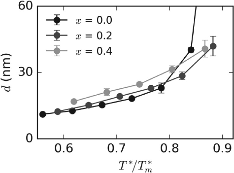
Size of 2D wurtzite and zinc-blende domains in InxGa1-xN.
Similar to our comparisons above for GaN, the InGaN-alloy layers in Figs. 8 and 9 bear similarity to thin experimental InxGa1-xN layers (x = 0.065, 0.33, 0.35, and 0.45) grown directly on sapphire by OMVPE.37 Both our simulations and these experiments yield highly faulted materials where the stacking faults again separate finely interspersed lamella comprising zb and wz phases. The measured lamella thicknesses for each phase are reported to be ∼3.5 to 5.5 nm,37 which resembles the ∼1 to 5 nm thick domains seen in Fig. 8.
B. Surface roughness and voids
Surface roughness is also analyzed for In0.4Ga0.6 N films, and the results obtained at three different temperatures of T* = 2000 K (T*/Tm* = 0.62), 2400 K (T*/Tm* = 0.74), and 2800 K (T*/Tm* = 0.87) are shown, respectively, in Figs. 11(a)–11(c). The trends of the results obtained for the In0.4Ga0.6N films in Fig. 11 are similar to those obtained for the GaN films shown in Fig. 4. Specifically, under the kinetically constrained, low-temperature conditions (i.e., T*/Tm*< 0.7), significant surface roughness and voids develop, coinciding with the presence of distinctly columnar film structure. Moreover, increasing the growth temperature is again seen to cause the surface roughness to continuously decrease, consistent with an increase in column diameter and film density. These observations further indicate that kinetically constrained conditions may also contribute to defect formation in heteroepitaxially grown InxGa1-xN films.
FIG. 11.

Surface morphology of In0.4Ga0.6 N/GaN films at (a) 2000 K (T*/Tm* = 0.62), (b) 2400 K (T*/Tm*= 0.74), and (c) 2800 K (T*/Tm* = 0.87).
RMS surface roughness is calculated at different temperatures and indium contents, and the results are shown in Fig. 12. As expected, Fig. 12 indicates that surface roughness decreases with increasing temperature. Furthermore, in the low-temperature range, surface roughness obtained at high indium content is lower than that at a low indium content given the same homologous temperature. Interestingly, in the high temperature range, surface roughness vs. homologous temperature relations obtained at different indium contents collapse to a single curve to within error. This suggests that, while low temperature diffusion kinetics may vary with indium concentration, at high temperatures, the systems begin to behave more similarly.
FIG. 12.
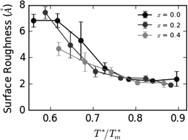
RMS surface roughness of InxGa1-xN films.
Depending on the growth conditions, InxGa1-xN alloys experimentally grown on (0001) GaN tend to roughen with increasing thickness. A variety of layers in the 3–100 nm thickness range, with compositions near x = 0.15–0.25, exhibit rough, circular mounds or islands qualitatively similar to those seen in Fig. 11.52–55 In these experiments, the measured range of island heights (∼1 to 15 nm) and widths (∼10 to 200 nm) approach those seen by MD in Figs. 11 and 12. Direct comparisons should be made with caution, however, given the wide variations in growth conditions and methods (MD vs. MBE vs. OMVPE), and also because high screw-type threading-dislocation densities in typical GaN templates yield a spiral growth mode that competes with the underlying kinetically driven roughening.52
C. Dislocation analysis
An analysis of dislocations similar to that shown in Figs. 5 and 6 is also performed for the In0.4Ga0.6 N films, and the results are shown in Figs. 13 and 14, respectively, for the two growth temperatures of 2000 K (T*/Tm* = 0.62) and 2800 K (T*/Tm* = 0.87). Again, Figs. 13(a) and 14(a) are 3D visualization of dislocation networks, Figs. 13(b) and 14(b) are plan views of dislocations in the bulk of the slab, and Figs. 13(c) and 14(c) are plan views of dislocations in the slab near the interface. It can be seen from Figs. 13(a) and 14(a) that significant dislocation densities develop during the simulated In0.4Ga0.6 N growth. On the other hand, comparisons between the dislocation plan views shown in Figs. 13 and 14 and the atomic structure plan views shown in Figs. 9 and 11 indicate that dislocations primarily occur at the boundaries of domains, consistent with the observations from GaN films discussed in Sec. III.
FIG. 13.

Visualization of dislocation networks in an In0.4Ga0.6 N film deposited at 2000 K (T*/Tm* = 0.62) showing (a) a perspective overview, (b) a slice within the bulk of the film, and (c) a slice at the film/substrate interface. Location of cross-sections (b) and (c) are indicated in (a) by the dashed planes.
FIG. 14.

Visualization of dislocation networks in an In0.4Ga0.6N film deposited at 2800 K (T*/Tm 0.87) showing (a) a perspective overview, (b) a slice within the bulk of the film, and (c) a slice at the film/substrate interface. Location of cross-sections (b) and (c) are indicated in (a) by the dashed planes.
To further quantify the observations in Figs. 13 and 14, dislocation densities are calculated as functions of temperature and location along thickness, and the results are shown in Fig. 15. It can be seen that, unlike the GaN films shown in Fig. 7, dislocation densities in InxGa1-xN films have a much more pronounced peak near the interface. This is consistent with the formation of misfit dislocations, which relieve most of the misfit strain when located near the interface. After reaching a peak near the heterointerface, dislocation densities in InxGa1-xN films continuously decay towards the surface, consistent with GaN films.
FIG. 15.

Dislocation densities in heteroepitaxial In0.4Ga0.6N films as a function of the depth position, y, within film for various homologous temperatures, T*/Tm*.
To further reveal the effects of indium on film structure, total dislocation densities are shown in Fig. 16 as a function of temperature at different indium contents. Clearly, increasing indium content increases total dislocation density. However, it should be recognized that the dislocation densities discussed here pertain to the total dislocation networks, which include both misfit dislocations and more numerous dislocations associated with domain boundaries and stacking faults. Nonetheless, the prediction of higher dislocation density at higher indium content is consistent with experimental observations. In Sec. IV D, we specifically examine misfit dislocations.
FIG. 16.
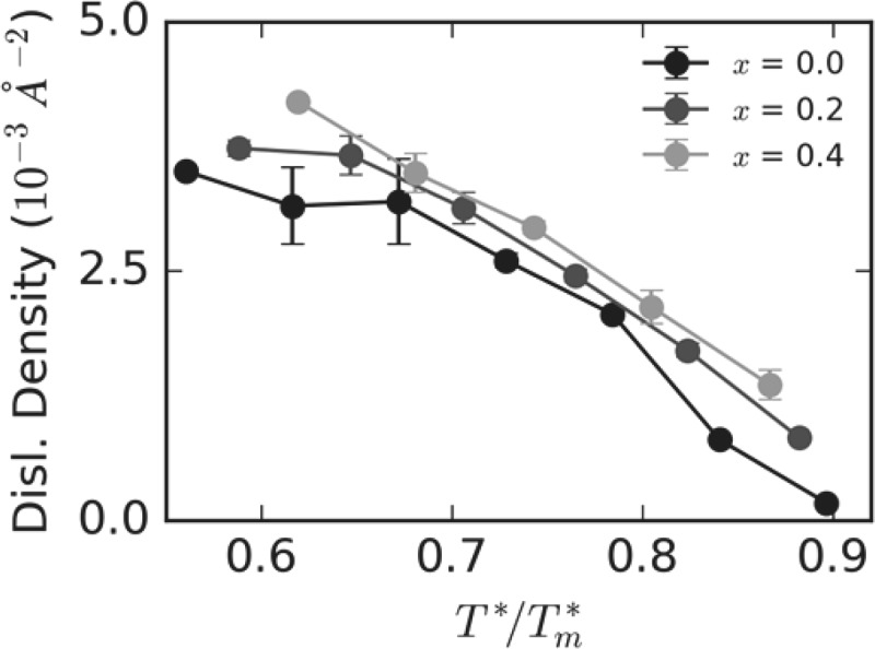
Total dislocation density in InxGa1-xN films as a function of temperature.
D. Misfit-dislocation observations
One significant concern for the growth of lattice-mismatched InxGa1-xN films on GaN substrates is the formation of misfit dislocations. Due to the complexity of the polymorphism-induced dislocation networks seen herein, a full analytical identification of misfit dislocations is currently not possible. However, by visualizing selected local slabs, excised from the MD-grown film in a way similar to experimental high-resolution microscopic analysis, misfit dislocation configurations and densities can be estimated. Using this approach, cross-sectional views of the films using thin x-y slabs are shown in Figs. 17(a)–17(c), respectively, for a homoepitaxial GaN film grown at T* = 3000 K (T*/Tm*= 0.84), for a heteroepitaxial In0.3Ga0.7 N film grown at T* = 3000 K (T*/Tm* = 0.90), and for the same heteroepitaxial In0.3Ga0.7 N film grown at a lower temperature of T* = 2800 K (T*/Tm* = 0.84).
FIG. 17.

Misfit dislocations in InxGa1-xN/GaN films at (a) x = 0.0, T* = 3000 K (T*/Tm* = 0.84); (b) x = 0.3, T* = 3000 K (T*/Tm* = 0.90); and (c) x = 0.3, T* = 2800 (T*/Tm* = 0.84). Atoms are colored by species.
It can be seen from Fig. 17(a) that along the x- direction, there are 144 planes in the substrate at the bottom, whereas there are only 143 such planes on the top surface. The one missing plane can be identified as a single edge-type dislocation located at the x-y position marked by the pair of vertical lines. This type of edge dislocations can release misfit strain in lattice-mismatched systems and hence can be considered as misfit dislocations. A similar analysis applied to Fig. 17(b) finds four misfit dislocations near the heterointerface. Using the same approach, a large number of edge type dislocations are found in Fig. 17(c). In particular, there are 12 dislocations. Interestingly, two of the dislocations create horizontal extra half planes. This is counterintuitive; nevertheless, an extra plane inside a bulk semiconductor compound has also been observed in experiments.82 For the remaining 10 dislocations, 7 of them create extra half planes below the dislocation core, and three of them create extra half planes above the dislocation core. Overall, these 10 dislocations create four missing planes on the surface, as compared to the heterointerface at the substrate boundary. Hence, the net effect of these 10 dislocations is to create four misfit dislocations, which is exactly the case in Fig. 17(b).
Based on the analysis above, Fig. 17(a) correctly indicates that for the homoepitaxial GaN/GaN films, the probability of forming edge type dislocations is very low. Fig. 17(b), on the other hand, indicates that for the lattice mismatched In0.3Ga0.7 N films, the misfit dislocation density is very high (4 misfit dislocations over a distance of approximately 23 nm). This result is qualitatively consistent with experimental observations where misfit-dislocation arrays have been observed by plan-view TEM at the In0.1Ga0.9 N/GaN heterointerface of 100 nm thick layers.48 According to calculations by Holec et al.,50 the thermodynamic critical thickness for misfit-dislocation introduction at the composition of x = 0.3 used in the simulations is only ≈ 1.6 nm. Because the simulated film thickness (15 nm) is nearly 10× the critical thickness, the observed misfit dislocations are to be expected (unless kinetically barred by the high MD growth rate). Fig. 17(c) shows that reducing temperature further increases dislocation density of the In0.3Ga0.7N films. Some of the increased dislocations, however, create the anomalous extra half planes that further increase the InGaN/GaN lattice mismatch strain. These anomalous dislocations are caused by the kinetic trapping effects and do not reflect the equilibrium misfit-dislocation density.
V. DISCUSSION
One primary observation of the present work is the formation of extensive polymorphisms during (0001) growth that are at least qualitatively comparable to the experimental observations and have a deleterious effect on the performance of SSL devices. The fundamental mechanism is a result of the fact that (0001) planes can have either ABCABC… stacking that results in a zb crystal or ABAB… stacking that results in a wz crystal. Consequently, growth on the non-polar planes of GaN, where ABAB… stacking is revealed at the growth surface, should effectively eliminate the polymorphism. As a demonstration of the use of MD to validate this hypothesis, we performed an MD simulation of growth of a homoepitaxial GaN film on a GaN substrate surface at a temperature of T* = 2800 K and a growth rate around 0.4 nm/ns. The initial substrate contains 84(100) planes in the x- direction, 12 planes in the y- direction, and 41(0001) planes in the z- direction. The final configuration obtained after 40 ns of simulated growth is shown in Fig. 18, using the same structure color scheme as in the previous figures. Figure 18 confirms that the film grown on contains a single phase of wurtzite. Thus, the MD simulation confirms that the polymorphism and the associated defects can be greatly reduced by using a non-polar growth direction. More importantly, we can see how simulated growth can provide a model for actual growth experiments. Systematic MD studies for InGaN alloys grown on surfaces are currently underway.
FIG. 18.

Simulated as-deposited GaN film grown on a GaN surface at an MD temperature of 2800 K (T*/Tm* = 0.78).
VI. CONCLUSION
The large-scale molecular dynamics simulations of InxGa1-xN growth on (0001) GaN reveal the formation of a variety of defects. Although the prediction of the highly polytypic structures might be the consequence of the approximation of Stillinger-Weber potentials (especially when combined with the high growth rates and temperatures inherent to present-day MD simulations of growth), the observed trends of temperature and indium content effects on polytypism, dislocations, voids, surface roughness, and domain-boundary structures tend to resemble known experimental observations in InGaN/GaN. Furthermore, preliminary simulations confirm that the polymorphism can be reduced by growth on non-polar surfaces such as , potentially allowing improved studies of misfit dislocation formation and strain relaxation during InGaN/GaN heteroepitaxy.
Finally, these emergent simulations of InGaN alloy growth suggest that MD-based models, combined with our development of improved SW potentials for the In:Ga:N system, offer new possibilities for exploring the atomistic mechanisms leading to defect formation during the growth of InGaN/GaN heterostructures. Based on these encouraging results, we are seeking further improvements in our MD-based methods for simulating III-nitride crystal growth. Using these methods, we are also pursuing MD studies of defect reduction in InGaN/GaN through the use of nanostructured heteroepitaxy.
ACKNOWLEDGMENTS
The Sandia National Laboratories is a multi-mission laboratory managed and operated by Sandia Corporation, a wholly owned subsidiary of Lockheed Martin Corporation, for the U.S. Department of Energy's National Nuclear Security Administration under Contract No. DE-AC04-94AL85000.
APPENDIX A: LATTICE CONSTANT
We calculated the lattice constants, a and c, for wurtzite InxGa1-xN crystals as a function of temperature T and composition x. The crystals used for the calculations contain 20 × 6(0001) × 12 planes, which is about 30 × 30 × 30 Å. The systems are equilibrated for 6 ns under the periodic boundary conditions and a zero pressure NPT (constant number of atoms, pressure, and temperature) Nosè-Hoover70,83,84 thermostat/barostat. After the first 1 ns is discarded to allow equilibration, time averaged system dimensions for the final 5 ns are used to calculate the finite temperature lattice constants. A matrix of 25 simulations consisting of 5 indium contents (x = 0.0, 0.1, 0.2, 0.3, and 0.4) and 5 temperatures (T* = 1800 K, 2200 K, 2600 K, 3000 K, and 3400 K) are performed. The MD data are fitted to the following equations (note that they should be only used for x between 0 and 0.4):
| (A1) |
| (A2) |
where a1800,GaN = 3.202 Å and c1800,GaN = 5.230 Å are lattice constants for GaN at 1800 K. Both MD data and fitted curves are shown in Figure 19. It can be seen that the fitted equations match the MD data extremely well.
FIG. 19.

Lattice constants a and c as a function of temperature T* and In content xIn ( = x): (a) a and (b) c.
Eqs. (A1) and (A2) indicate that the thermal expansion coefficients of InxGa1-xN are αa = 6.208 × 10⁻⁶ K−1 in the a-direction and αc = 5.390 × 10⁻⁶ K−1 in the c-direction and are independent on the indium content or temperature within the ranges tested. These values are close to those obtained experimentally at high temperatures.85 The lattice constants also linearly increase with indium content, nicely matching Vegard's law. At the 1800 K endpoint, Eqs. (A1) and (A2) give aGaN = 3.202 Å and cGaN = 5.230 Å, also close to experimental values at the equivalent homologous temperature defined in Appendix B.85
APPENDIX B: MELTING TEMPERATURE
Material structures depend mainly on the homologous temperature T/Tm in experiments.86 When MD melting temperature Tm* differs from the experimental melting temperature Tm, it is preferred to relate the results in terms of the homologous temperature concept T*/Tm*. To apply this concept, Tm* of InxGa1-xN is calculated as a function of indium content x.
The wz InxGa1-xN crystals used for the calculations contain 20 × 32(0001) × 12 planes, which is about 30 × 165 × 30 Å3. Following the same approach applied previously,64,87 a mixture of crystal and liquid is brought into equilibrium under the constant pressure-enthalpy (NPH) ensemble.70,83,84 After discarding the first 8 ns of simulation under the mixture state, the melting temperature is calculated as the time-averaged temperature in the next 8 ns period. This approach results in extremely small errors of less than 3 K.64 We have performed calculations for 5 indium contents (x = 0.0, 0.1, 0.2, 0.3, 0.4). The results are fitted to the following equation:
| (B1) |
where T*m,GaN = 3570 K and T*m,InN = 2715 K are respectively melting temperatures of GaN and InN. Both MD data and the fitted curve are shown in Fig. 20. It can be seen that the fitted equation matches the MD data extremely well. Interestingly, the calculated melting temperature is seen to linearly decrease with indium content.
FIG. 20.
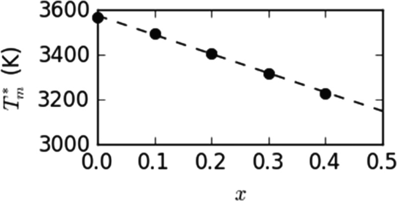
Melting temperature T* as a function of indium content x.
Note that the experimental melting temperatures for GaN and InN are respectively Tm,GaN = 2493 K (Ref. 71) and Tm,InN = 1373 K.72 As a result, our potential substantially overestimates melting temperature. In this regard, it is the predicted trends at equivalent homologous temperatures that are most informative of experiments.
References
- 1. Schubert E. F., Kim J. K., Luo H., and Xi J. Q., Rep. Prog. Phys. 69, 3069 (2006). 10.1088/0034-4885/69/12/R01 [DOI] [Google Scholar]
- 2. Shur M. S. and Zukauskas A., Proc. IEEE 93, 1691 (2005). 10.1109/JPROC.2005.853537 [DOI] [Google Scholar]
- 3. Bergh A., Craford G., Duggal A., and Haitz R., Phys. Today 54(12), 42 (2001). 10.1063/1.1445547 [DOI] [Google Scholar]
- 4. Tsao J. Y., IEEE Circuits Devices Mag. 20, 28 (2004). 10.1109/MCD.2004.1304539 [DOI] [Google Scholar]
- 5. Steigerwald D. A., Bhat J. C., Collins D., Fletcher R. M., Holcomb M. O., Ludowise M. J., Martin P. S., and Rudaz S. L., IEEE J. Sel. Top. Quantum Electron. 8, 310 (2002). 10.1109/2944.999186 [DOI] [Google Scholar]
- 6. Krames M. R., Shchekin O. B., Mueller-Mach R., Mueller G. O., Zhou L., Harbers G., and Craford M. G., J. Disp. Technol. 3, 160 (2007). 10.1109/JDT.2007.895339 [DOI] [Google Scholar]
- 7. Wu J., J. Appl. Phys. 106, 011101 (2009). 10.1063/1.3155798 [DOI] [Google Scholar]
- 8. Phillips J. M., Coltrin M. E., Crawford M. H., Fischer A. J., Krames M. R., Muller-Mach R., Mueller G. O., Ohno Y., Rohwer L. E. S., Simmons J. A., and Tsao J. Y., Laser Photonics Rev. 1, 307 (2007). 10.1002/lpor.200710019 [DOI] [Google Scholar]
- 9. Feng W., Kuryatkov V. V., Chandolu A., Song D. Y., Pandikunta M., Nikishin S. A., and Holtz M., J. Appl. Phys. 104, 103530 (2008). 10.1063/1.3029695 [DOI] [Google Scholar]
- 10. Zhao H. P., Liu G. Y., Li X. H., Arif R. A., Huang G. S., Poplawsky J. D., Penn S. T., Dierolf V., and Tansu N., IET Optoelectron. 3, 283 (2009). 10.1049/iet-opt.2009.0050 [DOI] [Google Scholar]
- 11. Zhao H. P., Liu G. Y., Zhang J., Poplawsky J. D., Dierolf V., and Tansu N., Opt. Express A 19, 991 (2011). 10.1364/OE.19.00A991 [DOI] [PubMed] [Google Scholar]
- 12. Liliental-Weber Z., Benamara M., Washburn J., Domagala J. Z., Bak-Misiuk J., Piner E. L., Roberts J. C., and Bedair S. M., J. Electron. Mater. 30, 439 (2001). 10.1007/s11664-001-0056-5 [DOI] [Google Scholar]
- 13. Song T. L., J. Appl. Phys. 98, 084906 (2005). 10.1063/1.2108148 [DOI] [Google Scholar]
- 14. Lu W., Li D. B., Li C. R., and Zhang Z., J. Appl. Phys. 96, 5267 (2004). 10.1063/1.1803633 [DOI] [Google Scholar]
- 15. Pereira S., Thin Solid Films 515, 164 (2006). 10.1016/j.tsf.2005.12.144 [DOI] [Google Scholar]
- 16. Li Q. and Wang G. T., Appl. Phys. Lett. 97, 181107 (2010). 10.1063/1.3513345 [DOI] [Google Scholar]
- 17. J. J. Wierer, Jr. , Li Q., Koleske D. D., Lee S. R., and Wang G. T., Nanotechnology 23, 194007 (2012). 10.1088/0957-4484/23/19/194007 [DOI] [PubMed] [Google Scholar]
- 18. Li Y., You S., Zhu M., Zhao L., Hou W., Detchprohm T., Taniguchi Y., Tamura N., Tanaka S., and Wetzel C., Appl. Phys. Lett. 98, 151102 (2011). 10.1063/1.3579255 [DOI] [Google Scholar]
- 19. Ee Y. K., Biser J. M., Cao W., Chan H. M., Vinci R. P., and Tansu N., IEEE J. Sel. Top. Quantum Electron. 15, 1066 (2009). 10.1109/JSTQE.2009.2017208 [DOI] [Google Scholar]
- 20. Kuykendall T., Ulrich P., Aloni S., and Yang P., Nat. Mater. 6, 951 (2007). 10.1038/nmat2037 [DOI] [PubMed] [Google Scholar]
- 21. Inaba Y., Onozu T., Takami S., Kubo M., Miyamoto A., and Imamura A., Jpn. J. Appl. Phys. 40, 2991 (2001). 10.1143/JJAP.40.2991 [DOI] [Google Scholar]
- 22. Lei H. P., Chen J., Petit S., Ruterana P., Jiang X. Y., and Nouet G., SuperLattices Microstruct. 40, 464 (2006). 10.1016/j.spmi.2006.09.010 [DOI] [Google Scholar]
- 23. Zhang Z., Chatterjee A., Grein C., Ciani A., and Chung P. W., J. Vac. Sci. Techol., B 29, 03C133 (2011). 10.1116/1.3579462 [DOI] [Google Scholar]
- 24. Onozu T., Miura R., Takami S., Kubo M., Miyamoto A., Iyechika Y., and Maeda T., Jpn. J. Appl. Phys. 39, 4400 (2000). 10.1143/JJAP.39.4400 [DOI] [Google Scholar]
- 25. Zhou X. W., Murdick D. A., Gillespie B., and Wadley H. N. G., Phys. Rev. B 73, 045337 (2006). 10.1103/PhysRevB.73.045337 [DOI] [Google Scholar]
- 26. Chen Z., Yu Z., Lu P., and Liu Y., Physica B 404, 4211 (2009). 10.1016/j.physb.2009.07.193 [DOI] [Google Scholar]
- 27. Kobayashi Y., Doi Y., and Nakatani A., Jpn. J. Appl. Phys. 49, 115601 (2010). 10.1143/JJAP.49.115601 [DOI] [Google Scholar]
- 28. Gong X., Xu K., Wang J., Yang H., Bian L., Zhang J., and Xu Z., Physica B 406, 36 (2011). 10.1016/j.physb.2010.10.007 [DOI] [Google Scholar]
- 29. Kawamura T., Kangawa Y., Kakimoto K., Kotake S., and Suzuki Y., Jpn. J. Appl. Phys. 51, 01AF06 (2012). 10.7567/JJAP.51.01AF06 [DOI] [Google Scholar]
- 30. Zhou A., Xiu X.-Q., Zhang R., Xie Z.-L., Hua X.-M., Lui B., Han P., Gu S.-L., Shi Y., and Zheng Y.-D., Chin. Phys. B 22, 017801 (2013). 10.1088/1674-1056/22/1/017801 [DOI] [Google Scholar]
- 31. Gong X., Dogan P., Zhang X., Jahn U., Xu K., Bian L., and Yang H., Jpn. J. Appl. Phys. 53, 085601 (2014). 10.7567/JJAP.53.085601 [DOI] [Google Scholar]
- 32. Kawamura T., Hayashi H., Miki T., Suzuki Y., Kangawa Y., and Kakimoto K., Jpn. J. Appl. Phys. 53, 05FL08 (2014). 10.7567/JJAP.53.05FL08 [DOI] [Google Scholar]
- 33. Wu X. H., Kapolnek D., Tarsa E. J., Heying B., Keller S., Keller B. P., Mishra U. K., DenBaars S. P., and Speck J. S., Appl. Phys. Lett. 68, 1371 (1996). 10.1063/1.116083 [DOI] [Google Scholar]
- 34. Wu X. H., Fini P., Tarsa E. J., Heying B., Keller S., Mishra U. K., Denbaars S. P., and Speck J. S., J. Cryst. Growth 189, 231 (1998). 10.1016/S0022-0248(98)00240-1 [DOI] [Google Scholar]
- 35. Kim C. C., Je J. H., Yi M. S., Noh D. Y., and Ruterana P., J. Appl. Phys. 90, 2191 (2001). 10.1063/1.1388859 [DOI] [Google Scholar]
- 36. Narayanan V., Lorenz K., Kim W., and Mahajan S., Philos. Mag. A 82, 885 (2002). 10.1080/01418610208240008 [DOI] [Google Scholar]
- 37. Cho H. K., Lee J. Y., Kim K. S., and Yang G. M., Appl. Phys. Lett. 77, 247 (2000). 10.1063/1.126939 [DOI] [Google Scholar]
- 38. Poliani E., Wagner M. R., Reparaz J. S., Mandl M., Strassburg M., Kong X., Trampert A., Torres C. M. S., Hoffmann A., and Maultzsch J., Nano Lett. 13, 3205 (2013). 10.1021/nl401277y [DOI] [PubMed] [Google Scholar]
- 39. Heying B., Wu X. H., Keller S., Li Y., Kapolnek D., Keller B. P., DenBaars S. P., and Speck J. S., Appl. Phys. Lett. 68, 643 (1996). 10.1063/1.116495 [DOI] [Google Scholar]
- 40. Belabbas I., Ruterana P., Chen J., and Nouet G., Philos. Mag. 86, 2241 (2006). 10.1080/14786430600651996 [DOI] [Google Scholar]
- 41. Levedev V., Cimalla V., Pezoldt J., Himmerlich M., Krischok S., Schaefer J. A., Ambacher O., Morales F. M., Lozano J. G., and Ganzalez D., J. Appl. Phys. 100, 094902 (2006). 10.1063/1.2363233 [DOI] [Google Scholar]
- 42. Lester S. D., Ponce F. A., Craford M. G., and Steigerwald D. A., Appl. Phys. Lett. 66, 1249 (1995). 10.1063/1.113252 [DOI] [Google Scholar]
- 43. Visconti P., Huang D., Yun F., Reshchikov M. A., King T., Cingolani R., Jasinski J., Liliental-Weber Z., and Morkoc H., Phys. Status Solidi A 190, 5 (2002). [DOI] [Google Scholar]
- 44. Cho H. K., Lee J. Y., Kim C. S., and Yang G. M., J. Electron. Mater. 30, 1348 (2001). 10.1007/s11664-001-0123-y [DOI] [Google Scholar]
- 45. Zhu M., You S., Detchprohm T., Paskova T., Preble E. A., and Wetzel C., Phys. Status Solidi A 207, 1305 (2010). 10.1002/pssa.200983645 [DOI] [Google Scholar]
- 46. Jahnen B., Albrecht M., Dorsch W., Christiansen S., Strunk H. P., Hanser D., and Davis R. F., MRS Int. J. Nitr. Semi. Res. 3, 39 (1998). [Google Scholar]
- 47. Romanov A. E., Young E. C., Wu F., Tyagi A., Gallinat C. S., Nakamura S., DenBaars S. P., and Speck J. S., J. Appl. Phys. 109, 103522 (2011). 10.1063/1.3590141 [DOI] [Google Scholar]
- 48. Srinivasan S., Geng L., Liu R., Ponce F. A., Narukawa Y., and Tanaka S., Appl. Phys. Lett. 83, 5187 (2003). 10.1063/1.1633029 [DOI] [Google Scholar]
- 49. Liu R., Mei J., Srinivasan S., Ponce F. A., Omiya H., Narukawa Y., and Mukai T., Appl. Phys. Lett. 89, 201911 (2006). 10.1063/1.2388895 [DOI] [Google Scholar]
- 50. Holec D., Costa P. M. F. J., Kappers M. J., and Humphreys C. J., J. Cryst. Growth 303, 314 (2007). 10.1016/j.jcrysgro.2006.12.054 [DOI] [Google Scholar]
- 51. Qian W., Rohrer G. S., Skowronski M., Doverspike K., Rowland L. B., and Gaskill D. K., Appl. Phys. Lett. 67, 2284 (1995). 10.1063/1.115127 [DOI] [Google Scholar]
- 52. Keller S., Mishra U. K., DenBaars S. P., and Siefert W., Jpn. J. Appl. Phys. 37, L431 (1998). 10.1143/JJAP.37.L431 [DOI] [Google Scholar]
- 53. Damilano B., Grandjean N., Vezian S., and Massies J., J. Cryst. Growth 227, 466 (2001). 10.1016/S0022-0248(01)00744-8 [DOI] [Google Scholar]
- 54. Neugebauer J., Zywietz T. K., Scheffler M., Northrup J. E., Chen H., and Feenstra R. M., Phys. Rev. Lett. 90, 056101 (2003). 10.1103/PhysRevLett.90.056101 [DOI] [PubMed] [Google Scholar]
- 55. Oliver R. A., Kappers M. J., Humphreys C. J., Andrew G., and Briggs D., J. Appl. Phys. 97, 013707 (2005). 10.1063/1.1823581 [DOI] [Google Scholar]
- 56. Heying B., Averbach R., Chen L. F., Haus E., Riechert H., and Speck J. S., J. Appl. Phys. 88, 1855 (2000). 10.1063/1.1305830 [DOI] [Google Scholar]
- 57. Adelmann C., Brault J., Jalabert D., Gentile P., Mariette H., Mula G., and Daudin B., J. Appl. Phys. 91, 9638 (2002). 10.1063/1.1471923 [DOI] [Google Scholar]
- 58. Koblmuller G., Fernandez-Garrido S., Calleja E., and Speck J. S., Appl. Phys. Lett. 91, 161904 (2007). 10.1063/1.2789691 [DOI] [Google Scholar]
- 59. Sun C. J., Anwar M. Z., Chen Q., Yang J. W., A. Khan M., Shur M. S., Bykhovski A. D., Liliental-Weber Z., Kisielowski C., Smith M., Lin J. Y., and Xiang H. X., Appl. Phys. Lett. 70, 2978 (1997). 10.1063/1.118762 [DOI] [Google Scholar]
- 60. Wu X. H., Elsass C. R., Abare A., Mack M., Keller S., Petroff P. M., DenBaars S. P., Speck J. S., and Rosner S. J., Appl. Phys. Lett. 72, 692 (1998). 10.1063/1.120844 [DOI] [Google Scholar]
- 61. Massabuau F. C.-P., Sahonta S.-L., Trinh-Xuan L., Rhode S., Puchtler T. J., Kappers M. J., Humphreys C. J., and Oliver R. A., Appl. Phys. Lett. 101, 212107 (2012). 10.1063/1.4768291 [DOI] [Google Scholar]
- 62. Zhao Y., Wu F., Huang C. Y., Kawaguchi Y., Tanaka S., Fujito K., Speck J. S., DenBaars S. P., and Nakamura S., Appl. Phys. Lett. 102, 091905 (2013). 10.1063/1.4794864 [DOI] [Google Scholar]
- 63. Yankovich A. B., Kvit A. V., Li X., Zhang F., Avrutin V., Liu H. Y., Izyumskaya N., Ozgur U., Morkoc H., and Voyles P. M., J. Appl. Phys. 111, 023517 (2012). 10.1063/1.3679540 [DOI] [Google Scholar]
- 64. Zhou X. W., Jones R. E., and Gruber J., Comput. Mater. Sci. 128, 331 (2017). 10.1016/j.commatsci.2016.11.047 [DOI] [Google Scholar]
- 65. Lei H., Chen J., Jiang X., and Nouet G., Micro. J. 40, 342 (2009). 10.1016/j.mejo.2008.07.068 [DOI] [Google Scholar]
- 66. Stillinger F. H. and Weber T. A., Phys. Rev. B 31, 5262 (1985). 10.1103/PhysRevB.31.5262 [DOI] [PubMed] [Google Scholar]
- 67. Yeh C.-Y., Lu Z. W., Froyen S., and Zunger A., Phys. Rev. B 46, 10086 (1992). 10.1103/PhysRevB.46.10086 [DOI] [PubMed] [Google Scholar]
- 68.See http://lammps.sandia.gov for Large-scale Atomic/Molecular Massively Parallel Simulator (LAMMPS).
- 69. Plimpton S., J. Comput. Phys. 117, 1 (1995). 10.1006/jcph.1995.1039 [DOI] [Google Scholar]
- 70. Hoover W. G., Phys. Rev. B 31, 1695 (1985). 10.1103/PhysRevA.31.1695 [DOI] [PubMed] [Google Scholar]
- 71. Utsumi W., Saitoh H., Kaneko H., Watanuki T., Aoki K., and Shimomura O., Nat. Mater. 2, 735 (2003). 10.1038/nmat1003 [DOI] [PubMed] [Google Scholar]
- 72. MacChesney J. B., Bridenbaugh P. M., and O'Connor P. B., Mater. Res. Bull. 5, 783 (1970). 10.1016/0025-5408(70)90028-0 [DOI] [Google Scholar]
- 73. Zhou X. W. and Wadley H. N. G., J. Appl. Phys. 84, 2301 (1998). 10.1063/1.368297 [DOI] [Google Scholar]
- 74. Zhou X. W., Wadley H. N. G., Johnson R. A., Larson D. J., Tabat N., Cerezo A., Petford-Long A. K., Smith G. D. W., Clifton P. H., Martens R. L., and Kelly T. F., Acta Mater. 49, 4005 (2001). 10.1016/S1359-6454(01)00287-7 [DOI] [Google Scholar]
- 75. Chavez J. J., Zhou X. W., Almeida S. F., Aguirre R., and Zubia D., J. Mater. Sci. Res. 5, 1 (2016). 10.5539/jmsr.v5n3p1 [DOI] [Google Scholar]
- 76. Maras E., Trushin O., Stukowski A., Ala-Nissila T., and Jonsson H., Comput. Phys. Commun. 205, 13 (2016). 10.1016/j.cpc.2016.04.001 [DOI] [Google Scholar]
- 77. Stukowski A. and Albe K., Modell. Simul. Mater. Sci. Eng. 18, 085001 (2010). 10.1088/0965-0393/18/8/085001 [DOI] [Google Scholar]
- 78. Stukowski A., Bulatov V. V., and Arsenlis A., Modell. Simul. Mater. Sci. Eng. 20, 085007 (2012). 10.1088/0965-0393/20/8/085007 [DOI] [Google Scholar]
- 79. Lee H. J., Ryu H., Lee C., and Kim K., J. Cryst. Growth 191, 621 (1998). [Google Scholar]
- 80. Selke H., Kirchner V., Heinke H., Einfeldt S., Ryder P., and Hommel D., J. Cryst. Growth 208, 57 (2000). 10.1016/S0022-0248(99)00462-5 [DOI] [Google Scholar]
- 81. Ostwald W., Zeit. Phys. Chem. 22, 289 (1897). [Google Scholar]
- 82. Li C., Poplawsky J., Wu Y., Lupini A. R., Mouti A., Leonard D. N., Paudel N., Jones K., Yin W., Al-Jassim M., Yan Y., and Pennycook S. J., Ultramicroscopy 134, 113 (2013). 10.1016/j.ultramic.2013.06.010 [DOI] [Google Scholar]
- 83. Tuckerman M. E., Alejandro J., López-Rendón R., Jochim A. L., and Martyna G. J., J. Phys. A: Math. Gen. 39, 5629 (2006). 10.1088/0305-4470/39/19/S18 [DOI] [Google Scholar]
- 84. Shinoda W., Shiga M., and Mikami M., Phys. Rev. B 69, 134103 (2004). 10.1103/PhysRevB.69.134103 [DOI] [Google Scholar]
- 85. Roder C., Einfeldt S., Figge S., and Hommel D., Phys. Rev. B 72, 085218 (2005). 10.1103/PhysRevB.72.085218 [DOI] [Google Scholar]
- 86. Thornton J. A., J. Vac. Sci. Technol. 11, 666 (1974). 10.1116/1.1312732 [DOI] [Google Scholar]
- 87. Morris J. R., Wang C. Z., Ho K. M., and Chan C. T., Phys. Rev. B 49, 3109 (1994). 10.1103/PhysRevB.49.3109 [DOI] [PubMed] [Google Scholar]