Abstract
We report on the synthesis of large-area molybdenum disulfide (MoS2) film on an insulating substrate by means of chemical vapor deposition. A single mixture of molybdenum hexacarbonyl (Mo(CO)6) and dimethyl disulfide (C2H6S2) was utilized as an organic liquid precursor for the synthesis of MoS2 film. Carbon impurities stemming from the dissociation of the organic precursor are effectively removed by water oxidation, and hydrogen gas, which is a by-product of the oxidation of carbon impurities, inhibits the formation of molybdenum oxides. The use of a liquid precursor assisted with water oxidation ensures high reproducibility and full-coverage of MoS2 film for large area, which is not typically achieved with solid precursors such as molybdenum oxide and sulfur powder. We believe that our approach will advance the synthesis of transition metal dichalcogenides.
Introduction
Two dimensional (2D) semiconducting transition metal dichalcogenides (s-TMdCs) MX2 (M = Mo or W; X = S or Se) have been highlighted due to their unique physical and chemical properties1–6. The energy band gaps of s-TMdCs vary from 1 to 2 eV, depending on their constituents. Monolayer s-TMdCs are the direct band gap semiconductors, and multilayer s-TMdCs are the indirect band gap semiconductors, so the unique properties of these materials can be tailored for specific applications7–9. For instance, monolayer s-TMdCs are very useful in optoelectronic devices due to their high photoluminescence (PL) quantum yield while multilayer s-TMdCs are more appropriate for use in high-speed thin film transistors due to their multichannel carrier path10, 11. Among s-TMdCs family, MoS2 has been extensively used as a lubricant and as an efficient catalyst for hydrogen evolution12–14. In particular, monolayer or few layer MoS2 field effect transistors (FETs) exhibit the highest carrier mobility up to 200 cm2 V−1 s−1 at room temperature due to the lower effective mass when compared to that of other s-TMdCs, and MoS2 has also been applied in flexible and transparent electronics1, 15–17. However, it is still challenging to obtain the large-area, high-quality MoS2 films.
Several methods have been suggested to obtain large-area MoS2 films, including chemical vapor deposition (CVD), atomic layer deposition (ALD), and molecular beam epitaxy (MBE)18–27. Although the thickness of MoS2 film can be controlled with high coverage via ALD, the crystallinity of MoS2 film is poor19. The possibility of synthesizing MoS2 using MBE on graphene substrate has also been proposed18. However, the MBE system is limited to industrial applications due to its high cost and low throughput. Compared to other methods, CVD has advantages in terms of its low cost, high throughput, and ability to grow large-area, high-quality MoS2 films.
Monolayer MoS2 was successfully synthesized via CVD in 2012, and since then, many researchers have investigated the use of various precursors, growth substrates, and growth parameters, including the pressure, flux of precursor, and temperature, to obtain large-area, high-quality MoS2 films22–25. Various seeding promoter to increase the adhesion between precursors and substrate has also been studied20, 21. Here, we focus on the precursors because precursors are inevitable factor to grow MoS2 films. Typically, solid-phase precursors such as molybdenum oxide and sulfur powders have been used21, 26, 27. However, it is difficult to control the vaporization of solid precursor by temperature, resulting in limitations in a consecutive and constant supply of precursors during the growth process24, 26. As a consequence, the growth results are not highly repeatable, and the thickness and coverage uniformities of MoS2 film cannot be ensured. Unlike solid-phase precursors, a gas phase precursor has an advantage in that it offers controllability28. Hydrogen sulfide can be utilized as sulfur precursor, but it is very toxic, and special care is therefore necessary28. Unfortunately, to the best of our knowledge, a gas phase precursor for molybdenum has not yet been reported. On the other hand, a liquid phase precursor is also an alternative. Metal organic chemical vapor deposition (MOCVD) with a bubbler system is widely used to grow III-nitride materials such as GaN and AlN using liquid precursors29, 30. Recently, a combination of diethyl sulfide ((C2H5)2S, liquid phase) and molybdenum hexacarbonyl (Mo(CO)6, solid phase) was used to grow a monolayer MoS2 film31. However, the growth time for the complete monolayer MoS2 film took around a day, so it is still necessary to investigate new types of precursors.
Herein, we report on the use of a single organic liquid precursor in the synthesis of large-area MoS2 film. The single liquid precursor is prepared by the dissolution of molybdenum hexacarbonyl in dimethyl disulfide ((CH3)2S2). The coverage of MoS2 film is controlled by adjusting the growth time, resulting in the formation of full-coverage MoS2 films within 15 minutes. Carbon impurities stemming from the dissociation of organic precursors are effectively removed by water oxidation, as confirmed via Raman spectroscopy and photoluminescence (PL) measurements. Furthermore, the detailed growth mechanism is discussed.
Results and Discussion
The bubbler system was equipped in CVD as shown in Fig. 1(a), to synthesize the MoS2 film. 0.04 M of Mo(CO)6 powder was dissolved in (CH3)2S2, and the precursor solution was further analyzed via liquid chromatography-mass spectrometry (see Figure S1 in Supplementary Information). The presence of Mo and S chemicals was confirmed as Mo ions, C2H8OS, Mo(CO)2, Mo(CO)5, C5HMoO6, and C6HMoO7. Unfortunately, dimethyl disulfide was not detected due to the detection limit, but we assume that dimethyl disulfide should also be present in the precursor solution. To remove the carbon impurities, a separate water bubbler is installed. Argon is used as a carrier, and the adhesion between the precursor and the SiO2/Si substrate is increased by coating perylene-3,4,9,10-tetracarboxylic acid tetrapotassium salt (PTAS) on the SiO2/Si substrate20. Figure 1(b) shows photographs of bare SiO2/Si, as-grown MoS2 film, and transferred MoS2 film on SiO2/Si substrate. The color of SiO2/Si substrate changed violet to blue-green after growth. Furthermore, the MoS2 film was transferred on the SiO2/Si substrate using the conventional poly(methyl methacrylate) (PMMA) method, and it exhibit similar color as that of as-grown MoS2 film, indicating that the MoS2 film was well transferred on the target substrate. Figure 1(c) shows AFM image of the transferred MoS2 film. The characteristic wrinkles of MoS2 are clearly visible. The inset in Fig. 1(c) shows the height profile along the white-dotted line in Fig. 1(c), and the thickness of MoS2 film is of around 0.85 nm, which is similar to the thickness of monolayer (ML) MoS2 (0.615 nm)32. It is worth noting that WS2 was successfully synthesized using another single liquid precursor that had been prepared by the dissolving of W(CO)6 in (CH3) 2S2, instead of Mo(CO)6 (see Figure S2 in Supplementary Information).
Figure 1.
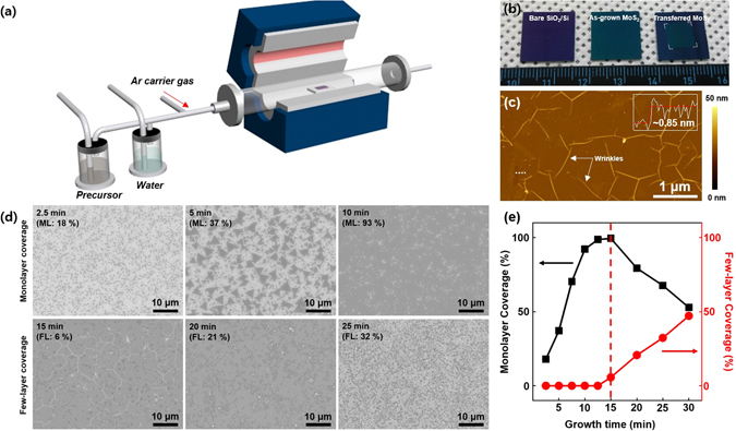
Synthesis of MoS2 film. (a) Schematic illustration of the CVD system with a liquid precursor and water bubblers. The bubblers are connected with individual mass flow controllers. (b) Photographs of the bare SiO2/Si substrate, as-grown MoS2 film, and transferred MoS2 film. (c) Atomic force microscopy image of the transferred MoS2 film. The inset indicates the height profile along the dotted white line. The white arrows present the MoS2 wrinkles. (d) SEM images of as-grown MoS2 as a function of the growth time. The dark region indicates MoS2, and the white background indicates the SiO2/Si substrate. The coverage for monolayer (ML) and few-layer (FL) MoS2 is displayed in each SEM image. (e) The coverage for monolayer (black) and few-layer (red) MoS2 regions as a function of the growth time.
A time evolution experiment was carried out to understand the growth behavior. Figure 1(d) shows scanning electron microscopy (SEM) images of as-grown MoS2 for 2.5, 5, 10, 15, 20, and 25 min, respectively. For 2.5 min growth, small ML MoS2 flakes were grown. Within 10 min, the area coverage of ML MoS2 increased up to 93%. After 15 min growth, the coverage of ML MoS2 is almost 94% with 6% few-layer (FL) MoS2. With a more prolonged growth time of 25 min, the portion of the FL MoS2 increased. Figure 1(e) displays the ML and FL coverage as a function of the growth time. The coverage of the ML MoS2 reached ~100% within 15 min and then gradually decreased with the growth time. On the other hand, the coverage of FL MoS2 increased from 15 min growth and reached almost 50% at 30 min of growth. This implies that ML MoS2 starts to grow at the initial stage as a bottom layer followed by the growth of FL MoS2 on top of monolayer MoS2, which is similar to the growth behavior of hexagonal boron nitride on Cu foils33.
It is expected that carbon impurities will be present on the growth substrate since the precursor contains carbon. Therefore, the presence of carbon was confirmed via Raman spectroscopy. Figure 2(a,b) show the Raman spectra of MoS2 for different growth conditions: without water, with 1 sccm water, and with 10 sccm water. The peaks of E1 2g (382 cm−1) and A1g (404 cm−1) originated from in-plane and out-of-plane phonon vibrations, respectively, are clearly seen for the sample grown without water supply (Fig. 2(a)). As expected, the peaks of the defect-related D-band near 1330 cm−1 and the graphite related G-band near 1580 cm−1 are detected in the Raman spectra, indicating that carbon impurities exist. We further confirmed the presence of amorphous carbon (a-C) on whole regions of the growth substrate via Raman mapping technique (see Figure S3 in Supplementary Information). Previous work showed that the a-C can be effectively eliminated with water, realizing the super growth of carbon nanotube forest34. Therefore, the water was introduced in this work as a weak oxidizer. The carbon atoms are eliminated by the following chemical reaction34.
| 1 |
Figure 2.
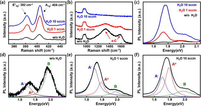
Effect of water supply I: the removal of a-C. (a,b) Raman and (c) PL spectra of MoS2 specimens with/without water supply (black: without (w/o) water, red: H2O 1 sccm, and blue: H2O 10 sccm, respectively). Each Raman spectrum for (a) and (b) display the presence of MoS2 and a-C, respectively. (d,e) Deconvoluted PL spectra of (d) w/o water, (e) H2O 1 sccm, and (f) H2O 10 sccm water with Lorentzian curves at 1.852 eV (blue, multiexciton, A−), 1.895 eV (red, neutral exciton, A°), and 1.988 eV (green, neutral exciton, B), respectively.
It is reported that the Gibbs free energy of Reaction 1 is changes from plus to minus at ~670 °C. This indicates that for Reaction 1 to be spontaneous, a minimum temperature of ~670 °C is required35. At 650 °C growth, the carbon impurities were not effectively removed (see Figure S4 in Supplementary Information). Reaction 1 shows that carbon monoxide and hydrogen molecule are evolved. With 1 sccm of water, the peaks of the D-band and G-band slightly decreased (Fig. 2(b)) whereas the peak intensities for E1 2g and A1g increased (Fig. 2(a)). Eventually, the a-C is completely removed when 10 sccm water supply is used. We further confirmed the entire removal of a-C via Raman mapping (see Figure S5 in Supplementary Information). Typically, ML MoS2 exhibits a strong PL intensity due to the direct band transition nature7. Figure 2(c) shows the PL spectra of MoS2 with/without the water supply. While the PL intensity is very weak without a water supply, it gradually increases as a function of the flow rate of water. To clarify the change in the PL intensity, each PL spectrum was fitted with a Lorentzian curve, as shown in Fig. 2(d–f). In the absence of water, the intensity of the neutral exciton (A°) peak near 1.895 eV is very weak, whereas multiexciton (A−) near 1.852 eV and neutral exciton (B) near 1.988 eV are observed to be stronger36. However, those peaks are not strong when compared to those of water supply. As the water supply increases, the intensity of the A° exciton peak becomes more intense compared to those of other peaks, indicating that the overall PL intensity has increased. The change of PL intensity, such as PL quenching without water supply and the increase of A° exciton intensity with water supply might be related to the presence of a-C and molybdenum oxide. In the presence of a-C, the excited electron might be transferred to the conduction band of the conductive a-C, leading to PL quenching37. On the other hand, in the absence of a-C, a strong PL intensity is clearly observed. The presence of molybdenum oxides will be discussed later on, but the increase of the neutral exciton A° with the water supply might also be attributed to the undoping effect on MoS2 by the removal of the molybdenum oxide38–40. As a consequence, a-C is effectively removed via water oxidation. It is noted that the water supply promotes the generation of radicals by hydrolysis and hydrogenolysis reactions of precursors, expecting that small MoS2 flakes are grown31. Even though the flux of radicals increases in the presence of water, the amount of radicals which participate in the growth of MoS2 at high temperature decreases due to the higher desorption rate41. Therefore, a fair quality of MoS2 film within ~15 min is achieved.
Regarding the molybdenum oxide, we found unresolved particles from SEM and AFM images in the sample surface when water was not supplied, as shown in Fig. 3(a,b). Furthermore, it should be emphasized that full-coverage MoS2 film was not achieved even with growth time exceeding 2 hours with the presence of several particles. To elucidate the chemical composition of those particles, the samples were further analyzed via X-ray photoelectron microscopy (XPS) and transmission electron microscopy (TEM). Figure 3(c,d) show the XPS spectra of Mo 3d and S 2p core levels with/without water supply. Typically, bulk MoS2 shows three characteristic peaks for Mo4+3d3/2 (~232 eV), Mo4+3d5/2 (~229 eV), and S 2s (~226.13 eV) in the Mo 3d core level spectra and two peaks for S 2p1/2 and S 2p3/2 in the S 2p core level spectra42. Meanwhile the XPS spectra for the S 2p core level is similar regardless of the water supply, and the Mo 3d core level spectra changed due to the presence of water. When water was not supplied, four distinct peaks could be observed, and one peak near 235.2 eV disappeared gradually as the water supply increased (Fig. 3(c)). Gaussian curve fitting was used to assign the additional peaks in Mo 3d core level spectra to the Mo6+3d3/2 and Mo6+3d5/2 of molybdenum oxide43. It is not currently clear why molybdenum oxide formed, but those were eliminated when water was supplied. Hydrogen gases released in Reaction 1, reduces the molybdenum oxide as shown in Reaction 2, resulting in the generation of the molybdenum suboxide and water44.
| 2 |
| 3 |
Figure 3.
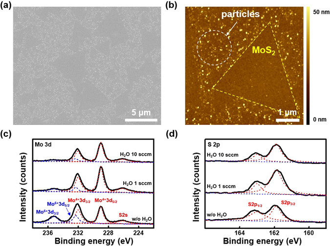
Effect of water supply II: removal of molybdenum oxides. (a) SEM, (b) AFM images of as-grown MoS2 flakes without the water supply. Unresolved particles are distributed on the whole region. (c,d) XPS core level spectra of (c) Mo 3d and (d) S 2p for three MoS2 specimens: without (w/o) water, H2O 1 sccm, and H2O 10 sccm, respectively. The characteristic peaks of Mo4+3d3/2, Mo4+3d5/2, S 2s, S 2p1/2, and S 2p3/2 correspond to MoS2 whereas the peaks of Mo6+3d3/2 and Mo6+3d5/2 correspond to molybdenum oxide.
The generated suboxide participates in the formation of MoS2 via Reaction 3 20. The removal of molybdenum oxide was further confirmed via TEM analysis. Figure 4 shows TEM images of MoS2 with/without water supply. Without water supply, molybdenum oxide particles are observed on the MoS2 film (Fig. 4(a,b)). In Fig. 4(b), the inset shows the fast Fourier transformation (FFT) of the white-dashed box. The parallelogram-shaped dots are assigned to the (131), (−111), (004), and (034) planes of MoO3, according to a previous reports45, 46. Figure 4(c) shows a high resolution TEM image of molybdenum oxide particles, and the parallelogram-shaped lattice structure is clearly identified. The value for d-spacing for the (−111) and (131) planes were obtained as 0.263 and 0.255 nm, which is in good agreement with the previous results obtained for molybdenum trioxide (MoO3)45, 46. Therefore, the particle is deduced to be MoO3 with an orthorhombic structure. With the water supply, such particles were not observed on the MoS2 film, as shown in Fig. 4(d,e). The hexagonal-shaped FFT pattern in the inset of Fig. 4(e) is obtained from the white-dashed box in Fig. 4(e). The hexagonal dots are assigned to the (10–10) and (11–20) planes of MoS2, according to a previous report47. The high-resolution TEM image in Fig. 4(f) shows the apparently hexagonal structure of MoS2. The d-spacings for the (10–10) and (11–20) planes are 0.27 nm and 0.16 nm, respectively. Those values match well with previously reported values20, indicating that the MoS2 film has been successfully synthesized.
Figure 4.
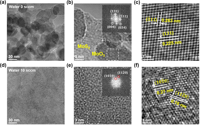
TEM analyses of unresolved particles and MoS2. (a–f) TEM images of MoS2 at different magnifications (a–c) with and (d–f) without water supply. The insets of (b) and (e) indicate the fast Fourier transform (FFT) patterns in the white-dashed box for each image. (c,f) Zoomed-in TEM images of white-dashed boxes in (b) and (e), respectively.
Figure 5 illustrates the growth mechanism for MoS2 with/without water supply. In the absence of water, various kinds of molybdenum oxides and a-Cs are easily deposited on the growth substrate during growth, resulting in the formation of MoO3 particles and a-Cs. These unwanted impurities limit the evolution of continuous the MoS2 film (Fig. 5(a)). In contrast, the water supply during growth can lead to effective removal of a-C via Reaction 1. In addition, the hydrogen gases stemming from Reaction 1 plays an important role in removing the impurities and enhancing the lateral growth of the MoS2. Firstly, molybdenum oxide is reduced to molybdenum suboxide by the hydrogen, releasing water and carbon monoxide via Reaction 1. Secondly, the reduced molybdenum suboxides participate in the lateral growth of the MoS2 film via Reaction 3, resulting in full coverage of the MoS2 film without any other impurities (Fig. 5(b)). As a consequence, MoS2 films can be synthesized with water oxidation of a-C and reduction of molybdenum oxide impurities.
Figure 5.
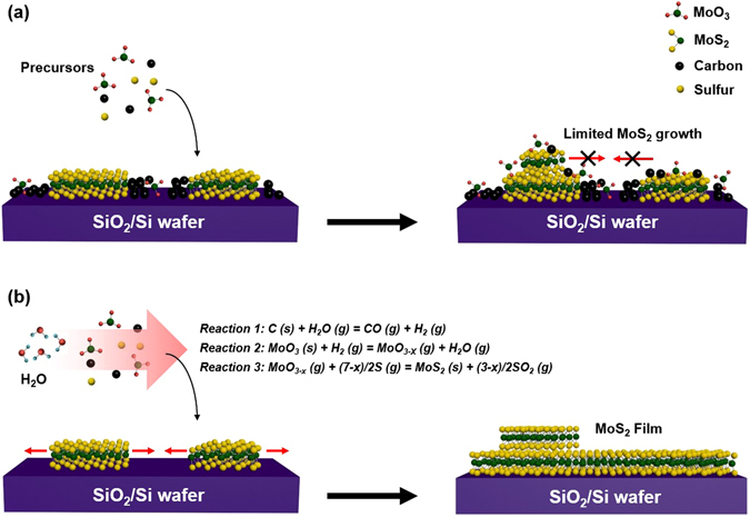
Different growth behavior. (a,b) Schematic illustration of MoS2 growth (a) without and (b) with water supply. Without water supply, unwanted impurities such as MoO3 and a-Cs inhibit the completed MoS2 film. In the presence of water, the full-covered MoS2 film is grown through Reactions 1–3.
Conclusions
We have synthesized MoS2 films using a single liquid precursor made by dissolving Mo(CO)6 in (CH3)2S2. The liquid precursor consists of Mo ions, Mo compounds and sulfur compounds. Unlike with a solid precursor, full-coverage MoS2 can be obtained simply by increasing the growth time. We found the introduction of water to be important in removing unwanted impurities, such a-C and molybdenum oxides from the MoS2 film. Carbon was removed by water oxidation in Reaction 1: C (s) + H2O (g) = CO (g) + H2 (g), and the hydrogen gas stemming from Reaction 1 helps effectively remove the molybdenum oxide. As a consequence, an impurity-free MoS2 film was grown with the assistance of water. Our approach does not only open the use of organic liquid precursors in the synthesis of MoS2 but also advances the synthesis of other s-TMdCs.
Methods
Substrate preparation
20 mm × 20 mm Si substrate with a 300 nm thick SiO2 layer was kept in Piranha solution to remove the organic residues and produce a hydrophilic surface. After rinsing and drying the substrate, 0.01 wt% PTAS solution was coated on the substrate as a seeding promoter via spin-coating. The substrate was placed on the center of a 5 cm × 5 cm quartz plate.
Preparation of the single liquid precursor
0.5 g of molybdenum hexacarbonyl (Mo(CO)6, >99.9%, Sigma Aldrich) powder was dissolved in 50 mL of dimethyl disulfide (CH3SSCH3, >99%, Sigma Aldrich). The mixture was kept in a quartz bubbler. To prevent the agglomeration, the solution was stirred with a magnetic bar on a home-made stirring system.
Growth of the MoS2 film
A furnace and a 2-inch quartz tube were connected and equipped with high-purity (99.999%) argon, hydrogen gas, and two bubblers (liquid precursor and water). The growth substrate was loaded at the center of the quartz tube. Prior to growth, the system was purged using argon at 500 sccm for 10 minutes. The quartz tube was rapidly heated up to 750 °C for 8 min in a preheated furnace. During growth, the temperature was maintained with 5 sccm of precursor and 10 sccm of water flow for 15 minutes. After growth, the quartz tube was rapidly cooled down to room temperature by taking the quartz out of the furnace. 350 sccm of argon flow rate at atmospheric pressure was maintained throughout the entire growth process.
Characterization
The liquid precursor mixture was analyzed via liquid chromatography mass spectrometry (XEVO TQ-S, Waters). The surface morphologies of MoS2 were characterized via optical microscopy (Nikon LV-IM, Nikon), scanning electron microscopy (JSM-7100F, JEOL), and atomic force microscopy (N8-NEOS, Bruker). To identify phonon vibration and photoluminescence of sample, a micro-Raman system (XperRam100, Nanobase) was used with a 532-nm laser. The laser power was kept at 0.1 mW to avoid damaging the sample. The chemical composition of MoS2 was analyzed via X-ray photoelectron spectroscopy (K-alpha, Thermo fisher scientific), and the atomic structures of MoS2 and the molybdenum oxide particles were characterized by transmission electron microscopy (Tecnai, FEI). The acceleration voltage was 200 kV during the TEM measurement. Prior to TEM measurement, the MoS2 were transferred on a TEM grid using conventional PMMA transfer48.
Electronic supplementary material
Acknowledgements
This work was supported by Basic Science Research Program through the National Research Foundation of Korea (NRF) funded by the Ministry of Science, ICT & Future Planning (2015R1C1A1A02037083) and the Korea Institute of Energy Technology Evaluation and Planning (KETEP) and the Ministry of Trade, Industry & Energy(MOTIE) of the Republic of Korea (No. 20152020001930). W.Y. acknowledges support from Basic Science Research Program through the National Research Foundation of Korea (NRF) funded by the Ministry of Education (Nos. 2015R1D1A1A01058991 and 2016R1S6A1A03012877). J.H.P. acknowledges support from the Institute for Basic Science (IBS-R011-D1). J.S.L. and S.M.K. acknowledges support from the Korea Institute of Science and Technology (KIST) Institutional Program.
Author Contributions
S.H.C., B.S. and K.K.K. designed the experiment. S.H.C. carried out most of the experiments. B.S. contributed to the chemical stability and composition analysis of the liquid precursor. J.H.P. contributed to the analysis of Raman and XPS spectra. J.S.L. and S.M.K. contributed to XPS, TEM measurements and the analysis of TEM results. S.M.K., W.Y. and K.K.K. guided the whole work and revised the manuscript. All the authors discussed the results and contributed to write the manuscript.
Competing Interests
The authors declare that they have no competing interests.
Footnotes
Electronic supplementary material
Supplementary information accompanies this paper at doi:10.1038/s41598-017-02228-8
Publisher's note: Springer Nature remains neutral with regard to jurisdictional claims in published maps and institutional affiliations.
References
- 1.Radisavljevic B, Radenovic A, Brivio J, Giacometti V, Kis A. Single-layer MoS2 transistors. Nat. Nanotechnol. 2011;6:147–150. doi: 10.1038/nnano.2010.279. [DOI] [PubMed] [Google Scholar]
- 2.Lopez-Sanchez O, Lembke D, Kayci M, Radenovic A, Kis A. Ultrasensitive photodetectors based on monolayer MoS2. Nat. Nanotechnol. 2013;8:497–501. doi: 10.1038/nnano.2013.100. [DOI] [PubMed] [Google Scholar]
- 3.Zeng HL, Dai JF, Yao W, Xiao D, Cui XD. Valley polarization in MoS2 monolayers by optical pumping. Nat. Nanotechnol. 2012;7:490–493. doi: 10.1038/nnano.2012.95. [DOI] [PubMed] [Google Scholar]
- 4.Cong CX, et al. Synthesis and Optical Properties of Large-Area Single-Crystalline 2D Semiconductor WS2 Monolayer from Chemical Vapor Deposition. Adv. Opt. Mater. 2014;2:131–136. doi: 10.1002/adom.201300428. [DOI] [Google Scholar]
- 5.Cai, Y. Q., Lan, J. H., Zhang, G. & Zhang, Y. W. Lattice vibrational modes and phonon thermal conductivity of monolayer MoS2. Phys. Rev. B89 (2014).
- 6.Bertolazzi S, Brivio J, Kis A. Stretching and Breaking of Ultrathin MoS2. Acs Nano. 2011;5:9703–9709. doi: 10.1021/nn203879f. [DOI] [PubMed] [Google Scholar]
- 7.Mak, K. F., Lee, C., Hone, J., Shan, J. & Heinz, T. F. Atomically Thin MoS2: A New Direct-Gap Semiconductor. Phys. Rev. Lett. 105 (2010). [DOI] [PubMed]
- 8.Ross JS, et al. Electrically tunable excitonic light-emitting diodes based on monolayer WSe2 p-n junctions. Nat. Nanotechnol. 2014;9:268–272. doi: 10.1038/nnano.2014.26. [DOI] [PubMed] [Google Scholar]
- 9.Splendiani A, et al. Emerging Photoluminescence in Monolayer MoS2. Nano Lett. 2010;10:1271–1275. doi: 10.1021/nl903868w. [DOI] [PubMed] [Google Scholar]
- 10.Bao, W. Z., Cai, X. H., Kim, D., Sridhara, K. & Fuhrer, M. S. High mobility ambipolar MoS2 field-effect transistors: Substrate and dielectric effects. Appl. Phys. Lett. 102 (2013).
- 11.Amani M, et al. Near-unity photoluminescence quantum yield in MoS2. Science. 2015;350:1065–1068. doi: 10.1126/science.aad2114. [DOI] [PubMed] [Google Scholar]
- 12.Voiry D, et al. Conducting MoS2 Nanosheets as Catalysts for Hydrogen Evolution Reaction. Nano Lett. 2013;13:6222–6227. doi: 10.1021/nl403661s. [DOI] [PubMed] [Google Scholar]
- 13.Xie JF, et al. Defect-Rich MoS2 Ultrathin Nanosheets with Additional Active Edge Sites for Enhanced Electrocatalytic Hydrogen Evolution. Adv. Mater. 2013;25:5807–+. doi: 10.1002/adma.201302685. [DOI] [PubMed] [Google Scholar]
- 14.Wu ZZ, et al. Acs. Catal. 2013. MoS2 Nanosheets: A Designed Structure with High Active Site Density for the Hydrogen Evolution Reaction; pp. 2101–2107. [Google Scholar]
- 15.Lee GH, et al. Flexible and Transparent MoS2 Field-Effect Transistors on Hexagonal Boron Nitride-Graphene Heterostructures. Acs Nano. 2013;7:7931–7936. doi: 10.1021/nn402954e. [DOI] [PubMed] [Google Scholar]
- 16.Yoon J, et al. Highly Flexible and Transparent Multilayer MoS2 Transistors with Graphene Electrodes. Small. 2013;9:3295–3300. doi: 10.1002/smll.201300134. [DOI] [PubMed] [Google Scholar]
- 17.He QY, et al. Fabrication of Flexible MoS2 Thin-Film Transistor Arrays for Practical Gas-Sensing Applications. Small. 2012;8:2994–2999. doi: 10.1002/smll.201201224. [DOI] [PubMed] [Google Scholar]
- 18.Wan W, et al. Interlayer coupling of a direct van der Waals epitaxial MoS2/graphene heterostructure. Rsc Adv. 2016;6:323–330. doi: 10.1039/C5RA22768B. [DOI] [Google Scholar]
- 19.Tan LK, et al. Atomic layer deposition of a MoS2 film. Nanoscale. 2014;6:14002–14002. doi: 10.1039/C4NR90076F. [DOI] [PubMed] [Google Scholar]
- 20.Lee YH, et al. Synthesis of Large-Area MoS2 Atomic Layers with Chemical Vapor Deposition. Adv. Mater. 2012;24:2320–2325. doi: 10.1002/adma.201104798. [DOI] [PubMed] [Google Scholar]
- 21.Ling X, et al. Role of the Seeding Promoter in MoS2 Growth by Chemical Vapor Deposition. Nano Lett. 2014;14:464–472. doi: 10.1021/nl4033704. [DOI] [PubMed] [Google Scholar]
- 22.Najmaei S, et al. Vapour phase growth and grain boundary structure of molybdenum disulphide atomic layers. Nat. Mater. 2013;12:754–759. doi: 10.1038/nmat3673. [DOI] [PubMed] [Google Scholar]
- 23.van der Zande AM, et al. Grains and grain boundaries in highly crystalline monolayer molybdenum disulphide. Nat. Mater. 2013;12:554–561. doi: 10.1038/nmat3633. [DOI] [PubMed] [Google Scholar]
- 24.Yu, Y. F. et al. Controlled Scalable Synthesis of Uniform, High-Quality Monolayer and Few-layer MoS2 Films. Sci. Rep. 3, doi: 10.1038/srep01866 (2013). [DOI] [PMC free article] [PubMed]
- 25.Shi YM, et al. van der Waals Epitaxy of MoS2 Layers Using Graphene As Growth Templates. Nano Lett. 2012;12:2784–2791. doi: 10.1021/nl204562j. [DOI] [PubMed] [Google Scholar]
- 26.Ji QQ, et al. Epitaxial Monolayer MoS2 on Mica with Novel Photoluminescence. Nano Lett. 2013;13:3870–3877. doi: 10.1021/nl401938t. [DOI] [PubMed] [Google Scholar]
- 27.Lin YC, et al. Direct Synthesis of van der Waals Solids. Acs Nano. 2014;8:3715–3723. doi: 10.1021/nn5003858. [DOI] [PubMed] [Google Scholar]
- 28.Lee Y, et al. Synthesis of wafer-scale uniform molybdenum disulfide films with control over the layer number using a gas phase sulfur precursor. Nanoscale. 2014;6:2821–2826. doi: 10.1039/c3nr05993f. [DOI] [PubMed] [Google Scholar]
- 29.Tran, B. T. et al. Direct Growth and Controlled Coalescence of Thick AlN Template on Micro-circle Patterned Si Substrate. Sci. Rep. 5, doi:10.1038/srep14734 (2015). [DOI] [PMC free article] [PubMed]
- 30.Lee KJ, et al. A printable form of single-crystalline gallium nitride for flexible optoelectronic systems. Small. 2005;1:1164–1168. doi: 10.1002/smll.200500166. [DOI] [PubMed] [Google Scholar]
- 31.Kang K, et al. High-mobility three-atom-thick semiconducting films with wafer-scale homogeneity. Nature. 2015;520:656–660. doi: 10.1038/nature14417. [DOI] [PubMed] [Google Scholar]
- 32.Li H, et al. From Bulk to Monolayer MoS2: Evolution of Raman Scattering. Advanced Functional Materials. 2012;22:1385–1390. doi: 10.1002/adfm.201102111. [DOI] [Google Scholar]
- 33.Kim KK, et al. Synthesis of Monolayer Hexagonal Boron Nitride on Cu Foil Using Chemical Vapor Deposition. Nano Lett. 2012;12:161–166. doi: 10.1021/nl203249a. [DOI] [PubMed] [Google Scholar]
- 34.Hata K, et al. Water-Assisted Highly Efficient Synthesis of Impurity-Free Single-Walled Carbon Nanotubes. Science. 2004;306:1362–1364. doi: 10.1126/science.1104962. [DOI] [PubMed] [Google Scholar]
- 35.Wagman, D. D., Kilpatrick, J. E. & Taylor, W. J. Heats, free energies, and equilibrium constants of some reactions involving O2, H2, H2O, C, CO, CO2, and CH4. (U. S. Govt. print. off., 1945).
- 36.Kim, S. M. et al. Synthesis of large-area multilayer hexagonal boron nitride for high material performance. Nat. Commun. 6, doi:10.1038/ncomms9662 (2015). [DOI] [PMC free article] [PubMed]
- 37.Bhanu, U., Islam, M. R., Tetard, L. & Khondaker, S. I. Photoluminescence quenching in gold - MoS2 hybrid nanoflakes. Sci. Rep. 4, doi:10.1038/srep05575 (2014). [DOI] [PMC free article] [PubMed]
- 38.Kang NR, Paudel HP, Leuenberger MN, Tetard L, Khondaker SI. Photoluminescence Quenching in Single-Layer MoS2 via Oxygen Plasma Treatment. J. Phys. Chem. C. 2014;118:21258–21263. doi: 10.1021/jp506964m. [DOI] [Google Scholar]
- 39.Mak KF, et al. Tightly bound trions in monolayer MoS2. Nat. Mater. 2013;12:207–211. doi: 10.1038/nmat3505. [DOI] [PubMed] [Google Scholar]
- 40.Mouri S, Miyauchi Y, Matsuda K. Tunable Photoluminescence of Monolayer MoS2 via Chemical Doping. Nano Lett. 2013;13:5944–5948. doi: 10.1021/nl403036h. [DOI] [PubMed] [Google Scholar]
- 41.Zangwill, A. Physics at surfaces. (Cambridge University Press, 1988).
- 42.Eda G, et al. Photoluminescence from Chemically Exfoliated MoS2. Nano Lett. 2011;11:5111–5116. doi: 10.1021/nl201874w. [DOI] [PubMed] [Google Scholar]
- 43.Zhang H, et al. Organic-Inorganic Hybrid Materials Based on Basket-like {Ca subset of P6Mo18O73} Cages. Inorg. Chem. 2015;54:6744–6757. doi: 10.1021/acs.inorgchem.5b00508. [DOI] [PubMed] [Google Scholar]
- 44.Hu B, Mai LQ, Chen W, Yang F. From MoO3 Nanobelts to MoO2 Nanorods: Structure Transformation and Electrical Transport. Acs Nano. 2009;3:478–482. doi: 10.1021/nn800844h. [DOI] [PubMed] [Google Scholar]
- 45.McCarron EM, III, Calabrese JC. The growth and single crystal structure of a hihg pressure phase of molybdenum trioxide: MoO3-II. J. Solid State Chem. 1991;91:121–125. doi: 10.1016/0022-4596(91)90064-O. [DOI] [Google Scholar]
- 46.Parise JB, McCarron EM, III, Sleight W. A new modification of ReO3-type MoO3 and the deuterated intercalation compound from which it is derived: D0.99MoO3. Mater. Res. Bull. 1987;22:803–811. doi: 10.1016/0025-5408(87)90035-3. [DOI] [Google Scholar]
- 47.Kang J, et al. Thickness sorting of two-dimensional transition metal dichalcogenides via copolymer-assisted density gradient ultracentrifugation. Nat. Commun. 2014;5:5478. doi: 10.1038/ncomms6478. [DOI] [PubMed] [Google Scholar]
- 48.Regan W, et al. A direct transfer of layer-area graphene. Appl. Phys. Lett. 2010;96:113102. doi: 10.1063/1.3337091. [DOI] [Google Scholar]
Associated Data
This section collects any data citations, data availability statements, or supplementary materials included in this article.


