Abstract
Nanoelectronic devices integrated with dielectrophoresis (DEP) have been promoted as promising platforms for trapping, separating, and concentrating target biomarkers and cancer cells from a complex medium. Here, we visualized DEP and DEP gradients in conventional nanoelectronic devices by using multi-pass atomic force microcopy techniques. Our measurements directly demonstrated a short range DEP only at sharp step edges of electrodes, frequency dependent DEP polarity, and separation distance dependent DEP strength. Additionally, non-uniform DEP along the edges of the electrodes due to a large variation in electric field strength was observed. The strength and apparent working distance of DEP were measured to be an order of a few nN and 80 nm within the limited scale of particles and other parameters such as an ionic strength of the medium. This method provides a powerful tool to quantify the strength and polarity of DEP and allows optimizing and calibrating the device's operating parameters including the driving field strength for the effective control and manipulation of target biomolecules.
Recent advances in biotechnology have allowed capturing individual biomolecules including disease-markers and cancer cells and monitoring their biological activities.1–4 The ultimate goal of this field would be to completely control and manipulate the biomolecules for practical diagnostic applications. Among a number of techniques developed for the detection and manipulation of biomolecules, dielectrophoresis (DEP)-based methods have demonstrated the feasibility of a remote control of target molecules to trap and dissect for highly sensitive screening. For example, DEP has been used for the separation of yeast cells,5 viruses,6 and cancer cells,1,7 as well as to trap particular DNA molecules,8,9 providing tremendous potential in biomedical applications.
In principle, DEP is a force exerted on a polarizable particle such as biomolecules and cells in the presence of non-uniform AC electric fields in liquid medium.10 Depending on the dielectric responses of the particle and the surrounding medium, the external fields induce an effective dipole moment p on the particle and an instantaneous force FDEP = p · ∇E, acting on the dipole.11,12 For the particle suspended in the non-uniform fields, the net force does not vanish. Thus, spatially asymmetric force due to the inhomogeneous field gradient in the medium drives the movement of the particle. In general, the force can be used to selectively attract (attractive FDEP) or repel (repulsive FDEP) biomolecules of interest from a complex medium to regions of strong electric fields. For example, cancer cells,13 cellular components,1 and biomarkers14,15 can be collected, separated, concentrated, and transported using DEP-based micro-fluidic devices.
Although such non-invasive, non-contact DEP manipulation is a promising platform for biomedical applications, measuring and determining the strength of FDEP on biomolecules in nanoelectronic devices are challenging problems. In addition, several issues associated with DEP limit its applicability in practice. First, the external AC field intensity and its frequency to generate bipolar DEP can cause unwanted electrochemical reactions such as water electrolysis at metal electrodes,8 destroying both the biological sample and the nanoelectronic devices. Second, FDEP may not be uniformly distributed in the electrodes patterned on the devices due to the high sensitivity of the field variations near the sharp corners or edges of the electrodes at the nanoscale.16 Effective solutions to the problems, on the other hand, would help to design the nanoelectronic device and tune the operating parameters to achieve strong FDEP to effectively manipulate target biomolecules in a desired manner under physiological conditions.
Here, we show that FDEP in the nanoelectronic devices can be experimentally measured and quantitatively evaluated by atomic force microscopy (AFM). A non-contact, dynamic AC lift-mode AFM method similar to the typical electric or magnetic force measurement methods17,18 was used to investigate the force between an AFM probe tip and the nanoelectronic devices including both the smooth surface and the sharp edges of electrodes. The measurements allowed mapping out the force variation along the direction (z) normal to the electrode surface in the device.
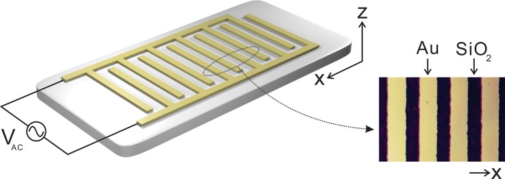
In this work, the conventional interdigitated electrode array that has proven to be quite useful for dielectrophoretic separation and travelling wave dielectrophoresis in previous research studies19,20 was examined as shown in Fig. 1. The device consists of planar metallic electrode arrays on a SiO2 substrate. With a pre-patterned mylar mask, gold electrodes were defined by the standard optical lithography, similar to the previous study.21 The width of electrodes, gaps between the electrodes, and the height of the electrodes were 16 μm, 10 μm, and 140 nm, respectively.
FIG. 1.
Schematic of an interdigitated metal (Au) electrode array connected to the AC voltage source.
Devices were mounted in a liquid-compatible commercial AFM (NT-MDT NTEGRA AFM), and the AFM imaging was performed in an ionic buffer solution without evaporation while measuring. Conventional silicon AFM probe tips without a coating (force constant = 2.7 N/m, Budget sensors) were used for the imaging. The external AC voltage between the two metal electrodes was applied by a commercial function/arbitrary waveform generator (Agilent 33220A), which was filtered and synchronized with the AFM scanning. A multi-pass scanning technique was employed for the precise measurements of both surface topography and the force gradient. The first-pass scanning was performed in the typical semi-contact mode to obtain the surface topography characteristics. During the second-pass measuring the force gradient, the probe was raised above the surface at a distance z followed by the surface topography contour. Such lift-mode scanning in the second-pass prevents any influence of surface features on the measurement.
The second-pass measurement depends solely on the force gradient along the z direction based on the point probe approximation assuming that the probe tip has a dipole moment located in the center of the tip end. The AC lift-mode operates with a lock-in feedback loop to keep driving the probe oscillation at the nearly resonance frequency.17,22 When a force acts on the probe tip, it causes the resonance frequency of the tip to shift, depending on the force gradient and the direction. Additionally, such changes in resonance frequency result in an amplitude and phase shift. Thus, although the three parameters serve as an indicator of the force measurement, the force gradient is mainly detected by measuring the probe tip's phase vibration in the amplitude modulation mode using a simple lock-in amplifier. A mathematical relationship between the phase shift and the force gradient when ∂F/∂z is very small in magnitude compared to k is given by
| (1) |
where Q is the Q-factor of the resonance peak, k is the force constant of the probe tip, and ∂F/∂z is the force gradient in the direction normal to the surface.23,24 When ∂F/∂z is measured according to z, F can be obtained by integrating ∂F/∂z. For example, the negative shift of the measured phase corresponds to the attractive F and negative ∂F/∂z along the z direction.
The AFM measurements were carried out in a phosphate buffer (1–10 μM KH2PO4, pH 7) at room temperature. The ionic strength of the buffer and the amplitude and frequency of the applied AC voltage were determined by the classical Maxwell-Wagner (MW) theory.10,11 Specifically, the complex Clausius-Mossotti (CM) factor depending on the complex permittivities of the particle and suspending medium and a depolarizing factor of the particle allow estimating the frequency dependent effective dipole moments of the particles as well as the magnitude and polarity of FDEP (see Figs. S1 and S2 in the supplementary material). The CM factor for the spherical and ellipsoidal geometry is discussed in the supplementary material.
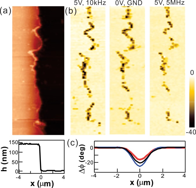
Figure 2 depicts typical multi-pass AFM images of the device in the absence and in the presence of the external AC fields (Vac). Figure 2(a) presents a topography image and the corresponding height profile of the device acquired during the first-pass scanning, while the Vac was in the off-mode. The metal electrodes and SiO2 substrates were relatively flat and smooth compared to the sharp edge of the electrodes in the image. The edge line of the electrode is highly disordered at the nanoscale, producing additional non-uniform electric field distributions due to the lighting rod effects.16 During the second-pass, lift-mode scanning at a particular z, a sinusoidal wave form of Vac with a peak to peak potential of 5 V is applied through the two electrodes (Fig. 1) to examine the AC field effects. Figure 2(b) shows the phase images of the same electrode [Fig. 2(a)] under three different conditions: Vac (5 Vpp, 10 kHz); Vac (0 V, GND); and Vac (5 Vpp, 5 MHz) at z = 20 nm.
FIG. 2.
Multi-pass AFM measurements. (a) A topography image of the metal electrode (red color) and the SiO2 (black color) substrate and a height profile of line-cuts of the cross-section. (b) Phase images of (a) at three Vac fields. (c) The averaged phase shifts along the electrode step edge. Blue, black, and red curves correspond to 10 kHz, GND, and 5 MHz fields, respectively.
In the control measurements performed without the external AC field (Vac = 0 V), the phase shift was observed along the electrode edge direction. Such a phase shift is attributed to a geometry effect at the sharp step edge. When the AFM scans over the step edge, the distance z between the tip and the sample instantly decreases and brings the tip into a more negative force gradient until the feedback loop restores the initial distance z.22 Therefore, the negative force gradient due to the attractive force variations is shown in the dark color phase image only at the edge.
When the AC electric fields were applied with different frequencies, further phase shifts were observed as depicted in Fig. 2(b). In the presence of Vac (10 kHz), the features along the edge line in the phase image were unchanged, but their color was revealed to be darker, reflecting additional attractive forces acting on the AFM tip. Thus, the low frequency AC fields generated the attractive FDEP and negative ∂FDEP/∂z. In contrast, repulsive FDEP generated by the high frequency (5 MHz) fields reduced the net force, resulting in the brighter edge line in Fig. 2(b). Figure 2(c) compares the mean phase shift along the edge direction for each measurement. Taken together, the frequency dependent, binary FDEP effects were able to be measured by our multi-pass AFM experiments.
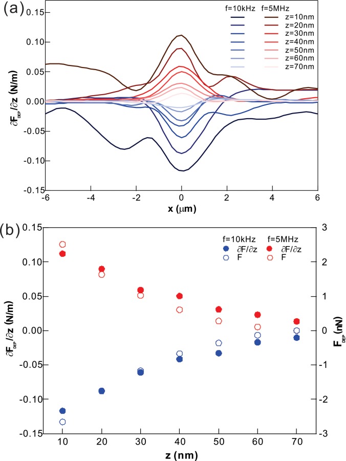
To examine the spatial distribution of FDEP and ∂FDEP/∂z along the x and z directions, the AFM measurements were carried out by varying z across the electrodes with two fixed frequencies of 10 kHz (attractive FDEP) and 5 MHz (repulsive FDEP). Figure 3(a) displays pure ∂FDEP/∂z components and their z dependence, where the background component without the AC fields was removed at each z. Both positive and negative ∂FDEP/∂z peaked at the edge of the electrode (x = 0) for all z. The magnitude of ∂FDEP/∂z fell off along the x axis regardless of the sign of ∂FDEP/∂z and z, suggesting the reduction in the field strength variations along the x axis. Finally, the magnitude of ∂FDEP/∂z approached minimum values when the tip was away from the edge (|x| > 0), indicating minimum points in the field strength at the top of the electrode and a point equidistant between two electrodes. Such observations are in excellent agreement with the strong dependence of FDEP on the strength of field gradients (FDEP ∝ ∇E2).11
FIG. 3.
The spatial distribution of ∂FDEP/∂z. (a) The average ∂FDEP/∂z versus two driving (10 kHz and 5 MHz) frequencies, demonstrating attractive FDEP with 10 kHz and repulsive FDEP with 5 MHz. (b) The average ∂FDEP/∂z and FDEP versus the separation distance z. FDEP was obtained by integrating ∂FDEP/∂z.
Figure 3(b) displays the peak values of ∂FDEP/∂z and FDEP calculated from the measured ∂FDEP/∂z as a function of z.17 The values were nonlinearly decreased upon increasing the separation distance z between the tip and the electrode edge. The shape of these curves suggests the nonlinear changes in the intensity of the field gradient at the edge. Furthermore, the magnitude of FDEP and ∂FDEP/∂z was almost identical for two different frequencies at the same z. The results indicate that the CM factors for the low (10 kHz) and high (5 MHz) frequencies are nearly identical, which is further supported by our CM calculation (Fig. S1, supplementary material). When the tip was further away from the edge (>80 nm), FDEP approached nearly zero, providing an upper limit for the working distance of the short-range FDEP.
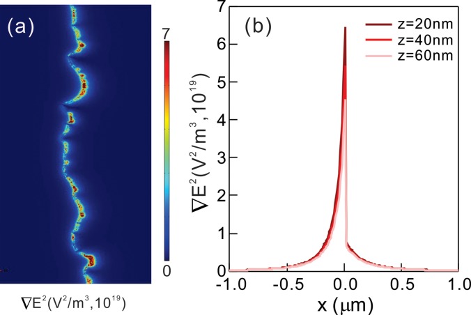
To further support our experimental observation, the fields and the field gradients were generated using commercial finite element software, COMSOL Multiphysics (COMSOL Inc.),21 under identical conditions used in the experimental measurements (see supplementary material). Figure 4 presents the spatial distributions of the fields and the strength of the gradient of the fields ∇E2 over and across the electrode. The large variations in the fields appeared at the sharp edge, which was in strong agreement with our experimental observations. An asymmetric shape of the gradient of the field is due to the non-uniform charge distribution near the electrode edge. Furthermore, the magnitude of field gradients decreases as z increases, confirming the separation distance-dependent, short-range DEP that is observed experimentally.
FIG. 4.
(a) A two dimensional plot of the strength of the gradient fields and (b) its profile along the x direction at various z values generated by COMSOL Multiphysics simulations.
Previous studies performed with both micro-scale particles and electrodes have revealed that FDEP was sufficient to drive motions of the particles.25–27 When the particle size decreases to the nanoscale, however, FDEP substantially decreases due to the particle volume dependence of FDEP (FDEP ∝ R3). Thus, although FDEP can be either repulsive or attractive by the driving frequency of the fields, our results proved that the strength and the apparent working distance of FDEP were strongly dependent on both particles' dimension and electrodes' fine structure.
In conclusion, we achieved quantitative measurements of FDEP and ∂FDEP/∂z in conventional, nanoscale, electronic devices using the multi-pass AFM methods. The results provided the spatial distribution of DEP and its strong dependence on the nanoscale structure of the electrode and the nanoscale separation distance from the electrode edge. On this scale, precise measurements of DEP are more important for quantitative comparisons among the competing forces such as viscous drag, Brownian, and hydrodynamic forces to determine the dominant forces governing the movements of biomolecules. Thus, the present study could benefit further development of DEP-based sensors and detectors for nanoscale proteins and biomarkers. For example, DEP could be integrated with conventional field effect transistor-based biosensors to lower the detection limit of target molecules on a rapid timescale. Alternatively, DEP could be used to pre-screen and filter the target/non-target molecules in microfluidic devices to maximize detection sensitivity or minimize interference from the non-target molecules in the blood sample. The development of such techniques demands precise knowledge of DEP to design nanoelectronic devices and tune the operating parameters associated with other interfering forces for the effective manipulation of the target molecules.
See supplementary material for the CM factor and COMSOL Multiphysics calculation.
Acknowledgments
This research was supported financially by the National Institute of General Medical Sciences of the National Institutes of Health under Award No. R15GM122063.
References
- 1. Voldman J., Annu. Rev. Biomed. Eng. 8, 425–454 (2006). 10.1146/annurev.bioeng.8.061505.095739 [DOI] [PubMed] [Google Scholar]
- 2. Zheng G., Patolsky F., Cui Y., Wang W. U., and Lieber C. M., Nat. Biotechnol. 23, 1294–1301 (2005). 10.1038/nbt1138 [DOI] [PubMed] [Google Scholar]
- 3. Joo C., Balci H., Ishitsuka Y., Buranachai C., and Ha T., Annu. Rev. Biochem. 77, 51–76 (2008). 10.1146/annurev.biochem.77.070606.101543 [DOI] [PubMed] [Google Scholar]
- 4. Stern E., Vacic A., Rajan N. K., Criscione J. M., Park J., Ilic B. R., Mooney D. J., Reed M. A., and Fahmy T. M., Nat. Nanotechnol. 5, 138–142 (2010). 10.1038/nnano.2009.353 [DOI] [PMC free article] [PubMed] [Google Scholar]
- 5. Pethig R., Crit. Rev. Biotechnol. 16, 331–348 (1996). 10.3109/07388559609147425 [DOI] [Google Scholar]
- 6. Morgan H., Hughes M. P., and Green N. G., Biophys. J. 77, 516–525 (1999). 10.1016/S0006-3495(99)76908-0 [DOI] [PMC free article] [PubMed] [Google Scholar]
- 7. Li H. and Bashir R., Sens. Actuators, B 86, 215–221 (2002). 10.1016/S0925-4005(02)00172-7 [DOI] [Google Scholar]
- 8. Chou C.-F., Tegenfeldt J. O., Bakajin O., Chan S. S., Cox E. C., Darnton N., Duke T., and Austin R. H., Biophys. J. 83, 2170–2179 (2002). 10.1016/S0006-3495(02)73977-5 [DOI] [PMC free article] [PubMed] [Google Scholar]
- 9. Washizu M. and Kurosawa O., IEEE Trans. Ind. Appl. 26, 1165–1172 (1990). 10.1109/28.62403 [DOI] [Google Scholar]
- 10. Pohl H. A., Dielectrophoresis: The Behavior of Neutral Matter in Nonuniform Electric Fields ( Cambridge University Press, Cambridge, 1978). [Google Scholar]
- 11. Jones T. B., Electromechanics of Particles ( Cambridge University Press, Cambridge, 1995). [Google Scholar]
- 12. Gascoyne P. R. C. and Vykoukal J., Electrophoresis 23, 1973–1983 (2002). [DOI] [PMC free article] [PubMed] [Google Scholar]
- 13. Becker F. F., Wang X. B., Huang Y., Pethig R., Vykoukal J., and Gascoyne P. R., Proc. Natl. Acad. Sci. U.S.A. 92, 860–864 (1995). 10.1073/pnas.92.3.860 [DOI] [PMC free article] [PubMed] [Google Scholar]
- 14. Jones T. B., IEEE Eng. Med. Biol. 22, 33–42 (2003). 10.1109/MEMB.2003.1304999 [DOI] [PubMed] [Google Scholar]
- 15. Gong J.-R., Small 6, 967–973 (2010). 10.1002/smll.200902132 [DOI] [PubMed] [Google Scholar]
- 16. Jackson J., Classical Electrodynamics, 3rd ed. ( Wiley, 1998). [Google Scholar]
- 17. Martin Y. and Wickramasinghe H. K., Appl. Phys. Lett. 50, 1455–1457 (1987). 10.1063/1.97800 [DOI] [Google Scholar]
- 18. Nonnenmacher M., O'Boyle M. P., and Wickramasinghe H. K., Appl. Phys. Lett. 58, 2921–2923 (1991). 10.1063/1.105227 [DOI] [Google Scholar]
- 19. Ramos A., Morgan H., Green N. G., and Castellanos A., J. Phys. D: Appl. Phys. 31, 2338 (1998). 10.1088/0022-3727/31/18/021 [DOI] [Google Scholar]
- 20. Hywel M., Alberto García I., David B., Nicolas G. G., and Antonio R., J. Phys. D: Appl. Phys. 34, 1553 (2001). 10.1088/0022-3727/34/10/316 [DOI] [Google Scholar]
- 21. Velmanickam L., Laudenbach D., and Nawarathna D., Phys. Rev. E 94, 042408 (2016). 10.1103/PhysRevE.94.042408 [DOI] [PubMed] [Google Scholar]
- 22. Voigtländer B., Scanning Probe Microscopy: Atomic Force Microscopy and Scanning Tunneling Microscopy ( Springer-Verlag, Berlin, Heidelberg, New Nork, 2015). [Google Scholar]
- 23. Martin Y., Williams C. C., and Wickramasinghe H. K., J. Appl. Phys. 61, 4723–4729 (1987). 10.1063/1.338807 [DOI] [Google Scholar]
- 24. Magonov S. N., Elings V., and Whangbo M. H., Surf. Sci. 375, L385–L391 (1997). 10.1016/S0039-6028(96)01591-9 [DOI] [Google Scholar]
- 25. Green N. G. and Morgan H., J. Phys. Chem. B 103, 41–50 (1999). 10.1021/jp9829849 [DOI] [Google Scholar]
- 26. Wei M.-T., Junio J., and Ou-Yang H. D., Biomicrofluidics 3, 012003 (2009). 10.1063/1.3058569 [DOI] [PMC free article] [PubMed] [Google Scholar]
- 27. Imasato H. and Yamakawa T., J. Electrophoresis 52, 1–8 (2008). 10.2198/jelectroph.52.1 [DOI] [Google Scholar]
Associated Data
This section collects any data citations, data availability statements, or supplementary materials included in this article.
Supplementary Materials
See supplementary material for the CM factor and COMSOL Multiphysics calculation.


