

Abstract
The detector in single-photon emission computed tomography has played a key role in the quality of the images. Over the past few decades, developments in semiconductor detector technology provided an appropriate substitution for scintillation detectors in terms of high sensitivity, better energy resolution, and also high spatial resolution. One of the considered detectors is cadmium telluride (CdTe). The purpose of this paper is to review the CdTe semiconductor detector used in preclinical studies, small organ and small animal imaging, also research in nuclear medicine and other medical imaging modalities by a complete inspect on the material characteristics, irradiation principles, applications, and epitaxial growth method.
Keywords: Cadmium telluride, image quality, radiation detector, semiconductor, single-photon emission computed tomography
Introduction
There are different approaches and also materials to construct a detector for single-photon emission computed tomography (SPECT) imaging system. Irrespective of the approach, the aim is to transform the energy of gamma-ray photons into an electrical signal.[1] There are two common groups of solid materials applied to a detector system including scintillators and semiconductors.[2] Currently, the scintillators are generally used in nuclear medicine. There are usually either inorganic salts or organic substances in the forms of solid crystals.[3,4] Thallium-doped sodium iodide [NaI(Tl)] or thallium-doped cesium iodide and so bismuth germinate and lanthanum bromide activated by cerium are the examples of scintillation substrate. The scintillator detectors convert the gamma-ray photons to the visible photons, and then, the visible photons are converted into an electrical signal. Besides, semiconductor materials such as cadmium telluride (CdTe) and cadmium zinc telluride (CdZnTe) are important alternatives for the scintillation detector, known as solid state detectors. In the detectors, gamma-ray photons caused electron-hole pairs and electrical charge drift to opposite directions using an electric field, then induce signals on electrodes, and directly create electrical current.[1,4,5,6] On the other hand, ionization detectors and ionization chambers use gas as the interested medium. Gas detectors convert absorbed photon energy into electron-ion pairs that move toward electrodes. The detectors are low-efficiency detectors for counting gamma rays because of their low light interaction chance and their poor capability to quantify the energy of photons. However, this approach is not used in SPECT imaging systems.[1,2,6]
Many studies have been done for improvement of SPECT devices and the image quality.[7,8] Detector plays a critical role in the quality of the created images in the medical imaging system. Furthermore, it is responsible for absorbing and detecting the high-energy photons emitted from the patient and also providing the location of the photon interaction for the photomultiplier tube (PMT) circuit.[1,5]
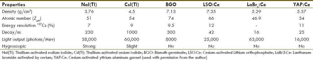
Conventional SPECT system is mostly based on NaI(Tl) as main component of photon interaction, with a high luminous efficiency, and is costly effective.[1,5,9] However, it has some limitations such as low-energy resolution, low intrinsic spatial resolution, and hygroscopic.[5,10,11] The low intrinsic spatial resolution is confined by its low density (3.76 g/cm3)[10,12,13,14] and low-energy resolution related to the abundant PMTs needed for the positioning circuit. Due to the large and massive scheme of the conventional camera, it is generally difficult to position it as near the organ and to obtain the appropriate view. This complication is exacerbated by the essence of a dead zone of some centimeter at the sides of the camera. In cases of small organ and small animal imaging, the limitation is especially important.[1,9,15] Some characteristics of the scintillators which are used, or under study and progress, for gamma-ray detection in medical imaging are presented in Table 1.[12,16]
Table 1.
Some important characteristics of scintillator crystals under development and currently used to create imaging detectors (used with some modification from the references 12 and 16)
One of the initial goals of medical imaging is to reach high detection efficiency with maintenance of a proper energy resolution. Today, research on semiconductor detectors is increasing to improve the energy resolution and intrinsic spatial resolution of the imaging systems.[2,17,18] The main objective of this paper is to review CdTe semiconductor with a favorable feature that has been used in clinical and preclinical nuclear medicine imaging and also other fields.
Semiconductor Detectors
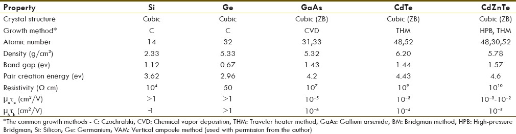
Semiconductor detectors are the main substitute for the scintillation detectors in medical imaging systems.[19,20] Silicon (Si) and germanium (Ge) materials were old semiconductors studied by Van Heerden in 1945 as radiation detectors.[17] These detectors, in comparison with the scintillators, have a lower carrier creation energy and low scatter count.[7,21] Unfortunately, Si with a low stopping power for high-energy photons is restricted to low-energy photons. Besides, Ge works at cryogenic temperatures because of its small band gap.[10,20,22,23] For these reasons, materials with a high atomic number and ability to function at room temperature such as compound semiconductors were introduced. Table 2 shows the physical features of the semiconductors that were commonly used for radiation detection.[17] CdTe and CdZnTe are probable materials for using in X and gamma rays detectors.[21,24] The strong absorption and great detection efficiency for energetic photons were provided by the high effective atomic number and density.[11] Compound semiconductors are commonly taken from the atoms of Groups II and VI (e.g. CdTe) and Groups III and V (e.g. gallium arsenide [GaAs]) in the periodic table.[17] When the material reaches to the semi-insulating condition with electrical compensation, the wide band gap of the materials permits to the formation of highly resistive tools, great depletion depths, and a few leakage currents.[9,21,25,26,27,28] Most band gaps for semiconductors as radiation detectors fall within the ranges of 0.7 to about 3 eV.[2] Ogawa et al. assessed an ultra-high resolution SPECT system equipped with a semiconductor detector.[27] They found that the energy resolution of the detector is superior to the NaI(Tl) scintillation detector; also the related intrinsic resolution was found to be the same as the pixel size due to the individual collection of the photon per pixel.[12] Improvement in energy resolution would be advantageous for an appropriate discrimination of the gamma rays that arrive to the detector and would be scored as a method for scatter rejection to improve SPECT measurements. Besides, the excellent sensitivity of these detectors caused to decrease in statistical noise and to increase in the count rate and possibly imaging at a little time with low administered radiation dose. In addition, semiconductor detector eliminates the need for bulky PMTs and so provides a thin and lightweight camera head with decreased shielding so flexible to design the camera in different shapes; besides, SPECT imaging scanners with semiconductor detector can be built very compact due to direct photon conversion and have not PMTs.[1,10,13,16,18,26,27,29,30]
Table 2.
Physical properties of the typical semiconductors at 25°C (used with some modification from the references 16 and 17)
Cadmium Telluride Detector
CdTe has been studied as the detector material since 1960s.[17] CdTe is cubic zinc blende. Its useful properties consist of a wide band gap (1.44 eV) with a high resistance (109 Ω),[2] high atomic number (Cd: 48 and Te: 52), and high density (5.85 g/cm3) which provide a better absorption characteristics.[31,32] Because of the high absorption, CdTe can be applied for detection of energetic photons. Absorption of photons in the material can be computed by the following formula:

where I is the primary intensity of photon flow, μ is the linear attenuation coefficient, and t the thickness of the absorber. For gamma-ray interactions, the linear attenuation coefficient demonstrates the absorption ability of the material per unit thickness. Commonly, the attenuation is indicated by the mass attenuation coefficient, μ/ρ, wherein ρ is the density of the substrate (g/cm3).[5,19] Figure 1 shows the linear attenuation coefficients as a function of photon energy for CdTe, NaI(Tl), Ge, and Si detector materials.[11] To obtain excellent detection efficiency with a partly thin crystal, the attenuation coefficient must be sufficient.[1] As shown in Figure 1, for similar conditions, attenuation coefficient in CdTe is higher than the others.[11] The detection efficiency for a radiation detector determines the percentage of incident detectable photons.[2] The intrinsic performance of detection is controlled by the different approaches; first, detection efficiency increases with the detector thickness. The detection efficiency of the materials versus detector thickness is shown in Figure 2. CdTe detector with various thicknesses at 140 KeV gamma rays has a greater photoelectric attenuation coefficient which gives excellent detection efficiency. Figure 3 illustrates the efficiency of 1 mm CdTe detector as a function of photon energy. In practice, this detector has approximately 32% efficiency for 140 KeV gamma rays.[11] Second, the efficiency rises with a mass density of the substrate. Ultimately, the efficiency generally increases with the atomic number (Z).[2] In a study on the performances of CdTe semiconductor and NaI(Tl) scintillation detectors, Limousin found that utilizing CdTe had benefits of improving count rate, excellent linearity, and great stability in comparison with NaI(Tl).[10,33] The detector high-efficiency yields from high atomic number and a wide band gap specify the required time and amount of injected radioactivity.[13] The lower mobility and the related carrier lifetime of holes (μhτh= 10−4 cm2/V) in comparison with electrons (μeτe= 10−3 cm2/V) lead to a restricted collection efficiency and low hole transport and trapping and is a factor that restricts detection efficiency.[17,24,34]
Figure 1.
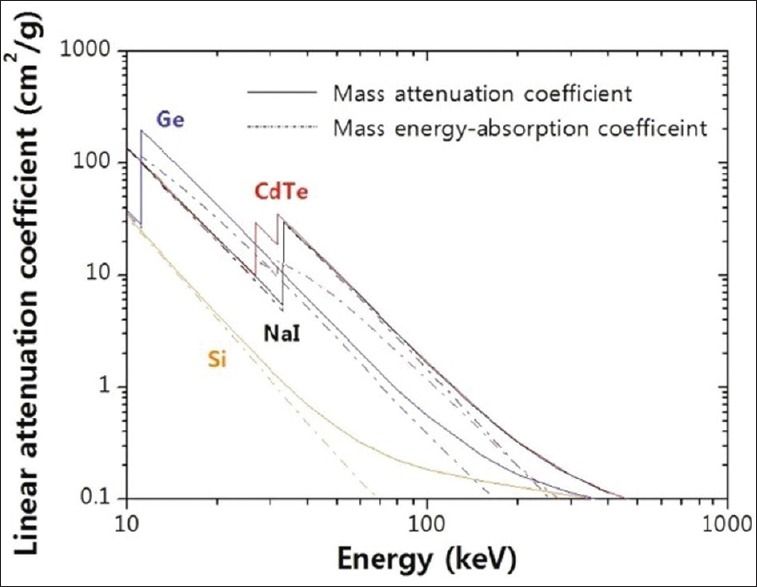
Linear attenuation coeffcients of cadmium telluride, thallium-activated sodium iodide, germanium, and silicon materials. The dashed lines are results for the mass energy-absorption coefficient. Cadmium telluride has a higher photoelectric attenuation coeffcient than do the other materials (used with permission from the author)
Figure 2.
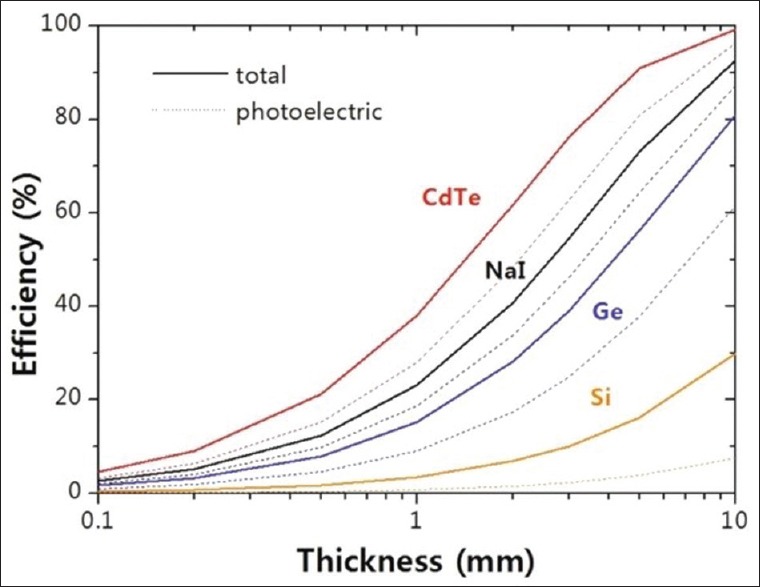
Detection effciency for 140-keV gamma rays for various thicknesses of cadmium telluride, thallium-activated sodium iodide, germanium, and silicon detectors. The drawn lines are results for the total detection effciency; the dashed lines are results for the photoelectric detection effciency (used with permission from the author)
Figure 3.
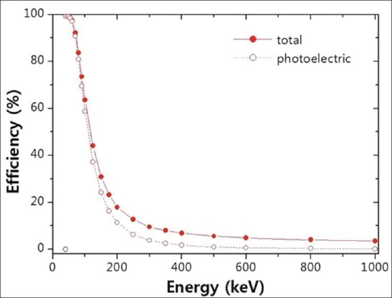
(color online) Detection effciency of the cadmium telluride pixelated semiconductor detector at different energies; the dashed lines are results for the photoelectric detection effciency (used with permission from the author)
While energy resolution of NaI(Tl) was determined approximately 9% full width at half maximum (FWHM) at 140 KeV, it was reported about 4%; hence, the detectors could be simply pixelated and read out straightly.[2,9,27,35] Having a high intrinsic sensitivity reduces the detector thickness for obtaining suitable sensitivity and subsequently improves the spatial resolution.[27] Park et al. evaluated the quality of reconstructed images from CdTe and NaI(Tl) detectors in a small animal SPECT imaging system. The spatial resolution of the detectors was found 2.27 mm and 3.21 mm FWHM, respectively.[7] Meanwhile, a thickness of 5 mm was needed for CdTe to stopping power of 75% with 99mTc at 140 KeV.[13] Jambi et al. have studied the function of the XRI-UNO CdTe detectors and found that the XRI-UNO had acceptable performance for energies lower than 30 KeV, and partly thin CdTe layer could not be proper for imaging with energetic radionuclides.[19]
A main problem of CdTe detectors is polarization effect, which is related to every variations in function of the detector under the biasing condition.[17,26,27,33] The polarization makes difficult maintaining the performances of CdTe detectors without some depolarization methods in high temperature conditions. The technique of periodical turning off the bias voltage has been developed to depolarize the detector (called “refreshing”). The other drawbacks include higher cost and operational complexity. Thus, CdTe is appealing for gamma-ray detection applications.[2]
Radiation Interaction in Semiconductor
Perceiving the charge transport procedure is basic in the improvement of semiconductor detectors.[31] Figure 4 shows a typical planar semiconductor detector schema with metal electrodes on the opposite faces.[17] When a photon interacts with a biased semiconductor, one or more high-energy electrons were created following photoelectric and Compton interactions.[1,36] Through the operative external electric field lines made by the bias voltage, charge flow was created in the sensitive volume and moved in opposite directions toward the electrodes and lead to a transient circuit signal. The electrons loss their energies by two processes: ionization and photon creation. Semiconductor detector acts like an ionization chamber. In the detector, the electron-hole pair is generated instead of the electron-ion pair in the gas detector. Electrons and holes, as negative and positive charges, drift to the anode and cathode electrodes, respectively.[2,3,6,37] In a semiconductor, valence band was filled and conduction band was empty and the space between the bands is band gap. Valence band abandoned when the electrons excited into the conduction band, and hence, a hole was created in valence band e. If E and w define the photon energy and average pair creation energy, respectively, the number of electron-hole pairs (N) will be E/w. Due to defects and impurities in the detector, charge carrier transport features are different between the electrons and the holes. These characteristics are weak in holes and make both their mobility (μh) and lifetime (τh) lower than electrons (μe,τe). Thus, the detector thickness must be measured less than μhτhE which limits the maximum thickness and energy range of the detector; therefore, usual operation of semiconductor detectors is based on the collection efficiency of the charges generated by photon interactions.[1,2,17,22,24,25]
Figure 4.
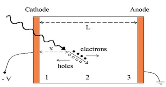
Planar configuration of a semiconductor detector. Electron-hole pairs, generated by radiation, are swept toward the appropriate electrode by the electric field (used with permission from the author)
Medical Imaging with Cadmium Telluride Detector
CdTe semiconductor is the most probable detector for medical imaging devices.[33,38] Applications of CdTe detectors in nuclear medicine were investigated by Scheiber in 2000.[18] CdTe sensors, as X and gamma-ray spectrometers, are really comparable with traditional systems on the basis of solid scintillators, Si and Ge detectors. The main applications of these detectors have defined for gamma cameras with small field of views that may be applied as appropriate small-organ imaging systems such as cardiac, breast, and brain imaging, sentinel lymph node intraoperative mapping, thyroid or parathyroid, and small animal imaging.[1,16,19,39] Furthermore, the CdTe semiconductor detector was developed for simultaneous dual-radioisotopes imaging in SPECT and positron emission tomography. The imaging of dual-radioisotopes will provide two functional images without time difference and position error by a single scan.[30,31,32,33,34,35,36,37,38,39,40,41,42] The planar images of a brain phantom from both CdTe and NaI(Tl) detectors are demonstrated in in Figure 5.[20] The images from CdTe detector have higher contrast and sharpness due to well scatter rejection.[20] CdTe was also used in digital radiography, digital mammography, dental digital radiography, boron neutron capture therapy (BNCT-SPECT), bone densitometry, chest X-ray imaging, electronic portal imaging systems, tomography, computed tomography, and astronomy.[17,19,26,31,33,43,44] Moreover, these detectors can be used as nuclear probes that measure blood flow, evaluation of renal function, pathophysiological cardiac conditions or ambulatory situations, and in the identification of small amounts of tissues (malignant) in the radio-guided surgery such as melanoma and breast cancer.[35]
Figure 5.
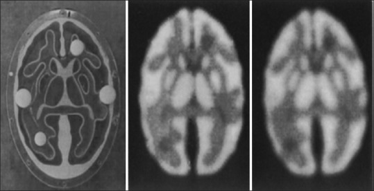
N-isopropyl-p-[123I] Iodoamphetamine (IMP) of brain phantom (a), planar image by cadmium telluride detector module (b) and by anger-type (c), the distance from the phantom surface to collimator surface was 50 mm. The image of cadmium telluride detector (b) is superior in contrast and sharpness than of anger-type (used with permission from the author)
Epitaxial Growth Methods for Cadmium Telluride Detectors
In the recent decade, several epitaxial growth methods were established for thick or thin deposition of the CdTe detectors. To optimize the electrical characteristics and to miniaturize a diverse heterogeneity of CdTe crystals,[17,45] a thick detector deposition was introduced,[17] so that the detector function has highly improved.[46]-Meanwhile, a proper epitaxial growth technique for providing single crystalline thick fil with the following properties was used: (1) a growth rate ranged from 1 to about 100 μm/h; (2) uniformity formation and steady temperature growth, to make homogeneity and perfectly, freeness from defects that would strictly decline the device's performance; (3) the source materials shall be economical in the market.[47] The growth of a flat crystal with a large area has already been a challenging job.[48] The epitaxial growth of a thick CdTe layer on great-area substrates, for instance, GaAs or Si, is a favorable way to provide the large-area detectors.[48,49] Consequently, the Si substrate is better than the GaAs substrates for improving detector performance and attaining an even larger area. However, there is some limitation for the effective growth of epitaxial layers with superior crystalline quality including a great diversity in the thermal expansion coefficients of Si and CdTe, their great lattice-stable inconformity, and the valence mismatch. Typically, the grown layers show poor substrate connection. To keep the uniformity growth on Si substrates, Niraula et al. heated the substrates in a separate chamber with environment hydrogen together with fragments of GaAs at 800°C–900°C.[49] One of the epitaxial growth methods of CdTe on Si substrates is metalorganic vapor phase epitaxy (MOVPE) which is an important method in creating a large area, with high growth rate and a well homogeneity. Therefore, the detector properties by employing thicker CdTe with thickness up to 100 μm film with low dark current were improved. The use of higher bias voltage by MOVPE method which related to decrease the electronic noise develops the collection efficiency. The main problem of the method is to optimize the thickness of the grown crystals accordingly to get good detection efficiency.[13,45,46,48,49,50,51] Traveling heater method (THM) constructed the best spectrometric class of polycrystalline detectors.[52] It could be reduced hole trapping, but two main drawbacks including a small size detector and high leakage current restricted its employment field.[10] Another technique is vertical Bridgman method that creates large volume and area of the detector and deduces the hole trapping.[13,31] Besides, high-pressure Bridgman method, advanced by Digirad and eV-Products, incorporates the high transfer properties of THM grown substrate and the great volume and area of BM method. This method was considered as an important step in achieving high resistance and low price CdTe detector, but mobility lifetime of the holes was poor.[10,13,31,33] Furthermore, close space sublimation (CSS) method is both relatively inexpensive and able to large deposition rates. Accordingly, it is widely applied in preparing polycrystalline CdTe by growing thick single crystal CdTe layer on GaAs and Ge substrate for high energy radiation detectors in solar cells. Jiang et al. showed that CSS is economical, with a high qualified growth, and as a responsible epitaxial deposition method.[47] Recent progress in large area requisitions of CdTe has shifted this photoconductor to the boundary of thin-film fabricating.[51] The thin-film deposition method derives from that CdTe detector utilizes platinum or indium thin films to creates an ohmic contact (photoconductive) or a Schottky diode (blocking contact), respectively.[6,28,53] CdTe detector with an ohmic contact showed an established response over long times and reasonable energy resolution, while CdTe detector with Schottky contact provided higher count rate capabilities and energy resolution. For Schottky CdTe detector, soon after using the detector bias voltage, the energy resolution, sensitivity, and photopeak channel decrease, and the procedures persist for some hours after the start of functioning, so-called polarization phenomenon. Moreover, this effect manipulates the electric field profile and the space-charge distribution in the detector and also imposes a reduction in the thickness of the space charge carrier in a semiconductor detector. To overcome this effect, it proposed periodic switching of the bias in low temperature (−25°C to −20°C).[17,26,27,33,35] Development in energy resolution could be gated by constructing PIN diodes forms with the CdTe material. PIN diodes decrease the charge introduction from metallic contacts by application of greater electric fields and provide a better charge collection efficiency. MOVPE growth is an initial technological footstep toward the production of CdTe based on PIN diode gamma/X-ray detectors. However, it needs considerable amounts of costly source materials for extended growth. Meanwhile, appropriate methods for thin-film deposition are commercially possible.[17,45,47,49,51]
Conclusion
CdTe semiconductor detector has generally some preferences to the scintillator in energy resolution, spatial resolution, sensitivity, and detection efficiency. As a whole, a high quantum efficiency and a high-energy resolution suggest the CdTe semiconductor in comparison with the conventional detector, NaI(Tl), as an appropriate candidate for detection of photons in range of 10–500 KeV, which leads to an improved quality of the images in the imaging system.
Financial support and sponsorship
Nil.
Conflicts of interest
There are no conflicts of interest.
References
- 1.Peterson TE, Furenlid LR. SPECT detectors: The Anger camera and beyond. Phys Med Biol. 2011;56:R145–82. doi: 10.1088/0031-9155/56/17/R01. [DOI] [PMC free article] [PubMed] [Google Scholar]
- 2.Milbrath BD, Peurrung AJ, Bliss M, Weber WJ. Radiation detector materials: An overview. J Mater Res. 2008;23:2561–81. [Google Scholar]
- 3.Heller S, Zanzonico P. Nuclear probes and intraoperative gamma cameras. Semin Nucl Med. 2011;41:166–81. doi: 10.1053/j.semnuclmed.2010.12.004. [DOI] [PubMed] [Google Scholar]
- 4.Weber MJ. Inorganic scintillators: Today and tomorrow. J Lumin. 2002;100:35–45. [Google Scholar]
- 5.Khoshakhlagh M, Islamian JP, Abedi SM, Mahmoudian B. Development of scintillators in nuclear medicine. World J Nucl Med. 2015;14:156–9. doi: 10.4103/1450-1147.163241. [DOI] [PMC free article] [PubMed] [Google Scholar]
- 6.Russo P, Del Guerra A. Solid-state detectors for small-animal imaging. In: Zaidi H, editor. Molecular Imaging of Small Animals: Instrumantation and Aplications. New York: Springer; 2014. pp. 23–82. [Google Scholar]
- 7.Park SJ, Lee CL, Cho HM, Kim HJ. Ultra high resolution SPECT with CdTe for small animal imaging applications: Monte Carlo simulation study using voxelized phantom. J Korean Phys Soc. 2012;60:1145–9. [Google Scholar]
- 8.Ryu HJ, Lee YJ, Lee SW, Cho HM, Choi YN, Kim HJ. Design of a high-resolution small-animal SPECT-CT system sharing a CdTe semiconductor detector. J Korean Phys Soc. 2012;61:130–4. [Google Scholar]
- 9.Lopes M, Chepel V. Detectors for medical radioisotope imaging: Demands and perspectives. Radiat Phys Chem. 2004;71:683–92. [Google Scholar]
- 10.Limousin O. New trends in CdTe and CdZnTe detectors for X-and gamma-ray applications. Nucl Instrum Methods Phys Res. 2003;504:24–37. [Google Scholar]
- 11.Lee YJ, Kim DH, Kim HJ. The effect of high-resolution parallel-hole collimator materials with a pixelated semiconductor SPECT system at equivalent sensitivities: Monte Carlo simulation studies. J Korean Phys Soc. 2014;64:1055–62. [Google Scholar]
- 12.Liu B, Shi C. Development of medical scintillator. Chin Sci Bull. 2002;47:1057–63. [Google Scholar]
- 13.Verger L, Boitel M, Gentet M, Hamelin R, Mestais C, Mongellaz F, et al. Characterization of CdTe and CdZnTe detectors for gamma-ray imaging applications. Nucl Instrum Methods Phys Res. 2001;458:297–309. [Google Scholar]
- 14.Hirano Y, Zeniya T, Iida H. Monte Carlo simulation of scintillation photons for the design of a high-resolution SPECT detector dedicated to human brain. Ann Nucl Med. 2012;26:214–21. doi: 10.1007/s12149-011-0561-4. [DOI] [PubMed] [Google Scholar]
- 15.Madsen MT. Recent advances in SPECT imaging. J Nucl Med. 2007;48:661–73. doi: 10.2967/jnumed.106.032680. [DOI] [PubMed] [Google Scholar]
- 16.Russo P, Mettivier G, Pani R, Pellegrini R, Cinti MN, Bennati P. Imaging performance comparison between a LaBr3: Ce scintillator based and a CdTe semiconductor based photon counting compact gamma camera. Med Phys. 2009;36:1298–317. doi: 10.1118/1.3081412. [DOI] [PubMed] [Google Scholar]
- 17.Del Sordo S, Abbene L, Caroli E, Mancini AM, Zappettini A, Ubertini P. Progress in the development of CdTe and CdZnTe semiconductor radiation detectors for astrophysical and medical applications. Sensors. 2009;9:3491–526. doi: 10.3390/s90503491. [DOI] [PMC free article] [PubMed] [Google Scholar]
- 18.Scheiber C. CdTe and CdZnTe detectors in nuclear medicine. Nucl Instr Meth Phys Res. 2000;448:513–24. [Google Scholar]
- 19.Jambi LK, Lees JE, Bugby S, Tipper S, Alqahtani M, Perkins A. Evaluation of XRI-UNO CdTe detector for nuclear medical imaging. J Instrum. 2015;10:P06012. [Google Scholar]
- 20.Mori I, Takayama T, Motomura N. The CdTe detector module and its imaging performance. Ann Nucl Med. 2001;15:487–94. doi: 10.1007/BF02988500. [DOI] [PubMed] [Google Scholar]
- 21.Lee YJ, Ryu HJ, Cho HM, Lee SW, Choi YN, Kim HJ. Optimization of a high-resolution collimator for a CdTe detector: Monte Carlo simulation studies. J Korean Phys Soc. 2012;60:862–8. [Google Scholar]
- 22.Rizzi M, D'Aloia M, Castagnolo B. Semiconductor detectors and principles of radiation-matter interaction. J Appl Sci. 2010;10:3141–55. [Google Scholar]
- 23.Obrenović MD, Lazarević DR, Stanković SJ, Kartalović NM. The impact of radiation on semiconducting characteristics of monocrystalline silicon and germanium. Nucl Technol Radiat. 2016;31:97–101. [Google Scholar]
- 24.Takahashi T, Watanabe S, Kouda M, Sato G, Okada Y, Kubo S, et al. High-resolution CdTe detector and applications to imaging devices. IEEE Trans Nucl Sci. 2001;48:287–91. [Google Scholar]
- 25.Szeles C. CdZnTe and CdTe materials for X-ray and gamma ray radiation detector applications. Phys Status Solidi B. 2004;241:783–90. [Google Scholar]
- 26.Kubo N, Zhao S, Fujiki Y, Kinda A, Motomura N, Katoh C, et al. Evaluating performance of a pixel array semiconductor SPECT system for small animal imaging. Ann Nucl Med. 2005;19:633–9. doi: 10.1007/BF02985059. [DOI] [PubMed] [Google Scholar]
- 27.Ogawa K, Ohmura N, Iida H, Nakamura K, Nakahara T, Kubo A. Development of an ultra-high resolution SPECT system with a CdTe semiconductor detector. Ann Nucl Med. 2009;23:763–70. doi: 10.1007/s12149-009-0293-x. [DOI] [PubMed] [Google Scholar]
- 28.Andjelkovi MS, Risti GS. Feasibility Study of a current mode gamma radiation dosimeter based on a commercial PIN photodiode and a custom made auto-ranging electrometer. Nucl Technol Radiat. 2013;28:73–83. [Google Scholar]
- 29.Iida H, Ogawa K. Comparison of a pixelated semiconductor detector and a non-pixelated scintillation detector in pinhole SPECT system for small animal study. Ann Nucl Med. 2011;25:143–50. doi: 10.1007/s12149-010-0441-3. [DOI] [PubMed] [Google Scholar]
- 30.Ko T, Utanohara Y, Suzuki Y, Kurihara M, Iguchi N, Umemura J, et al. A preliminary feasibility study of simultaneous dual-isotope imaging with a solid-state dedicated cardiac camera for evaluating myocardial perfusion and fatty acid metabolism. Heart Vessels. 2016;31:38–45. doi: 10.1007/s00380-014-0578-4. [DOI] [PubMed] [Google Scholar]
- 31.Verger L, Bonnefoy JP, Glasser F, Ouvrier-Buffet P. New developments in CdTe and CdZnTe detectors for X and γ-ray applications. J Electron Mater. 1997;26:738–44. [Google Scholar]
- 32.Lee YJ, Ryu HJ, Cho HM, Lee SW, Choi YN, Kim HJ. Optimization of an ultra-high-resolution parallel-hole collimator for CdTe semiconductor SPECT system. J Instrum. 2013;8:C01044. [Google Scholar]
- 33.Scheiber C, Giakos GC. Medical applications of CdTe and CdZnTe detectors. Nucl Instr Meth Phys Res. 2001;458:12–25. [Google Scholar]
- 34.Alruhaili A, Sellin P, Lohstroh A, Boothman V, Veeramani P, Veale M, et al. Development of a CZT drift ring detector for X and X-ray spectroscopy. J Instrum. 2015;10:P04005. [Google Scholar]
- 35.Tsuchimochi M, Sakahara H, Hayama K, Funaki M, Ohno R, Shirahata T, et al. A prototype small CdTe gamma camera for radioguided surgery and other imaging applications. Eur J Nucl Med Mol Imaging. 2003;30:1605–14. doi: 10.1007/s00259-003-1301-3. [DOI] [PubMed] [Google Scholar]
- 36.Nikoli DS, Aleksandra I, Lazarevi DR. Improvement possibilities of the IV characteristics of PIN photodiodes damaged by gamma irradiation. Nucl Technol Radiat. 2013;28:84–91. [Google Scholar]
- 37.Cavallini A, Fraboni B, Dusi W, Auricchio N, Chirco P, Zanarini M, et al. Behavior of CdTe and CdZnTe detectors following electron irradiation. IEEE Trans Nucl Sci. 2002;49:1598–602. [Google Scholar]
- 38.Ogawa K, Muraishi M. Feasibility study on an ultra-high-resolution SPECT with CdTe detectors. IEEE Trans Nucl Sci. 2010;57:17–24. [Google Scholar]
- 39.Suzuki A, Takeuchi W, Ishitsu T, Tsuchiya K, Morimoto Y, Ueno Y, et al. High-sensitivity brain SPECT system using cadmium telluride (CdTe) semiconductor detector and 4-pixel matched collimator. Phys Med Biol. 2013;58:7715–31. doi: 10.1088/0031-9155/58/21/7715. [DOI] [PubMed] [Google Scholar]
- 40.Suzuki A, Takeuchi W, Ueno Y, Kobashi K, Toyonaga T, Shiga T, et al. Monte Carlo-based scatter correction considering the tailing effect of a CdTe detector for dual-isotope brain SPECT imaging. Biomed Phys Eng Express. 2016;2:45010. [Google Scholar]
- 41.Takeuchi W, Suzuki A, Shiga T, Kubo N, Morimoto Y, Ueno Y, et al. Simultaneous Tc-99m and I-123 dual-radionuclide imaging with a solid-state detector-based brain-SPECT system and energy-based scatter correction. EJNMMI Phys. 2016;3:1–18. doi: 10.1186/s40658-016-0147-2. [DOI] [PMC free article] [PubMed] [Google Scholar]
- 42.Takahashi Y, Miyagawa M, Nishiyama Y, Kawaguchi N, Ishimura H, Mochizuki T. Dual radioisotopes simultaneous SPECT of (99m)Tc-tetrofosmin and (123)I-BMIPP using a semiconductor detector. Asia Ocean J Nucl Med Biol. 2015;3:43–9. [PMC free article] [PubMed] [Google Scholar]
- 43.Murata I, Nakamura S, Manabe M, Miyamaru H, Kato I. Characterization measurement of a thick CdTe detector for BNCT-SPECT – Detection efficiency and energy resolution. Appl Radiat Isot. 2014;88:129–33. doi: 10.1016/j.apradiso.2014.01.023. [DOI] [PubMed] [Google Scholar]
- 44.Barber WC, Wessel JC, Nygard E, Iwanczyk JS. Energy dispersive CdTe and CdZnTe detectors for spectral clinical CT and NDT applications. Nucl Instrum Methods Phys Res A. 2015;784:531–7. doi: 10.1016/j.nima.2014.10.079. [DOI] [PMC free article] [PubMed] [Google Scholar]
- 45.Niraula M, Yasuda K, Nakanishi Y, Uchida K, Mabuchi T, Agata Y, et al. Growth of thick CdTe epilayers on GaAs substrates and evaluation of CdTe/n+ -GaAs heterojunction diodes for an X-ray imaging detector. J Electron Mater. 2004;33:645–50. [Google Scholar]
- 46.Yasuda K, Niraula M, Fujimura N, Tachi T, Inuzuka H, Namba S, et al. Dark current characteristics of a radiation detector array developed using MOVPE-grown thick CdTe layers on Si substrate. J Electron Mater. 2012;41:2754–8. [Google Scholar]
- 47.Jiang Q, Brinkman A, Cantwell B, Mullins J, Dierre F, Basu A, et al. Growth of thick epitaxial CdTe films by close space sublimation. J Electron Mater. 2009;38:1548–53. [Google Scholar]
- 48.Niraula M, Yasuda K, Takagi K, Kusama H, Tominaga M, Yamamoto Y, et al. Development of nuclear radiation detectors based on epitaxially grown thick CdTe layers on n+ -GaAs substrates. J Electron Mater. 2005;34:815–9. [Google Scholar]
- 49.Niraula M, Yasuda K, Ohnishi H, Takahashi H, Eguchi K, Noda K, et al. Direct growth of high-quality thick CdTe epilayers on Si (211) substrates by metalorganic vapor phase epitaxy for nuclear radiation detection and imaging. J Electron Mater. 2006;35:1257–61. [Google Scholar]
- 50.Yasuda K, Niraula M, Wajima Y, Yamashita H, Takai N, Suzuki Y, et al. Development of nuclear radiation detectors by use of thick single-crystal CdTe layers grown on (211) p+ -Si substrates by MOVPE. J Electron Mater. 2014;43:2860–3. [Google Scholar]
- 51.Shvydka D, Jin X, Parsai EI. Performance of large area thin-film CdTe detector in diagnostic X-ray imaging. Int J Med Phys Clin Eng Radiat Oncol. 2013;2:98–109. [Google Scholar]
- 52.Peterson JH, Fiederle M, Derby JJ. Analysis of the traveling heater method for the growth of cadmium telluride. J Cryst Growth. 2016;454:45–58. [Google Scholar]
- 53.Tsuchiya K, Takahashi I, Kawaguchi T, Yokoi K, Morimoto Y, Ishitsu T, et al. Basic performance and stability of a CdTe solid-state detector panel. Ann Nucl Med. 2010;24:301–11. doi: 10.1007/s12149-010-0354-1. [DOI] [PubMed] [Google Scholar]