

Abstract

Bifunctional active regions, capable of light generation and detection at the same wavelength, allow a straightforward realization of the integrated mid-infrared photonics for sensing applications. Here, we present a high performance bifunctional device for 8 μm capable of 1 W single facet continuous wave emission at 15 °C. Apart from the general performance benefits, this enables sensing techniques which rely on continuous wave operation, for example, heterodyne detection, to be realized within a monolithic platform and demonstrates that bifunctional operation can be realized at longer wavelength, where wavelength matching becomes increasingly difficult and that the price to be paid in terms of performance is negligible. In laser operation, the device has the same or higher efficiency compared to the best lattice-matched QCLs without same wavelength detection capability, which is only 30% below the record achieved with strained material at this wavelength.
Keywords: quantum cascade laser, quantum cascade detector, lab-on-a-chip, monolithic integrated photonics
Integrated photonics is a growing research field and is often connected to silicon photonics at telecommunication wavelength,1 aiming for high speed optical data links or quantum computing.2,3 However, integrated photonics enables a much wider field of fascinating applications, for example, the realization of extremely compact chemical sensing systems. Active optical devices are mostly realized with epitaxial grown III–V materials, which makes their integration on Si particularly difficult. Heterogeneous integration using transfer techniques allows both single device and wafer scale transfers and were utilized to demonstrate III–V lasers4 and particularly quantum cascade lasers5 integrated on silicon. Also, direct growth of III–Vs on silicon is an active research field with some interesting recent results, for example, the direct growth of a III–V quantum dot laser on a silcon substrate.1 However, the growth of high quality materials will remain challenging. For many applications, the integration of electronics is not particularly important, and III–V substrate-based integration would be sufficient. This allows direct high quality growth without the need for wafer bonding and significantly reduces the packaging costs. An epilayer material which can be used both as a gain as well as a photodetecting medium depending on the applied bias, thereby, serves as an ideal solution for photonic integration. Such a bifunctional active medium provides all the features needed to build lasers, detectors as well as modulators.
Moving to longer wavelength, for example, the mid-infrared fingerprint region, active optical components, such as lasers and detectors, are increasingly difficult to realize, especially when aiming for room-temperature operation. The mid-infrared region is particularly useful, as no other wavelength region can offer the same sensitivity or selectivity for chemical spectroscopy. It even enables selective detection of different isotopes.6 The first developments on molecular beam epitaxy by Cho and Arthur7 and the demonstration of the quantum cascade laser (QCL) by Faist et al.8 significantly pushed the entire field.9,10 QCL-based spectroscopy was pioneered by several groups who earlier identified its high potential to realize sensing setups with a smaller footprint.11−15 Nowadays, QCLs are commercially available and can be found in a number of different applications.
The capability of quantum cascade structures for photodetection16−18 received much less attention, maybe because of the rapid developments of competing technologies, such as MCT detectors19 and photoconductive quantum well infrared detectors.20 However, the ability of using similar device structures and the same materials to realize lasers or detectors led to the proposal that such structures can potentially be used to realize monolithically integrated devices that serve as a single chip solution for chemical sensing.21 The idea is simple, a bifunctional quantum cascade epilayer, which can be used both as a gain as well as photodetection material, serves as a basic building block. Lasers and detector are then realized by patterning this epilayer which covers the entire chip. Finally, together with passive optical elements, a monolithic platform that includes all required optical elements can be realized to downscale mid-infrared laser-based sensor systems to a single chip. The realization of such bifunctional devices requires careful band engineering to allow lasing and detection at the same wavelength and further with a decent performance. The first realization in 2012 required a compromise to be taken in terms of a reduced laser performance.22 The demonstration of a monolithically integrated sensor using plasmonic waveguide demonstrated that such bifunctional active regions allow a straightforward realization of integrated photonics.23 More recently, bifunctional active regions have also been used in prototype gas sensing setups aiming for remote sensing.24,25 Their practical realization is still strongly limited by the device performance and would greatly benefit from continuous wave operation which enables heterodyne detection schemes.
In this paper, we present significant progress on bifunctional device developments to address remaining challenges. First, the presented device is designed for a wavelength of 8 μm to demonstrate that a bifunctional high performance device can also be realized at longer wavelength, where wavelength matching between the laser and the detector becomes increasingly difficult. Thereby, we show that the flexibility due to the engineerable wavelength known from QCLs to address a variety of different sensing applications also applies to bifunctional devices. Second, we pushed the laser performance to a new level, where our bifunctional device can compete or even outperform conventional QCLs. The device is capable of emitting 1 W single facet output power in continuous wave at 15 °C. The achieved wallplug efficiency (WPE) of 12% and 7% in pulsed and continuous wave operation is the equal to or higher than reported values for unstrained material. This clearly shows, that the cost of laser performance due to the additional detection functionality can be negligible.
Design Considerations
Continuous wave operation requires two main ingredients: A temperature insensitive gain medium with a low threshold and a low loss waveguide with a low thermal resistance. The first QCL capable of room-temperature continuous wave emission was demonstrated in 2001 by Beck et al.27 Since then, the output power and wall-plug efficiency have been significantly improved and watt-level output powers are not unusual anymore.28−30 For bifunctional devices the conventional QCL design is modified, such that at zero bias the active transitions can also be used for photodetection at the laser emission wavelength.22 Traditional laser designs, however, show a large spectral shift because the optical transition takes place between the extraction states and the upper laser level. In the first bifunctional designs, wavelength matching was achieved using thicker barriers and reduced energy splittings between the extraction levels, but with the drawback of a reduced laser performance. These devices showed relatively high threshold currents and were restricted to short pulse operation. The introduction of the horizontal-vertical extraction scheme was a significant step to improve the pulsed laser performance.31 As indicated by the name, the extraction from the lower laser level is split into two logical parts. The first part (horizontal extractor) uses 2–3 thick barriers and a reduced coupling to maintain wavelength matching between the laser and the detector. The second part (vertical extractor) uses multiple strongly coupled states to achieve fast LO-phonon scattering and to prevent thermal backfilling, described in more detail in ref (31). The presented device is designed for 8 μm to show that wavelength matching can also be achieved at longer wavelengths. There, the intrinsic wavelength shift, which should be compensated, becomes more and more pronounced and makes wavelength matching more difficult. This is because the ratio between the photon energy and the splitting between the extraction states, which is usually matched to the LO-phonon energy, increases. Here, we show, that wavelength matching is still possible with the horizontal-vertical extractor design procedure, although we take a small compromise. To maximize the overall performance we accepted a small remaining detuning between the laser spectrum and the peak photoresponse, which slightly reduces the responsivity at the emission wavelength, but allows a better laser performance.
In order to push the device performance to enable a low threshold at high temperatures, we reworked the second part of the injector to achieve an even lower thermal backfilling and more efficient injection. In the literature, the band diagram of a QCL is commonly plotted for one bias. However, it has to be noted that during the design process it is required to take care of the entire bias region from zero to roll-over to identify undesired current paths and regions of negative differential resistance. Furthermore, aiming for continuous wave operation (in contrast to pulsed operation), it is not particularly useful to optimize the device at the bias where the injector state is aligned with the upper laser level. This situation occurs at the roll-over in pulsed mode, which is above the thermal roll-over in continuous wave. More important for continuous wave operation is to achieve a low laser threshold at high operation temperatures. Thus, we mainly optimized our device for bias conditions slightly above threshold, while assuming a high electron temperature. To give a better insight, we plot the band diagram of our design for three selected laser conditions (threshold, highest wallplug efficiency in pulsed mode, roll-over in pulsed mode) as well as for the detector operation at zero bias in Figure 1. Graded interfaces were used in the band structure design to model the behavior of the MOVPE growth. Interface grading strongly modifies the banddiagram and leads to a red-shift in experiments. Here, we directly considered the grading in our design process via an empirically determined width from the wavelength shift between experiment and simulation of a number of previously grown devices, which later turned out to be consistent with the profiles obtained from atom probe tomography measurements. This approach allows a reliable prediction of the emission wavelength and a more accurate design. A more detailed description of our interface grading model can be found in refs (32 and 33).
Figure 1.

Band diagram at laser threshold, bias of highest pulsed wallplug efficiency, and rollover, as well as at detector bias (zero bias). Graded interfaces due to MOVPE growth are considered in the model. The dashed line indicates the pocket-shaped injector.26
The injector is designed in such a way that it forms a triangularly shaped effective potential. This approach is similar to the so-called pocket injector design.26 Electrons can scatter down into the pocket and the large energy separation minimizes thermal backfilling. We want to emphasize that at laser threshold, the energy distance between the lowest injector ground state and the upper laser level is quite large (26 meV). However, at room temperature, and keeping in mind that the electron temperature can be much higher than the lattice temperature in this region due to the emission of off-resonant LO-phonons, thermal excitation from the injector to the upper laser level is sufficient to achieve population inversion of the laser transition and provides an additional cooling effect for hot electrons. Thus, a quite large part of the voltage drop through the injector is compensated by the required “cooling” energy to inject electrons into the upper laser level (at threshold 70 meV – 26 meV = 44 meV). The simulation tool used for this work resolves the k-space and thus includes nonequilibrium in-plane distributions.34 The effective potential is continuously tilted with increasing bias as illustrated by the dashed line in the band diagrams (see Figure 1). The ground state thereby moves from the middle to the right to achieve an increasing direct injection. This allows for an efficient lower laser level depopulation over the entire bias range. At the bias where light generation is the most efficient, the upper laser level is still significantly above the lowest ground state (band diagram 2). The roll-over in pulsed mode occurs, when the ground state of the injector is in resonance with the upper laser level (band diagram 3). A further increase in bias would lead to a region of negative differential resistance. Following, domains for different electric field will form in order to maximize current flow and the laser shuts off because of misalignment. A main difference to an injector with one pronounced tunneling level is that the injection current is mainly limited by thermal excitation of hot electrons rather than the tunneling efficiency. The single tunneling level injector does not allow for large cooling effects but might require a slightly smaller doping density. However, it is not obviously clear if a slightly higher doping results in higher loss, as the conventional Drude absorption model for bulk collapses for subband devices. Free-carrier absorption in quantum cascade structures is fundamentally different and becomes very small.35 The reduction of the lower laser level population can be expected to give a larger contribution.
The second ingredient for continuous wave operation is a low loss waveguide with a low thermal resistance. This is a main reason, why the highest performance levels where mostly achieved using material systems on InP substrates.28−30 InP is an ideal cladding material with low optical loss and high thermal conductivity. In contrast to previous devices we used low doped InP top and bottom cladding layers as well as lateral InP regrowth for better heat extraction.36 The low optical loss of this waveguide allows a reduction of the active region doping by roughly a factor of 2 compared to previous bifunctional devices to further reduce the laser threshold.
Growth and Fabrication
The QCLD, designed for 8 μm, was grown nominally lattice matched on n-InP (2.5 × 1018 cm–3) substrates by MOVPE in a Veeco D125 multiwafer reactor. The layer structure of the QCLD is as follows, with InAlAs barriers in bold: 3.5 μm InP (3 × 1016 cm–3); bottom contact chirped superlattice: 1.2, 2.2, 2.0, 2.4, 2.0, 2.6, 2.0, 2.8, 1.8, 3.0, 1.6, 3.2, 1.5, 3.5, 1.4, 4.0, 1.2, 4.5, 1.1, 5.0, 1.0 nm (all layers doped 4 × 1016 cm–3); 200 nm InGaAs (4 × 1016 cm–3); bottom contact charge-balancing region: 2.5, 6.0, 2.5, 5.5,2.5 nm (underlined layers doped 2 × 1017 cm–3); 35× active region: 5.5, 2.1, 6.7, 1.1, 1.9, 3.9, 2.9, 2.3, 2.95, 2.4, 3.3, 2.0, 3.6, 1.9, 3.8, 1.8, 4.0, 1.7, 4.2, 1.7, 4.6, 2.2 (underlined layers doped 9 × 1016 cm–3); top contact charge-balancing region: 5.5, 2.1 (both layers doped 3 × 1017 cm–3); 200 nm InGaAs (4 × 1016 cm–3); top contact superlattice (reverse of bottom contact chirped superlattice); 3.5 μm InP (3 × 1016 cm–3); 700 nm InP (7 × 1018 cm–3); 200 nm InP (1 × 1019 cm–3); 200 nm InGaAs (2.5 × 1019 cm–3). Chirped superlattice and charge-balancing contacts were included to minimize series resistances and to maintain a flat-band condition at zero bias. These regions were carefully designed to prevent unintentional resonant absorption. Please note that the given the active region layer sequence is optimized for the particular MOVPE system by considering interface grading in the bandstructure calculations. The layer sequence has to be modified for growth on different systems, in particular, for molecular beam epitaxy, due to the much sharper interfaces.
The laser ridges were fabricated by conventional photolithography and dry etching. The devices for pulsed measurements and the on-chip detector characterization were fabricated using SiN passivation, sputtered Ti–Au top contacts and were mounted episide up. The continuous wave devices were fabricated in the buried heterostructure configuration using lateral Fe-InP regrowth and with Ti–Au contacts on both sides. The buried heterostructure devices were cleaved to single devices and mounted episide down. The laser performance was characterized with standard equipment, for example, FTIR, pulser, low noise dc current source, and so on. The optical power was measured with a calibrated power meter considering an estimated collection efficiency of 95%, which is consistent with the measurements performed at MIT-LL for this and the QCL of ref (37).
Laser Operation
The improvements in the active region design in combination with the optimized waveguide enable bifunctional device with outstanding laser performance. Figure 2 show the light-current-output power relation for two devices. The episide-up mounted device shows an excellent pulsed performance with a total wallplug efficiencs of 12%. The inset shows the temperature dependence of the threshold current density and slope efficiency, from which we extract the characteristic temperatures T0 = 215 K and T1 = 236 K, respectively. High characteristic temperatures are crucial for high temperature operation. The second sample is a longer buried heterostructure device, which was mounted episide-down on a water cooling block without Peltier element. It is capable to emit 1 W single facet output power in continuous wave at 15 °C cooling water temperature and achieves a maximum wallplug efficiency of 7%. Both the pulsed and continuous wave performance are excellent when compared to record values from literature. Table 1 summarizes published power and efficiency record values for the emission wavelengths around 8 μm. The achieved wallplug efficiencies are just 30% smaller compared to the highest published records at this wavelength. One has to note that these record values were achieved with conventional QCLs without same wavelength detection functionality using strained materials. It has been extensively discussed that strained materials have a significant advantage to realize efficient devices.42,43 Unstrained devices suffer from carrier leakage because of the relatively small band-offset, where in well designed strained devices carrier leakage can be neglected at such long wavelength. Compared to QCLs based on unstrained materials, our device outperforms most published results and performs similar compared to QCLs from the same facility. We have grown several QCLs, designed for emission wavelengths between 7.5 and 9 μm, along with the QCLD to test the graded interface model,32,33 as well as to quantify the performance degradation due to the bifunctional operation. Quantitatively, the difference in performance between the QCLD and QCLs is in the same range as the difference between the QCLs and we can conclude that the QCLD performs similar to the best lasers from our facility.
Figure 2.

Current, voltage, and single facet output power relation, as well as total wall plug efficiency (both facets) for an episide-up mounted device in pulsed operation (upper) and a episide-down mounted buried heterostructure device in continuous wave operation (lower). The inset shows the temperature dependence of the threshold current density and slope efficiency in pulsed operation. From this we extract the characteristic temperatures T0 = 215 K and T1 = 236 K via least-squares fits (solid lines).
Table 1. Table of Selected High Performance Continuous Wave QCLs from Literaturea.
| authors | λ | P | η | T | type |
|---|---|---|---|---|---|
| Maulini et al.38 | 7.1 μm | 1.4 W (2.9 W) | 10% (19%) | 20 °C | QCL strained |
| Troccoli et al.39 | 9.2 μm | 2 W (4.4 W) | 10% (16%) | 15 °C | QCL strained |
| 7.8 μm | 0.8 W (-) | 3.4% (-) | 15 °C | QCL unstrained | |
| 8.9 μm | 0.92 W (-) | 4.0% (-) | 15 °C | QCL unstrained | |
| Bismuto et al.40 | 8.5 μm | 0.45 W (1.1 W) | - (11.5%) | 20 °C | QCL unstrained |
| Fujita et al.41 | 8.6 μm | 0.313 W (6.5 W) | 2.74% (10.8%) | 30 °C | QCL unstrained |
| Missaggia et al.37 | 9 μm | 1 W (-) | 7% (-) | 15 °C | QCL unstrained (same facility) |
| Schwarz et al.31 | 6.8 μm | - (0.5 W) | - (4.5%) | 20 °C | QCLD unstrained |
| this work | 8 μm | 1 W (1.5 W) | 7% (12%) | 15 °C | QCLD unstrained |
The values in brackets correspond to pulsed operation. The given values for pulsed and continuous wave correspond to the highest values achieved in the respective operation mode and are not necessarily from the same device geometry. Often narrower ridges have been used for continuous wave operation.
The emission spectrum in continuous wave is shown in Figure 3. Starting from single mode at threshold, the spectrum switches very early to the dense mode, where all Fabry–Perot modes are occupied, and we did not observe the harmonic regime.44 This is a hint of a strong four-wave mixing process and low dispersion in this device. At higher currents the spectrum widens to about 80 cm–1. The spectra at the bias of highest WPE is perfectly centered around the design wavelength of 8 μm. This shows, that considering graded interfaces during the design process enables a reliable prediction of the emission wavelength.32
Figure 3.

Emission spectra of the episide-down mounted QCLD in continuous wave operation. The shown spectral evolution is typical to QCLs: At threshold the laser starts at a single mode and then switches to a dense spectrum, where all Fabry-Perót modes laser, with growing bandwidth.
Detector Operation
The detector
functionality of the bifunctional device has a similar performance
compared to previous designs,22,23,31 considering the smaller device resistance, which originates from
its exponential relation to the photon energy via the activation energy.
As pointed out by earlier work, the device resistance is not as crucial
due to the geometrical advantage of the end-fire coupled on-chip detector.31Figure 4 shows the detector spectrum compared to the laser emission
spectrum. As described above, a small remaining wavelength shift was
accepted during design to achieve a better overall performance. Due
to the small facet size, the characterization with external sources
is possible but challenging because it requires precise knowledge
of the beam profile and spectral density to estimate the incident
optical power. Here, we use the on-chip configuration where the laser
and the detector ridges are separated with a small gap45 to obtain the absolute value of the detector
responsivity. This approach requires calibration via the coupling
efficiency from the laser to the detector as well as the laser output
power. These values typically fluctuate much less and can be obtained
using a power meter collecting light from the second laser facet and
3D FEM modeling to obtain the reflectivities and the coupling efficiency.
Furthermore, the on-chip characterization better represents the configuration
used for on-chip sensing applications. Figure 5 shows the signal of the on-chip detector
at the back facet compared to a calibrated external detector at the
front laser facet. The gap between the laser and the detector can
have a strong influence on the laser facet reflectivity. Thus, we
measured the gap size using a scanning electron microscope to be 5.4
μm ± 0.1 μm and calculated the laser facet reflectivity
from the 3D FEM simulation. From this the power ratio between back
and front side laser emission can be calculated to be  . From the 3D FEM simulation
we also obtain the coupling factor from the back facet emission to
the detector (ηcoupling = 0.57 ± 0.015). The
ratio between the power inside the detector and emitted from the front
facet is then r21ηcoupling = 0.53 ± 0.02. As we consider the detector facet to be a part
of the detector, we divide the ratio by the transitivity to obtain
the total correction factor rcorr = r21ηcoupling/(1 – Rdetector) = 0.71 ± 0.027. From this quite
rigorous approach, we can calculate the responsivity of the on-chip
detector at the laser emission wavelength to be R8 μm = Iph/(rcorrPmeas) ≈
14 mA/W and the peak responsivity to be Rpeak ≈ 20 mA/W.
. From the 3D FEM simulation
we also obtain the coupling factor from the back facet emission to
the detector (ηcoupling = 0.57 ± 0.015). The
ratio between the power inside the detector and emitted from the front
facet is then r21ηcoupling = 0.53 ± 0.02. As we consider the detector facet to be a part
of the detector, we divide the ratio by the transitivity to obtain
the total correction factor rcorr = r21ηcoupling/(1 – Rdetector) = 0.71 ± 0.027. From this quite
rigorous approach, we can calculate the responsivity of the on-chip
detector at the laser emission wavelength to be R8 μm = Iph/(rcorrPmeas) ≈
14 mA/W and the peak responsivity to be Rpeak ≈ 20 mA/W.
Figure 4.

Spectral responsivity of the ridge detector and the normalized laser emission spectrum. A small remaining wavelength-shift was accepted during the design to optimize the overall performance.
Figure 5.

Laser pulse measured the on-chip detector and a calibrated external detector. The laser ridge length for this experiment is significantly smaller and results in a reduced output power. The inset shows the 3D FEM simulation result for the coupling trough the 5.4 μm gap.
We measured multiple detectors
with different ridge lengths (50, 100, 200, and 500 μm) to obtain
the absorption coefficient at the laser emission wavelength of α8μm = 60 cm–1. Compared to previous
devices,22,31 the absorption coefficient is lower due
to the reduced doping. However, due to the end-fire coupled waveguide
detector and the fact that also the waveguide losses are much smaller,
the same absorption efficiency can be achieved just by using longer
ridges. We calculate the optimal detector ridge length in terms of
Johnson noise equivalent power at the laser emission wavelength NEP8μmJ to be
200 μm, with 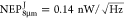 . Longer detectors
are preferable if the noise of the system is limited by other sources.
Here, one can immediately recognize the noise reduction due to the
small size as a major advantage over external discrete detectors,
beside larger coupling and absorption efficiencies. This is a main
reason why the on-chip detector can outperform discrete QCDs although
the resistance-area product is significantly smaller. The optimization
of the resistance is very limited for bifunctional devices, as the
typical strategy of using larger barriers would not allow for laser
operation.
. Longer detectors
are preferable if the noise of the system is limited by other sources.
Here, one can immediately recognize the noise reduction due to the
small size as a major advantage over external discrete detectors,
beside larger coupling and absorption efficiencies. This is a main
reason why the on-chip detector can outperform discrete QCDs although
the resistance-area product is significantly smaller. The optimization
of the resistance is very limited for bifunctional devices, as the
typical strategy of using larger barriers would not allow for laser
operation.
Conclusion and Discussion
With this work we brought bifunctional QCLDs to a new performance level, where in laser operation they can directly compete with conventional QCLs. The on-chip detection feature shows high signal-to-noise ratios due to the coupling scheme and enables a straightforward realization of monolithically integrated mid-infrared sensors. The demonstration of continuous-wave operation at 8 μm is an important step to push integrated sensing systems. It shows that the wavelength scalability known from QCLs also applies for bifunctional designs and enables sensing schemes that rely on continuous wave emission due to the required stability. One of the most interesting and prominent techniques is heterodyne detection, which enables phase sensitive detection of extremely small power levels. This makes heterodyne detection attractive for remote sensing and stand-off detection.46 This concept is particularly useful for on-chip integration as detection of the beating between two laser lines is fundamentally insensitive to electric crosstalk between the lasers and detector and can potentially solve current issues of recently presented gas sensors.24 High power local oscillators can be easily realized and directly coupled to the detectors. Going one step further, the heterodyne detection concept can also be applied in parallel at multiple wavelengths. Using frequency combs, an entire spectrum covering several 10–100 wavenumbers can be acquired with a single shot. Frequency combs have been recently realized using QCL active regions,47,48 which, together with the demonstration of continuous wave bifunctional devices, opens the perspective of on-chip dual comb spectroscopy. Also, for discrete sensing setups, one can switch to lasers based on bifunctional materials, as they show similar performance, but enable integrated power monitoring, stabilization, or referencing.
Acknowledgments
The authors gratefully acknowledge valuable technical discussions on QCL design with Jerome Faist. B.S. and G.S. were supported by the Austrian Science Fund (FWF) within the framework of the Doctoral School Solids4Fun (Project W1243) and the projects NextLite (F4909–N23) and NanoPlas (P28914–N27). The work conducted by Lincoln Laboratory was sponsored by Assistant Secretary of Defense for Research and Engineering (ASD R&E) under Air Force Contract FA8721-05-C-0002. Opinions, interpretations, conclusions, and recommendations are those of the authors and are not necessarily endorsed by the United States Government.
The authors declare no competing financial interest.
References
- Chen S.; Li W.; Wu J.; Jiang Q.; Tang M.; Shutts S.; Elliott S. N.; Sobiesierski A.; Seeds A. J.; Ross I.; Smowton P. M.; Liu H. Electrically pumped continuous-wave III–V quantum dot lasers on silicon. Nat. Photonics 2016, 10, 307–312. 10.1038/nphoton.2016.21. [DOI] [Google Scholar]
- Vivien L.; Pavesi L.. Handbook of silicon photonics; Taylor & Francis, 2016. [Google Scholar]
- Pavesi L.; Lockwood D. J.. Silicon photonics; Springer Science & Business Media, 2004; Vol. 1. [Google Scholar]
- Justice J.; Bower C.; Meitl M.; Mooney M. B.; Gubbins M. A.; Corbett B. Wafer-scale integration of group III–V lasers on silicon using transfer printing of epitaxial layers. Nat. Photonics 2012, 6, 610–614. 10.1038/nphoton.2012.204. [DOI] [Google Scholar]
- Spott A.; Peters J.; Davenport M. L.; Stanton E. J.; Merritt C. D.; Bewley W. W.; Vurgaftman I.; Kim C. S.; Meyer J. R.; Kirch J.; Mawst L. J.; Botez D.; Bowers J. E. Quantum cascade laser on silicon. Optica 2016, 3, 545–551. 10.1364/OPTICA.3.000545. [DOI] [Google Scholar]
- Haas J.; Mizaikoff B. Advances in Mid-Infrared Spectroscopy for Chemical Analysis. Annu. Rev. Anal. Chem. 2016, 9, 45–68. 10.1146/annurev-anchem-071015-041507. [DOI] [PubMed] [Google Scholar]
- Cho A.; Arthur J. Molecular beam epitaxy. Prog. Solid State Chem. 1975, 10, 157–191. 10.1016/0079-6786(75)90005-9. [DOI] [Google Scholar]
- Faist J.; Capasso F.; Sivco D. L.; Sirtori C.; Hutchinson A. L.; Cho A. Y. Quantum Cascade Laser. Science 1994, 264, 553–556. 10.1126/science.264.5158.553. [DOI] [PubMed] [Google Scholar]
- Capasso F. High-performance midinfrared quantum cascade lasers. Opt. Eng. 2010, 49, 111102. 10.1117/1.3505844. [DOI] [Google Scholar]
- Rauter P.; Capasso F. Multi-wavelength quantum cascade laser arrays. Laser Photonics Rev. 2015, 9, 452–477. 10.1002/lpor.201500095. [DOI] [Google Scholar]
- Namjou K.; Cai S.; Whittaker E. A.; Faist J.; Gmachl C.; Capasso F.; Sivco D. L.; Cho A. Y. Sensitive absorption spectroscopy with a room-temperature distributed-feedback quantum-cascade laser. Opt. Lett. 1998, 23, 219–221. 10.1364/OL.23.000219. [DOI] [PubMed] [Google Scholar]
- Kosterev A. A.; Curl R. F.; Tittel F. K.; Gmachl C.; Capasso F.; Sivco D. L.; Baillargeon J. N.; Hutchinson A. L.; Cho A. Y. Methane concentration and isotopic composition measurements with a mid-infrared quantum-cascade laser. Opt. Lett. 1999, 24, 1762–1764. 10.1364/OL.24.001762. [DOI] [PubMed] [Google Scholar]
- Paldus B. A.; Spence T. G.; Zare R. N.; Oomens J.; Harren F. J. M.; Parker D. H.; Gmachl C.; Capasso F.; Sivco D. L.; Baillargeon J. N.; Hutchinson A. L.; Cho A. Y. Photoacoustic spectroscopy using quantum-cascade lasers. Opt. Lett. 1999, 24, 178–180. 10.1364/OL.24.000178. [DOI] [PubMed] [Google Scholar]
- Lendl B.; Frank J.; Schindler R.; Müller A.; Beck M.; Faist J. Mid-Infrared Quantum Cascade Lasers for Flow Injection Analysis. Anal. Chem. 2000, 72, 1645–1648. 10.1021/ac990833b. [DOI] [PubMed] [Google Scholar]
- Gittins C. M.; Wetjen E. T.; Gmachl C.; Capasso F.; Hutchinson A. L.; Sivco D. L.; Baillargeon J. N.; Cho A. Y. Quantitative gas sensing by backscatter-absorption measurements of a pseudorandom code modulated λ ∼ 8-μm quantum cascade laser. Opt. Lett. 2000, 25, 1162–1164. 10.1364/OL.25.001162. [DOI] [PubMed] [Google Scholar]
- Hofstetter D.; Beck M.; Faist J. Quantum-cascade-laser structures as photodetectors. Appl. Phys. Lett. 2002, 81, 2683–2685. 10.1063/1.1512954. [DOI] [Google Scholar]
- Gendron L.; Carras M.; Huynh A.; Ortiz V.; Koeniguer C.; Berger V. Quantum cascade photodetector. Appl. Phys. Lett. 2004, 85, 2824–2826. 10.1063/1.1781731. [DOI] [Google Scholar]
- Reininger P.; Zederbauer T.; Schwarz B.; Detz H.; MacFarland D.; Andrews A. M.; Schrenk W.; Strasser G. InAs/AlAsSb based quantum cascade detector. Appl. Phys. Lett. 2015, 107, 081107. 10.1063/1.4929501. [DOI] [PubMed] [Google Scholar]
- Rogalski A. HgCdTe infrared detector material: history, status and outlook. Rep. Prog. Phys. 2005, 68, 2267–2336. 10.1088/0034-4885/68/10/R01. [DOI] [Google Scholar]
- Schneider H.; Liu H. C.. Quantum Well Infrared Photodetectors; Springer: Berlin, 2006. [Google Scholar]
- Kim S.-S.; Young C.; Mizaikoff B. Miniaturized mid-infrared sensor technologies. Anal. Bioanal. Chem. 2008, 390, 231–237. 10.1007/s00216-007-1673-5. [DOI] [PubMed] [Google Scholar]
- Schwarz B.; Reininger P.; Detz H.; Zederbauer T.; Andrews A. M.; Kalchmair S.; Schrenk W.; Baumgartner O.; Kosina H.; Strasser G. A bi-functional quantum cascade device for same-frequency lasing and detection. Appl. Phys. Lett. 2012, 101, 191109. 10.1063/1.4767128. [DOI] [Google Scholar]
- Schwarz B.; Reininger P.; Ristanić D.; Detz H.; Andrews A. M.; Schrenk W.; Strasser G. Monolithically integrated mid-infrared lab-on-a-chip using plasmonics and quantum cascade structures. Nat. Commun. 2014, 5, n/a. 10.1038/ncomms5085. [DOI] [PMC free article] [PubMed] [Google Scholar]
- Harrer A.; Szedlak R.; Schwarz B.; Moser H.; Zederbauer T.; MacFarland D.; Detz H.; Andrews A. M.; Schrenk W.; Lendl B.; Strasser G. Mid-infrared surface transmitting and detecting quantum cascade device for gas-sensing. Sci. Rep. 2016, 6, 21795. 10.1038/srep21795. [DOI] [PMC free article] [PubMed] [Google Scholar]
- Szedlak R.; Harrer A.; Holzbauer M.; Schwarz B.; Waclawek J. P.; MacFarland D.; Zederbauer T.; Detz H.; Andrews A. M.; Schrenk W.; Lendl B.; Strasser G. Remote Sensing with Commutable Monolithic Laser and Detector. ACS Photonics 2016, 3, 1794–1798. 10.1021/acsphotonics.6b00603. [DOI] [PMC free article] [PubMed] [Google Scholar]
- Bismuto A.; Terazzi R.; Hinkov B.; Beck M.; Faist J. Fully automatized quantum cascade laser design by genetic optimization. Appl. Phys. Lett. 2012, 101, 021103. 10.1063/1.4734389. [DOI] [Google Scholar]
- Beck M. Continuous Wave Operation of a Mid-Infrared Semiconductor Laser at Room Temperature. Science 2002, 295, 301–305. 10.1126/science.1066408. [DOI] [PubMed] [Google Scholar]
- Bai Y.; Bandyopadhyay N.; Tsao S.; Slivken S.; Razeghi M. Room temperature quantum cascade lasers with 27% wall plug efficiency. Appl. Phys. Lett. 2011, 98, 181102. 10.1063/1.3586773. [DOI] [Google Scholar]
- Razeghi M.; Slivken S.; Bai Y.; Gokden B.; Darvish S. R. High power quantum cascade lasers. New J. Phys. 2009, 11, 125017. 10.1088/1367-2630/11/12/125017. [DOI] [Google Scholar]
- Xie F.; Caneau C.; Leblanc H. P.; Caffey D. P.; Hughes L. C.; Day T.; en Zah C. Watt-Level Room Temperature Continuous-Wave Operation of Quantum Cascade Lasers With λ < 10 μm. IEEE J. Sel. Top. Quantum Electron. 2013, 19, 1200407. 10.1109/JSTQE.2013.2240658. [DOI] [Google Scholar]
- Schwarz B.; Ristanic D.; Reininger P.; Zederbauer T.; MacFarland D.; Detz H.; Andrews A. M.; Schrenk W.; Strasser G. High performance bi-functional quantum cascade laser and detector. Appl. Phys. Lett. 2015, 107, 071104. 10.1063/1.4927851. [DOI] [Google Scholar]
- Wang C.; Schwarz B.; Siriani D.; Connors M.; Missaggia L.; Calawa D.; McNulty D.; Akey A.; Zheng M.; Donnelly J.; Mansuripur T.; Capasso F. Sensitivity of heterointerfaces on emission wavelength of quantum cascade lasers. J. Cryst. Growth 2017, 464, 215–220. 10.1016/j.jcrysgro.2016.11.029. [DOI] [Google Scholar]
- Wang C. A.; Schwarz B.; Siriani D. F.; Missaggia L. J.; Connors M. K.; Mansuripur T. S.; Calawa D. R.; McNulty D.; Nickerson M.; Donnelly J. P.; Creedon K.; Capasso F. MOVPE Growth of LWIR AlInAs/GaInAs/InP Quantum Cascade Lasers: Impact of Growth and Material Quality oan Laser Performance. IEEE J. Sel. Top. Quantum Electron. 2017, 1. 10.1109/JSTQE.2017.2677899. [DOI] [Google Scholar]
- Baumgartner O.; Stanojevic Z.; Kosina H. In Monte Carlo Methods and Applications; Sabelfeld K. K., Dimov I., Eds.; De Gruyter Borovets, Bulgaria, 2012; pp 59–67. [Google Scholar]
- Carosella F.; Ndebeka-Bandou C.; Ferreira R.; Dupont E.; Unterrainer K.; Strasser G.; Wacker A.; Bastard G. Free-carrier absorption in quantum cascade structures. Phys. Rev. B: Condens. Matter Mater. Phys. 2012, 85, n/a. 10.1103/PhysRevB.85.085310. [DOI] [Google Scholar]
- Beck M.; Faist J.; Oesterle U.; Ilegems M.; Gini E.; Melchior H. Buried heterostructure quantum cascade lasers with a large optical cavity waveguide. IEEE Photonics Technol. Lett. 2000, 12, 1450–1452. 10.1109/68.887653. [DOI] [Google Scholar]
- Missaggia L.; Wang C.; Connors M.; Saar B.; Sanchez-Rubio A.; Creedon K.; Turner G.; Herzog W. Thermal management of quantum cascade lasers in an individually addressable monolithic array architecture. Proc. SPIE 2016, 9730, 973008. 10.1117/12.2208923. [DOI] [Google Scholar]
- Maulini R.; Lyakh A.; Tsekoun A.; Patel C. K. N. λ ∼ 7.1 μm quantum cascade lasers with 19% wall-plug efficiency at room temperature. Opt. Express 2011, 19, 17203–17211. 10.1364/OE.19.017203. [DOI] [PubMed] [Google Scholar]
- Troccoli M.; Lyakh A.; Fan J.; Wang X.; Maulini R.; Tsekoun A. G.; Go R.; Patel C. K. N. Long-Wave IR Quantum Cascade Lasers for emission in the λ = 8–12μm spectral region. Opt. Mater. Express 2013, 3, 1546–1560. 10.1364/OME.3.001546. [DOI] [Google Scholar]
- Bismuto A.; Terazzi R.; Beck M.; Faist J. Electrically tunable, high performance quantum cascade laser. Appl. Phys. Lett. 2010, 96, 141105. 10.1063/1.3377008. [DOI] [Google Scholar]
- Fujita K.; Furuta S.; Sugiyama A.; Ochiai T.; Edamura T.; Akikusa N.; Yamanishi M.; Kan H. High-Performance λ ∼ 8.6 μm Quantum Cascade Lasers With Single Phonon-Continuum Depopulation Structures. IEEE J. Quantum Electron. 2010, 46, 683–688. 10.1109/JQE.2010.2048015. [DOI] [Google Scholar]
- Faist J.Quantum Cascade Lasers; Oxford University Press, 2013. [Google Scholar]
- Botez D.; Chang C.-C.; Mawst L. J. Temperature sensitivity of the electro-optical characteristics for mid-infrared (λ = 3–16 μm)-emitting quantum cascade lasers. J. Phys. D: Appl. Phys. 2016, 49, 043001. 10.1088/0022-3727/49/4/043001. [DOI] [Google Scholar]
- Mansuripur T. S.; Vernet C.; Chevalier P.; Aoust G.; Schwarz B.; Xie F.; Caneau C.; Lascola K.; en Zah C.; Caffey D. P.; Day T.; Missaggia L. J.; Connors M. K.; Wang C. A.; Belyanin A.; Capasso F. Single-mode instability in standing-wave lasers: The quantum cascade laser as a self-pumped parametric oscillator. Phys. Rev. A: At., Mol., Opt. Phys. 2016, 94, 063807. 10.1103/PhysRevA.94.063807. [DOI] [Google Scholar]
- Schwarz B.; Reininger P.; Detz H.; Zederbauer T.; Andrews A.; Schrenk W.; Strasser G. Monolithically Integrated Mid-Infrared Quantum Cascade Laser and Detector. Sensors 2013, 13, 2196–2205. 10.3390/s130202196. [DOI] [PMC free article] [PubMed] [Google Scholar]
- Wang Y.; Soskind M. G.; Wang W.; Wysocki G. High-resolution multi-heterodyne spectroscopy based on Fabry-Perot quantum cascade lasers. Appl. Phys. Lett. 2014, 104, 031114. 10.1063/1.4862756. [DOI] [Google Scholar]
- Hugi A.; Villares G.; Blaser S.; Liu H. C.; Faist J. Mid-infrared frequency comb based on a quantum cascade laser. Nature 2012, 492, 229–233. 10.1038/nature11620. [DOI] [PubMed] [Google Scholar]
- Villares G.; Hugi A.; Blaser S.; Faist J. Dual-comb spectroscopy based on quantum-cascade-laser frequency combs. Nat. Commun. 2014, 5, 5192. 10.1038/ncomms6192. [DOI] [PubMed] [Google Scholar]