Significance
Light–matter interaction lies at the heart of several fundamental phenomena and technological applications ranging from photosynthesis to lasers. Current approaches to control this interaction such as optical cavities, photonic crystals, and metamaterials either rely on frequency resonance mechanisms which limit the bandwidth or suffer from poor light-coupling issues. Here we report a class of artificial media: photonic hypercrystals to control light–matter interactions. Both bandwidth and outcoupling limitations are overcome using hypercrystals. This characteristic is demonstrated through simultaneous enhancement of spontaneous emission rate (20×) and outcoupling (100×) from quantum dots embedded in the hypercrystal. This platform for broadband control of light–matter interaction will push the boundaries of applications such as ultrafast light-emitting diodes, photovoltaics, and quantum informatics.
Keywords: metamaterial, light–matter interaction, photonic crystal, cavity QED, quantum dots
Abstract
Photonic crystals (PCs) have emerged as one of the most widely used platforms for controlling light–matter interaction in solid-state systems. They rely on Bragg scattering from wavelength-sized periodic modulation in the dielectric environment for manipulating the electromagnetic field. A complementary approach to manipulate light–matter interaction is offered by artificial media known as metamaterials that rely on the average response of deep-subwavelength unit cells. Here we demonstrate a class of artificial photonic media termed “photonic hypercrystals” (PHCs) that combine the large broadband photonic density of states provided by hyperbolic metamaterials with the light-scattering efficiency of PCs. Enhanced radiative rate (20×) and light outcoupling (100×) from PHCs embedded with quantum dots is observed. Such designer photonic media with complete control over the optical properties provide a platform for broadband control of light–matter interaction.
Until recently, artificial optical media were represented by two different classes of composite materials––metamaterials and photonic crystals (PCs). The former rely on the averaged polarization of deep-subwavelength-sized unit cells (metaatoms) to control the electromagnetic response of the composite. In contrast, PCs rely on periodic modification of the dielectric constant at the wavelength-sized scale resulting in electromagnetic response arising from Bragg scattering of the propagating electromagnetic field. Very recently, a class of photonic media termed “photonic hypercrystals” (PHCs) was proposed (1). PHCs do not belong to either of the aforementioned classes as they have unit cells that are subwavelength in dimension and yet their electromagnetic response is qualitatively different from the expected average behavior seen in metamaterials. This fundamental difference results in a number of nontrivial electromagnetic properties of the hypercrystals such as the simultaneous enhancement of spontaneous emission rate and outcoupling over wide spectral bandwidth, to Dirac physics and singularities (2) which are markedly distinct from realizations using macroscopic optical systems such as resonators (3). More recently, passive structures akin to a PHC have been realized via self-assembly (4) and also shown to have magnetic hyperbolic dispersion in optical frequencies (5). Here we report the realization of an active PHC embedded with colloidal quantum dots (QDs) that show both enhanced spontaneous emission rate (20×) arising from the hyperbolic dispersion of the metamaterial and enhanced light outcoupling (100×) due to the 2D lattice structure.
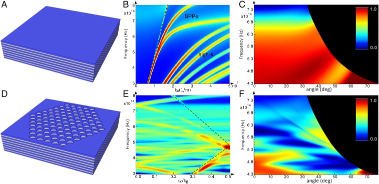
Metamaterials designed to have hyperbolic dispersion have been used extensively to control spontaneous emission (6–10) and are subsequently known as hyperbolic metamaterials (HMMs). These metamaterials are characterized by the hyperbolic shape of their isofrequency surface due to the emergence of high-momentum wave-vector states known as high-k modes (11). An artificial material supporting high-k modes can be realized using alternating metal/dielectric layers with deep-subwavelength thickness (11, 12). A schematic of such an HMM composed of silver (Ag) and alumina (Al2O3) is shown in Fig. 1A along with the mode dispersion in Fig. 1B for a seven-period structure. The system possesses high-k plasmonic bands for , as well as two surface-plasmon-polariton (SPP) modes close to the light line (dashed). The existence of high-k modes provides multiple decay channels for dipole emitters placed inside or on top of the HMM, thereby enhancing the local photonic density of states (LPDOS) and increasing the rate of spontaneous emission (13). Due to the nonresonant nature of the LPDOS enhancement, HMMs are an ideal platform for applications that require broadband control of light–matter interaction.
Fig. 1.
Bandstructure and reflectivity. (A) Schematic of HMM composed of multiple periods of Ag and Al2O3. (B) Bandstructure of HMM. Light line is marked as a dashed line. Two SPP modes are noticeable near the light line. The remaining modes are coupled bulk plasmons known as high-k modes that are characteristic of HMMs. (C) Simulated reflectivity of a plane-wave source from an HMM. The black circle marks the edge of the source angle for a given frequency (SI Appendix, section 2). (D) Schematic of PHC. Two-dimensional periodic arrays of holes in a triangular lattice are defined on the HMM extending down through the first two periods. (E) Bandstructure of PHC. Folding of bands accompanied by intermodal coupling is observed below the light line. (F) Simulated reflectivity of a PHC. The wide blue regions mark angle and frequency ranges for which reflectivity drops near zero, indicating efficient in-/outcoupling of light. The two thin faint bands in the upper portion of the graph are the −1 diffraction order of the two SPPs which appear in B.
Despite the attractiveness of the aforementioned features, the use of HMMs in realizing practical devices has been hindered due to the fact that the high-k modes lie below the light line; hence, the coupled radiation cannot propagate to the far field and is eventually dissipated through ohmic loss. The situation is demonstrated in Fig. 1C by the high reflectivity of the metamaterial, where the simulated reflectivity of a plane wave is plotted as a function of frequency and source angle. It is seen that HMM structures are omnidirectionally highly reflective, indicating that no coupling to high-k modes can be achieved from free space, or reciprocally, high-k modes cannot propagate into free space. Indeed, for embedded dipole emitters, typically less than 1% of the total power can escape to the far field (14). To alleviate this issue, different approaches such as diffraction gratings and nanopatterning have been used to achieve modest enhancement in light extraction/coupling efficiency from light emitters embedded in HMMs (14–17).
In the present work, we use the PHC concept to exploit LPDOS enhancement offered by the hyperbolic dispersion while simultaneously enhancing light outcoupling as well. A schematic of a 2D PHC is shown in Fig. 1D, where a periodic subwavelength lattice of holes is patterned onto an HMM. The periodicity folds the high-k modes inside the light line, as shown through finite difference time domain (FDTD) simulations in Fig. 1E. This enables efficient outcoupling of the high-k states that were previously below the light line. The corresponding reflectivity map (Fig. 1F) of the PHC now shows multiple regions with near-zero reflectivity, indicating broadband and wide-angle light coupling to the structure. It is the complex interaction between multiple folded modes in the PHC that results in the enhanced outcoupling that is observed in this paper. Equally important is the fact that the LPDOS in the HMM is not significantly altered by the structural modification. This is shown in SI Appendix, section 3 through 3D FDTD calculations for the Purcell factor of an emitter embedded in PHC and HMM.
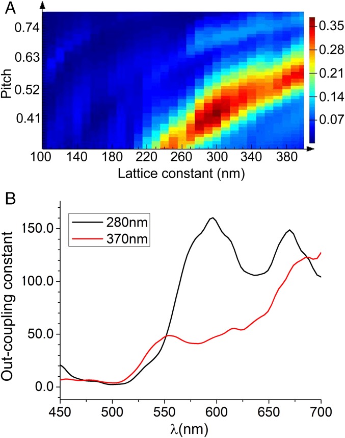
To optimize the design of a PHC for outcoupling of light from the embedded quantum emitters, 2D and 3D FDTD simulations are used (see Methods for details). A parametric sweep is performed over the pitch and lattice constant of the PHC with the goal of maximizing the output power for a dipole embedded inside the HMM. Fig. 2A shows a color map which plots the portion of outcoupled power into a 60° half-angle (corresponds to 0.8-N.A. objective used in the experiments) for a wavelength of 630 nm, which corresponds to the emission peak of the QDs used in the experiment (see SI Appendix, section 1, QD emission spectrum). We see that for this wavelength, maximum outcoupling is achieved for lattice spacing a = 280–300 nm and pitch of 0.42, corresponding to a hole radius of ∼60 nm. In Fig. 2B we show the wavelength-resolved outcoupling contrast ratio for PHCs with a = 280 and 370 nm and a pitch of 0.42. The outcoupling contrast is simply defined as the power transmitted to the far field by an emitter embedded in PHC versus the same emitter embedded in HMM. We observe that for a wide spectral range between 575 and 700 nm the outcoupling contrast exceeds 100.
Fig. 2.
Outcoupling simulations. (A) Simulation of far-field transmitted power fraction from an embedded dipole into a 0.8-N.A. objective. (B) Simulation of outcoupled contrast from embedded dipole measured as PHC transmitted power/HMM transmitted power. Black curve for lattice constant a = 280 nm; red curve for a = 370 nm.
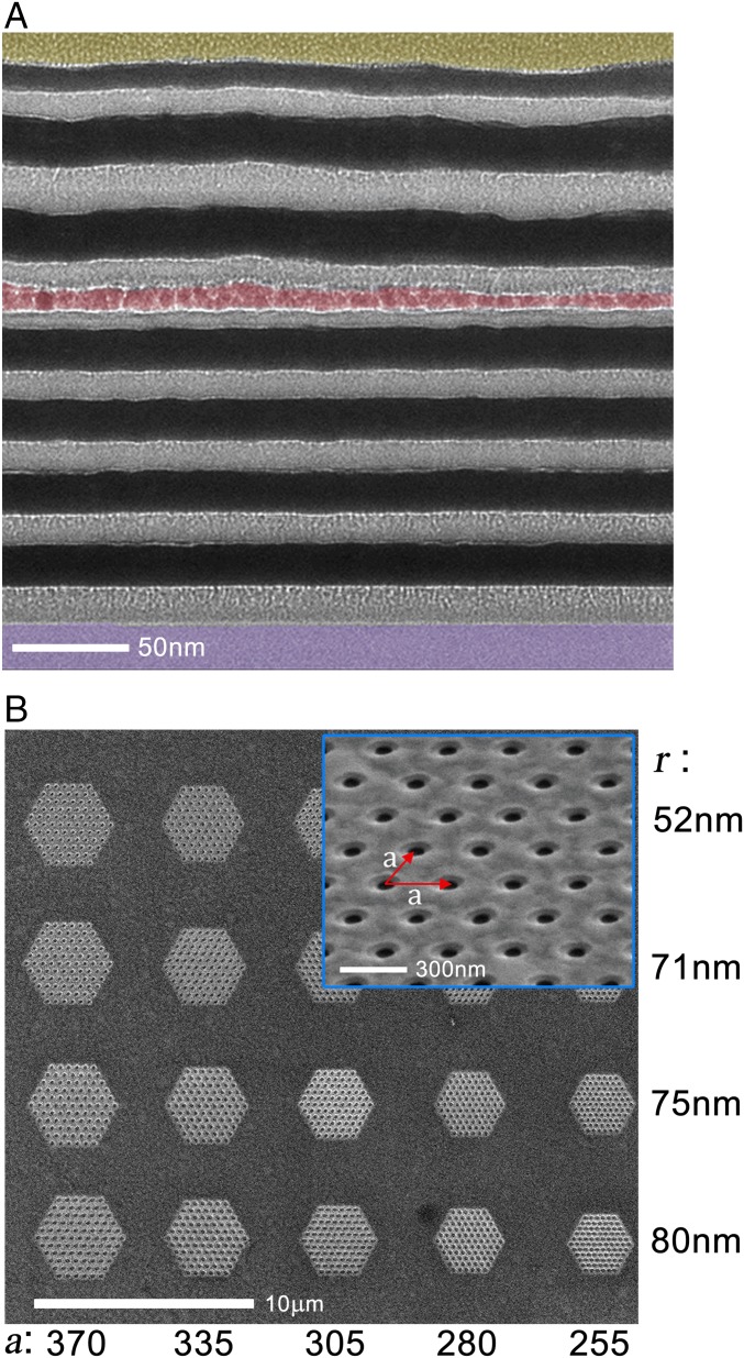
The HMM structure used in the present work consists of seven periods of Ag (ε < 0) and Al2O3 (ε > 0) with average thickness of 15 nm with colloidal CdSe/ZnS QDs embedded inside the fifth dielectric layer. Very thin germanium (∼1 nm) is used as a seed layer before the deposition of Ag for achieving ultrasmooth, consistent thin films (18). In Fig. 3A a cross-sectional transmission electron microscope image of the structure shows the alternating layers along with the embedded QD layer. The effective dielectric constants of this structure are shown in SI Appendix, Fig. S1A. The emission wavelength of the QDs (630-nm center of emission) is specifically chosen to be in the hyperbolic dispersion range (SI Appendix, Fig. S1B). The location of the QD layer has been carefully selected to provide maximum coupling to plasmonic modes while keeping a distance of ∼6 nm from the nearest metallic layer to avoid quenching (13). To realize the PHCs, focused ion-beam milling is used to etch hexagonal arrays of holes into the HMM structure with varying lattice constant a and radii r. A scanning electron microscope image of the array of PHCs is shown in Fig. 3B along with a magnified image of one of the PHCs (Inset). The holes are milled through the top two silver layers and terminated before the QD layer.
Fig. 3.
Cross-section and top view. (A) Transmission electron microscope image of cross-section of HMM. Bottommost and topmost layer are glass substrate and Pt protection layer, respectively (shown in false color); dark layers are Ag and bright layers are Al2O3. The QD layer (shown in false color) is visible in the fifth dielectric layer from the bottom. (B) SEM image of patterned PHCs. The lattice spacing is decreased from left to right and the hole radius is increased from top to bottom. (Inset) Magnified image of one of the PHCs and the direction of the lattice constants.
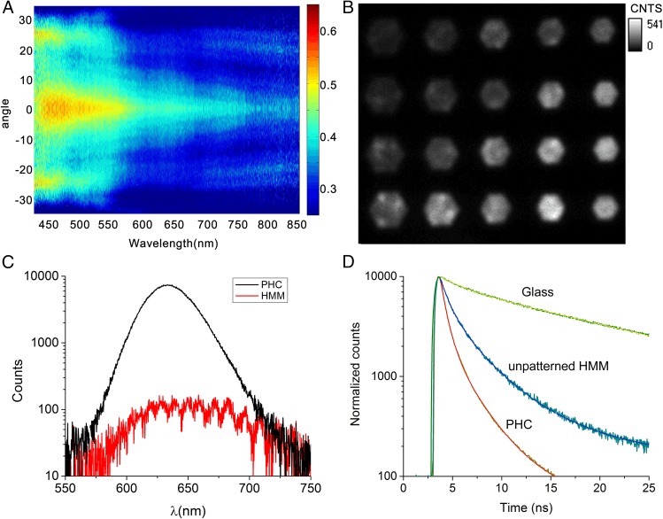
Fig. 4A shows an angle-resolved white-light reflectivity image obtained by Fourier space (k-space) imaging (details in SI Appendix, section 4) of the PHC with a = 280 nm and r = 80 nm. The reflectivity is normalized with respect to the HMM substrate using the following formula:
| [1] |
Rp is termed partial reflectivity, RHMM is reflectivity from HMM, and RPHC is reflectivity from PHC. We can see that the response of the 280-nm-period PHC (Fig. 4A) extends in a narrow range of angles from 580 to 750 nm allowing for increased outcoupling in that range. The range overlaps the emission spectrum of the embedded QDs. The larger-period PHCs do not exhibit this narrow band of transmission (see SI Appendix, section 3 for k-space image of larger period and real-space reflectivity graphs).
Fig. 4.
Intensity and lifetime of emission. (A) k-space white-light reflection image from a = 280 nm, r = 80 nm PHC normalized to reflection from HMM background. (B) PL intensity map of array of PHCs. Strongest outcoupling is observed for the PHC with a = 280 nm and r = 80 nm. Color scale represents fluorescence counts. (C) Steady-state emission spectrum of PHC and HMM. The observed wiggles in the HMM are due to interference effect from the emission filter in the optical path. (D) Lifetime kinetics of QDs embedded in PHC, HMM, and QDs on a glass substrate. The respective lifetimes are 1.28, 2.97, and 25 ns.
Photoluminescence (PL) measurements from the active PHCs were carried out using a home-built confocal microscope for fluorescence-lifetime imaging microscopy (FLIM), a technique which allows simultaneous mapping of intensity and lifetime for every pixel of the fluorescence image, thus providing spatial, temporal, and steady-state emission properties of the active PHC structure. Shown in Fig. 4B is a PL intensity image of the array of PHCs. We see a clear dependence of the emission intensity on lattice constants and radii of the holes with the maximum emission intensity observed for a = 280 nm and radius r = 80 nm. Fig. 4C shows the steady-state emission spectra of the HMM and the PHC. A 100× enhancement factor in emission intensity is observed due to the outcoupling of the high-k states by the PHC structure. Another important attribute is that the outcoupling efficiency is a broadband effect. Unlike a conventional PC defect cavity that relies on narrow-band resonance, the PHC enhances and outcouples the entire spectral range of the QDs.
Shown in Fig. 4D are the time-resolved emission traces for QDs on glass compared with QDs in HMM and PHC. The spontaneous emission lifetimes of QDs in HMM and PHC are strongly modified with respect to QDs on glass by factors of 9 and 20, respectively. The reason for the observed difference between PHC and HMM is that the outcoupled light in PHC is preferentially composed of emission from the vertically oriented dipoles of the QD film which are better coupled to the transverse magnetic polarized high-k modes and therefore experience larger enhancement and better outcoupling to the far field.
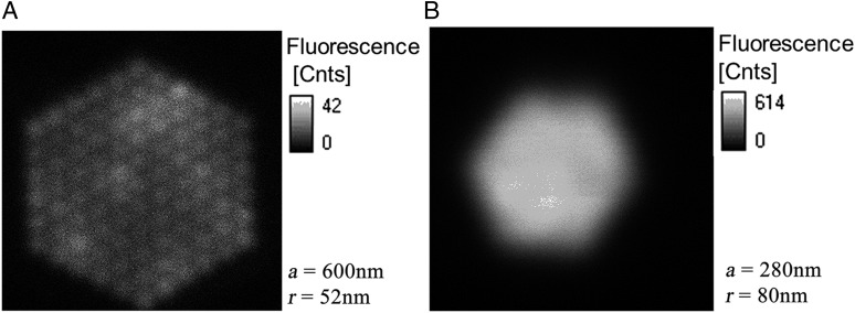
To further substantiate that the collective modes of the hypercrystal are responsible for the enhanced emission from the PHC, we investigated structures where the lattice spacing was large enough (600 nm) for each of the holes to act as an individual scatterer. This structure shows a small enhancement factor of 7× as shown in Fig. 5A, in contrast to the PHC structure with lattice constant of 280 nm where strong coupling between the fields around the nanoholes leads to outcoupling efficiency of 100× (Fig. 5B). The result is consistent with our simulations (Fig. 1E) showing the appearance of coupled modes in the PHC structure which are responsible for the large outcoupling enhancement.
Fig. 5.
PL images. (A) Image of PHC with a = 600 nm and r = 52 nm, where each nanohole can be seen to act as an independent scatterer. (B) Image of PHC with a = 280 nm and r = 80 nm, where strong coupling between nanoholes leads to formation of a supermode and hence improved outcoupling efficiency.
In summary, we have demonstrated a class of artificial photonic medium: the PHC. We show how one can independently engineer the LPDOS using the hyperbolic dispersion of the metamaterial and the light outcoupling using subwavelength-sized lattice geometry. Enhancement in light extraction by a factor of 100 and spontaneous emission rate by a factor of 20 is seen from QDs embedded in the PHC structure. Furthermore, our PHC structures show broadband enhancement in light outcoupling and spontaneous emission rate, thus providing an ideal platform for applications that require nonresonant control over light–matter interaction such as in solar cells, ultrafast light-emitting diodes, and single-photon sources.
Methods
Fabrication.
HMM substrates were grown by a Kurt Lesker PVD 75 electron-beam evaporation system on top of precleaned glass substrates with surface roughness <1 nm. The pressure inside the vacuum chamber was kept to ∼5 × 10⁻⁶ torr throughout the process. As a part of the calibration and characterization process, thin films of Al2O3 and Ag with Ge seed were grown and optically characterized by a J.A. Woollam M-2000 ellipsometer. The measured optical constants (included in SI Appendix) were used in our analytical calculations and FDTD simulations.
PL and Lifetime Measurements.
Intensity and lifetime measurements were taken on a modified Olympus IX-81 microscope using an FLIM technique. The QDs are pumped by a 440-nm pulsed diode laser at 40-MHz repetition rate with 90-ps pulse width. The emission from the QDs is spectrally separated from the laser by a Semrock RazorEdge 532 long-pass filter and detected by an Avalanche photodiode coupled to a PicoHarp 300 time analyzer. This setup allows us to detect the intensity and the lifetime at any spot on the sample. The sample is mounted on a piezo-controlled stage with a maximum scan area of 80 µm × 80µm. SymphoTime 64 software is used to obtain intensity and lifetime maps of the sample.
FDTD Simulations.
Simulations model the quantum emitter as an electric dipole oriented parallel or perpendicular to the metal-dielectric layers of the HMM/PHC with an emission spectrum extending from 0.3 to 1.2 μm. As a first step to PHC design, 2D FDTD simulations are carried out with a double parameter sweep (hole radius and periodicity) to maximize the outcoupled power for the wavelength corresponding to the emission maximum of the QDs. Full 3D simulations are also carried out to obtain meaningful values of the hole radius and periodicity to ensure a realistic design. The simulations also calculate the Purcell factor of the dipole and the spatial distribution of the electric field, both as a function of wavelength (see SI Appendix, section 3).
For details on bandstructure and reflectivity simulations, see SI Appendix, section 2.
Supplementary Material
Acknowledgments
T.G. and V.M.M. thank Achanta Venu Gopal for useful discussions related to the simulations. We acknowledge the support of Army Research Office (ARO) W911NF-15-1-0019 (to T.G. and V.M.M.) and ARO W911NF-14-1-0639 (to E.E.N.); National Science Foundation (NSF) Division of Materials Research (DMR) Materials Research Science and Engineering Centers Program Grant DMR-1120923 (to V.M.M. and E.E.N.); NSF DMR 1629276 (to E.E.N.); and the Gordon and Betty Moore Foundation (E.E.N.). Research was carried out in part at the Center for Functional Nanomaterials, Brookhaven National Laboratory, which is supported by the US Department of Energy, Office of Basic Energy Sciences, under Contract DE-AC02-98CH10886.
Footnotes
The authors declare no conflict of interest.
This article is a PNAS Direct Submission.
This article contains supporting information online at www.pnas.org/lookup/suppl/doi:10.1073/pnas.1702683114/-/DCSupplemental.
References
- 1.Narimanov EE. Photonic hypercrystals. Phys Rev X. 2014;4:041014. [Google Scholar]
- 2.Narimanov EE. Dirac dispersion in photonic hypercrystals. Faraday Discuss. 2015;178:45–59. doi: 10.1039/c4fd00207e. [DOI] [PubMed] [Google Scholar]
- 3.Hafezi M, Mittal S, Fan J, Migdall A, Taylor JM. Imaging topological edge states in silicon photonics. Nat Photonics. 2013;7:1001–1005. [Google Scholar]
- 4.Smolyaninova VN, Yost B, Lahneman D, Narimanov EE, Smolyaninov II. Self-assembled tunable photonic hyper-crystals. Sci Rep. 2014;4:5706. doi: 10.1038/srep05706. [DOI] [PMC free article] [PubMed] [Google Scholar]
- 5.Kruk SS, et al. Magnetic hyperbolic optical metamaterials. Nat Commun. 2016;7:11329. doi: 10.1038/ncomms11329. [DOI] [PMC free article] [PubMed] [Google Scholar]
- 6.Tumkur T, et al. Control of spontaneous emission in a volume of functionalized hyperbolic metamaterial. Appl Phys Lett. 2011;99:151115. [Google Scholar]
- 7.Kim J, et al. Improving the radiative decay rate for dye molecules with hyperbolic metamaterials. Opt Express. 2012;20:8100–8116. doi: 10.1364/OE.20.008100. [DOI] [PubMed] [Google Scholar]
- 8.Krishnamoorthy HNS, Jacob Z, Narimanov E, Kretzschmar I, Menon VM. Topological transitions in metamaterials. Science. 2012;336:205–209. doi: 10.1126/science.1219171. [DOI] [PubMed] [Google Scholar]
- 9.Shalaginov MY, et al. Broadband enhancement of spontaneous emission from nitrogen-vacancy centers in nanodiamonds by hyperbolic metamaterials. Appl Phys Lett. 2013;102:173114. [Google Scholar]
- 10.Molesky S, Dewalt CJ, Jacob Z. High temperature epsilon-near-zero and epsilon-near-pole metamaterial emitters for thermophotovoltaics. Opt Express. 2013;21(January) Suppl 1:A96–A110. doi: 10.1364/OE.21.000A96. [DOI] [PubMed] [Google Scholar]
- 11.Jacob Z, Alekseyev LV, Narimanov E. Optical hyperlens: Far-field imaging beyond the diffraction limit. Opt Express. 2006;14:8247–8256. doi: 10.1364/oe.14.008247. [DOI] [PubMed] [Google Scholar]
- 12.Podolskiy V, Narimanov E. Strongly anisotropic waveguide as a nonmagnetic left-handed system. Phys Rev B. 2005;71:201101. [Google Scholar]
- 13.Newman WD, Cortes CL, Jacob Z. Enhanced and directional single-photon emission in hyperbolic metamaterials. J Opt Soc Am B. 2013;30:766. [Google Scholar]
- 14.Galfsky T, et al. Active hyperbolic metamaterials : Enhanced spontaneous emission and light extraction. Optica. 2015;2:62–65. [Google Scholar]
- 15.Sreekanth KV, Krishna KH, De Luca A, Strangi G. Large spontaneous emission rate enhancement in grating coupled hyperbolic metamaterials. Sci Rep. 2014;4:6340. doi: 10.1038/srep06340. [DOI] [PMC free article] [PubMed] [Google Scholar]
- 16.Lu D, Kan JJ, Fullerton EE, Liu Z. Enhancing spontaneous emission rates of molecules using nanopatterned multilayer hyperbolic metamaterials. Nat Nanotechnol. 2014;9:48–53. doi: 10.1038/nnano.2013.276. [DOI] [PubMed] [Google Scholar]
- 17.West PR, et al. Adiabatically tapered hyperbolic metamaterials for dispersion control of high-k waves. Nano Lett. 2015;15:498–505. doi: 10.1021/nl5038352. [DOI] [PubMed] [Google Scholar]
- 18.Logeeswaran Vj, et al. Ultrasmooth silver thin films deposited with a germanium nucleation layer. Nano Lett. 2009;9:178–182. doi: 10.1021/nl8027476. [DOI] [PubMed] [Google Scholar]
Associated Data
This section collects any data citations, data availability statements, or supplementary materials included in this article.


