Abstract
Biological cells are characterized by highly complex phenomena and processes that are, to a great extent, interdependent. To gain detailed insights, devices designed to study cellular phenomena need to enable tracking and manipulation of multiple cell parameters in parallel; they have to provide high signal quality and high spatiotemporal resolution. To this end, we have developed a CMOS-based microelectrode array system that integrates six measurement and stimulation functions, the largest number to date. Moreover, the system features the largest active electrode array area to date (4.48×2.43 mm2) to accommodate 59,760 electrodes, while its power consumption, noise characteristics, and spatial resolution (13.5 μm electrode pitch) are comparable to the best state-of-the-art devices. The system includes: 2,048 action-potential (AP, bandwidth: 300 Hz to 10 kHz) recording units, 32 local-field-potential (LFP, bandwidth: 1 Hz to 300 Hz) recording units, 32 current recording units, 32 impedance measurement units, and 28 neurotransmitter detection units, in addition to the 16 dual-mode voltage-only or current/voltage-controlled stimulation units. The electrode array architecture is based on a switch matrix, which allows for connecting any measurement/stimulation unit to any electrode in the array and for performing different measurement/stimulation functions in parallel.
Index Terms: high-density microelectrode array (HD-MEA), neural interface, multi-functionality, high channel count, low noise, low power, switch matrix, extracellular recording and stimulation, neurotransmitter detection, impedance spectroscopy, pre-charging, pseudo-resistor
I. Introduction
Electrogenic cells, such as neuronal, cardiac, and pancreatic cells are capable of generating and transmitting electrical signals. The flow of ions through the cell membrane generates changes in electrical potentials that can be measured using standard electronic circuitry. Apart from electrical signals, cells also use chemical compounds for signaling, as it is the case in neuronal synapses (contacts between neuronal cells). The chemicals that transmit signals across the synaptic cleft, so-called neurotransmitters, play a significant role in brain diseases, such as schizophrenia, Alzheimer's, and Parkinson's disease [1]; their presence is detectable by means of electrochemical methods, typically, cyclic voltammetry, [2]–[4]. To study cell network dynamics, a bidirectional interaction, which also includes electrical stimulation of cells, is desired. To ensure precise and selective stimulation of individual neurons, characterization of the electrodes [5], the cell-electrode attachment, and the cell morphology [6] is first performed, typically by means of impedance spectroscopy [7]. This method can also be used for investigation of anisotropic and inhomogeneous electrical conductivity of tissue and culture medium, label-free detection of cancer [8], [9] and studies of neurodegenerative diseases [10]. Simultaneous examination of electrical and chemical cell signaling noninvasively over extended periods of time, performing targeted electrical stimulation, and tracking cellular movements or changes in the electrical interface via changes of impedance, will provide valuable insights in the behavior of individual cells and cell ensembles and help diagnose and treat different disorders.
Microelectrode arrays (MEAs) are well-established platforms for in vitro, extracellular investigation of electrogenic cells that feature multiple electrodes for parallel electrical recording and stimulation [11]–[22]. They are widely used for investigations of cell cultures and cell tissues, such as organotypic brain slices and retinae [14]–[16]. Various MEA systems have been developed to date, featuring different substrates, numbers of electrodes, and electrode pitches [23]. Owing to the small feature size of CMOS technology, recent CMOS-based MEA systems comprise thousands of electrodes at pitches of tens of μm, down to a few μm [18]–[22], which is crucial to obtain detailed insights into cellular and sub-cellular phenomena [24]. The two most common CMOS-MEA architectures base either on the in-pixel front-end amplifiers [19]–[21], or on the switch matrix [18], [22], where the amplifiers reside outside of the electrode array and are connected to the electrodes via a programmable matrix of switches. Both approaches have been detailed and compared in [23].
Contemporary MEAs feature up to three different types of measurement/stimulation functions. The HD-MEAs in [18]–[22] feature only voltage recording and/or voltage/current stimulation; they are limited either in the noise performance [19]–[21], spatial resolution [20], or number of readout channels [18]–[22]. The systems in [2]–[4], [6] feature a combination of neurotransmitter, impedance and/or electrophysiology measurement functions, however, they have a very low number of channels, low spatial resolution and no stimulation capabilities.
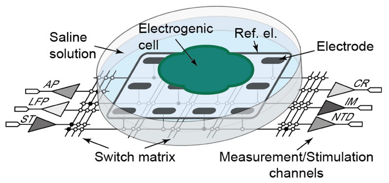
In this paper, we present a high-density MEA system that allows performing multiple measurement/stimulation functions in parallel (Fig. 1). The implemented switch-matrix approach [18], [22] allows connecting any electrode to any of the measurement/stimulation channels. Moreover, the system significantly advances some of the characteristic MEA features. The paper is organized as follows. The system architecture, its functional units, and their integration into a single system are described in Section II, III, and IV, the electrical and biological measurements are described in Sections V and VI, while Section VII gives a detailed comparison to the state-of-the-art and concludes the paper.
Fig. 1.
Illustration of the multi-functional, switch-matrix-based HD-MEA system featuring action potential (AP) readout, local field potential (LFP) readout, current readout (CR), impedance measurement (IM), neurotransmitter detection (NTD) and stimulation (ST) channels.
II. System Architecture
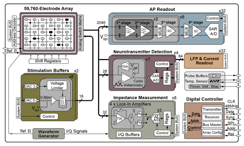
An overview of design requirements for the different functional units is shown in Table I. The number of measurement/stimulation channels is limited by the chip area and overall power consumption. The processes of neuronal cells can extend over a few hundred μm (Purkinje neurons) and more, hence, to explore functional connections in fairly distant regions of tissue slices (mm distance), we have opted for at least 4×2 mm2 of active electrode array area. The data sampling frequency of 20 kS/s has been chosen based on the frequency range of extracellular signals of different cells, including neuronal action potentials (APs), 300 Hz-10 kHz, neuronal local field potentials (LFPs), 1 Hz-300 Hz, and cardiac APs, 1 Hz-1 kHz. To prevent cells heating by more than 2 °C, the targeted power consumption was below 100 mW. The block diagram of the overall system is depicted in Fig. 2. The details on each of the functional units are given in the next section, with the exception of the current recording unit, which will not be covered here due to space limitations.
Table I.
Overview of design requirements for different measurement/stimulation units
| Function | Function Type | Spatial Resolution | Signal Level | Signal Frequency | Noise & Linearity | Number of Channels |
|---|---|---|---|---|---|---|
| AP Readout | Electrical: Action-potential recording | Sub-cellulara, b | Neuronal AP: <1 mV | Neuronal AP: 300 Hz-6 kHz | <5 μVRMSc | Thousands |
| LFP Readout | Electrical: Local-field potential recording | Few hundred μmd | Neuronal LFP: <5 mV. Cardiac/pancreatic AP/LFP: tens of mV | Neuronal LFP: ~1 Hz - 300 Hz, Cardiac AP: ~1Hz-1 kHz. | <10 μVRMS | Few tens |
| Neurotransmitter Detection | Electrochem: Neurotransmitter detection | Sub-cellular/cellulara | nA - μA | ~10 kHz for FSCV | <0.5 nARMS | Few tens |
| Impedance Meas. | Electrical/Electrochem: Cell-electr. interface characterization | Sub-cellulara | 10 kΩ-10 GΩ | 1 Hz-1 MHz | <1.0 pARMS | Few tens |
| Stimulation | Electrical: Evoking activity by applying voltage/current pulse | Sub-cellulara | Voltage:±1.3V Current: ±30μA in low range, ±300 μA in high range | 10 kHz – 100 kHz for single electrode | >9 bit linearity | Few tens |
| Current Readout | Electrical: Current recording | Sub-cellulara | pA | - | <100 fARMS | Few tens |
Cell diameters: few μm to few tens of μm.
To closely approach axons (weak signals, ~20 μV, [26]) and track cellular morphological changes (e.g., axonal initial segment [25]).
Fig. 2.
Block diagram of the multi-functional MEA system.
III. Functional Units
A. Electrode Array
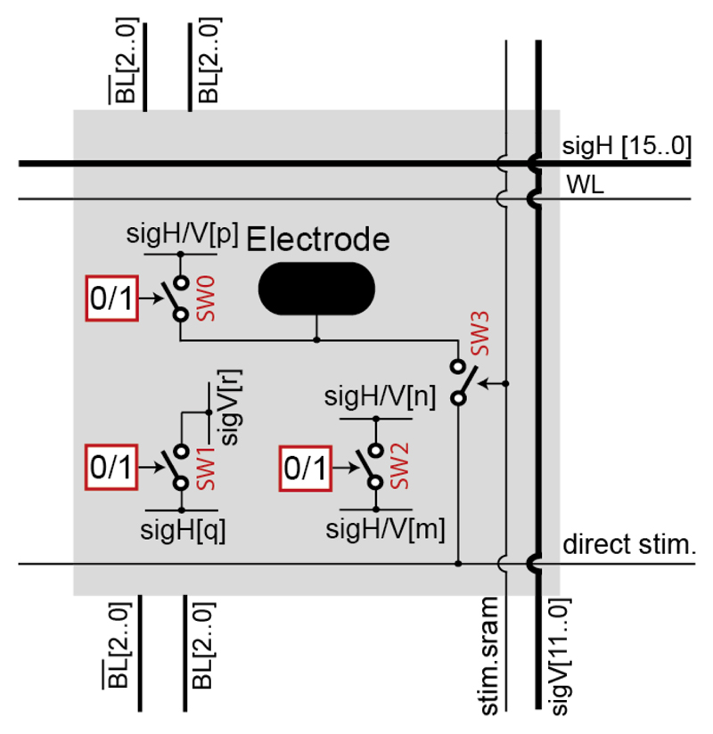
The electrode array features 59,760 microelectrodes (3.0×7.5 μm2), distributed over 332×180 pixels, at a 13.5 μm pitch (5,487 electrodes/mm2), covering an area of 4.48×2.43 mm2. The electrode array was organized in pixels (Fig. 3), and the underlying electrode routing was switch-matrix-based [18], [22]. Each pixel contained 4 transmission gates with approximately 600 Ω on-resistance, and 3 SRAM cells. The SRAM cells were used to set the state of three switches (SW0-SW2) that connected either the electrode to a signal wire or pairs of wires. The fourth switch (SW3) was used to connect the electrode to a stimulation unit using a low-impedance routing path, which contained only two switches. The largest possible high-density (HD) electrode block consisted of 45×45 pixels (607.5×607.5 μm2, 2025 pixels), containing 4 times more pixels and covering twice the area of the largest HD block in [22]. The more advanced features of this switch matrix came from the more advanced CMOS technology used (0.18 μm, instead of 0.35 μm), and from the particular switch arrangement implemented. The arrangement of the switches in the electrode array achieved a maximal routing flexibility, so that any electrode could be connected to any measurement/stimulation channel. Additionally, different electrodes can be simultaneously routed to different measurement/stimulation units, which enables conducting complex experiments, targeting different cell features in parallel. The array switch pattern also allows for locally connecting multiple electrodes (e.g., 4, 9, or 16 electrodes) to obtain a sensing area of rectangular shape and arbitrary size. These pseudo-large electrodes enable charge integration over a large area, which can be used in recording LFPs and may prove beneficial in neurotransmitter detection.
Fig. 3.
Block diagram of an array pixel. Switch SW0 connects the electrode to either a horizontal (sigH) or a vertical (sigV) wire. SW1 connects two intersecting wires, SW2 connects a pair of parallel wires. m, n, p, q ∈ [0,15], r ∈ [0,11].
The physical layout of the array was generated using a custom C++ application that described the switch matrix as a mathematical graph. An electrode routing configuration is generated by means of Integer Linear Programming, where the routing is mapped into a max-flow, min-cost problem, similar to [18], [22]. The reconfiguration of the entire array takes up to 4.5 ms.
B. Voltage Recording Channels
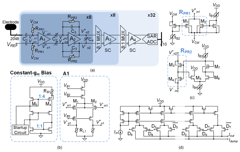
2048 AP recording channels were organized in 32 recording blocks (Fig. 4(a)). Each block consisted of 64 AP channels, including 64 continuous-time (CT) first-stage and second-stage amplifiers, 8 switched-capacitor (SC) third-stage amplifiers, one SC fourth-stage amplifier, and one successive-approximation-register (SAR) ADC. Inside each block, bias circuitry and digital control logic were shared among 16/64 channels. Weak extracellular signals were amplified by the four amplification stages, with a programmable gain from 29 to 77 dB (steps of 6 dB), after which they were sampled at 20 kS/s and digitized by the 10-bit 1.28 MS/s SAR ADC. To suppress interferences from power supplies and substrate, the whole signal chain of the AP recording channel featured fully differential structure.
Fig. 4.
AP recording channels. (a) Block diagram of the 2048 AP recording channels. (b) Open-loop amplifier (A1) used in the first stage and its constant-gm bias circuit. (c) Two types of pseudo resistors and their bias circuits. (d) MOSFET-only R-2R current DAC for tuning high-pass corner frequencies.
As the noise performance of the signal chain was mostly determined by the first stage, about half of the total recording channel power was allocated to this stage to achieve a low noise level. To further reduce the noise, a resistively loaded open-loop topology has been adopted [29][30], [31] (Fig. 4(b)). Traditional CMOS neural amplifiers employ closed-loop topologies with high-gain OTAs, [32], which use PMOS transistors for the input differential pair and NMOS transistors, notorious for flicker noise, for the active loads. Resistors, however, generate no flicker noise and less thermal noise. Therefore, the proposed open-loop topology achieved a lower noise level than traditional topologies with similar power consumption. However, one drawback of this topology is that its gain can vary significantly due to process and temperature (PT) variations. To keep such variations low, a constant-gm biasing circuit was used to generate the tail current of the amplifier A1 (Fig. 4(b)). By matching the PMOS transistors (M1, M2 and M4) and the resistors (RL1, RL2 and RB1) in both A1 and the biasing circuit, a uniform gain was achieved.
The second stage (Fig. 4(a)) employed a closed-loop structure, which provided an accurate gain of AV2 = C2/C3 (programmed by tuning C2) and could handle a large swing. Owing to the relaxed noise requirements, the gm of its input transistors was reduced to cut power consumption, and thus less load capacitance was required to realize the anti-aliasing filtering. The load capacitor, C4, can be tuned to set the low-pass corner frequency to around 6 kHz.
In addition to achieving low noise, the two CT stages had to remove low-frequency (<1 Hz) electrode potential drifts and control their offsets to avoid saturating succeeding amplifiers in large-gain configurations. Therefore, a high-pass filter (HPF, C1 and RPR1) has been implemented in front of the first stage to remove the electrode potential drifts, and the HPF (C3 and RPR2) in the second stage to null the first-stage offset. Due to the DC feedback through RPR2, the offset of the amplifier A2 was divided by AV2 when referred to the input of the second stage, and further divided by the first-stage gain when referred to the electrode.
Both HPFs had to have very low corner frequencies (fHPF < 10 Hz) to avoid filtering out AP signals and adding excessive noise into the AP band. Nonetheless, C1 and C2 had to be around a few pF due to area constraints, and, thus, RPR1 and RPR2 had to be in the TΩ range. Such large resistances are usually realized with so-called “pseudo-resistors”, i.e., MOS transistors biased in the weak inversion region. However, in conventional structures, the transistor gates are biased with fixed voltages, and, hence, threshold voltage (VT) variations, resulting from PT variations, produce large resistance variations. To guarantee a good uniformity of fHPF, two pseudo-resistor structures have been devised, [30], [31] (Fig. 4(c)). RPR1 consisted of a PMOS (M1) and an NMOS (M2) transistor connected like a transmission gate. Their gates were biased by a PMOS and an NMOS current mirror, respectively. Hence, the first-order dependence of their overdrive voltages (VOV) on VT has been cancelled. For RPR2 a similar structure as in [33] was adopted, which consists of two NMOS transistors (M3 and M4) connected in series. Here, an NMOS-only level shifter (M5, M6, and M7) was used to bias the gates of M3 and M4, instead of a PMOS level shifter in [33], to obtain a better process tracking. VOV3 was approximately equal to (VOV6 + VOV7 − VOV5) + (VT6 + VT7 − VT5 − VT3), and had a weak dependence on VT. Thus, resistance variations of both RPR1 and RPR2 were substantially smaller than those of the conventional structures. In addition, both RPR1 and RPR2 were designed symmetrically around their common-mode voltages, which entailed a good linearity. Furthermore, the two resistances were inversely proportional to the bias currents (IB1~IB4), which can be tuned to adjust fHPF for compensating PT variations and to accommodate different experimental scenarios. This adjustability was realized by using two 7-bit current DACs (shared by 16 channels, Fig. 4(d)) for two stages. The DACs relied on the current-division principle of MOS transistors and were realized using a compact MOSFET-only R-2R ladder structure [34].
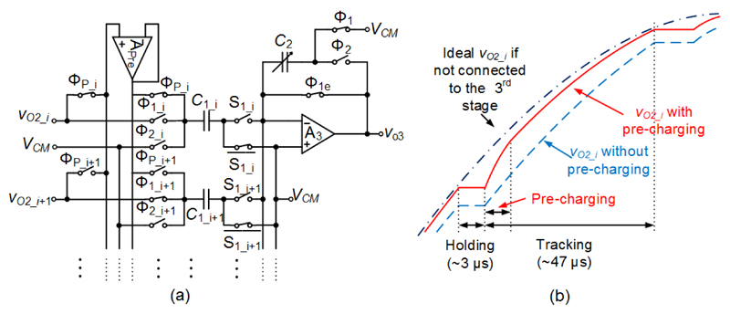
To reduce area and power consumed by the last two stages and the ADCs, 8-to-1 multiplexing has been realized in front of both stages. To ease the implementation of multiplexing and handle large signal swings, the SC topology has been chosen. However, when the CT output of the second-stage amplifier,VO2_i, was connected to an input capacitor of the SC third stage (e.g., C1_i in Fig. 5(a)), VO2_i got disturbed and could not settle to a 10-bit accuracy within the tracking phase (~47 μs), as the second-stage bandwidth was limited to around 6 kHz. To solve this issue a CT buffer could have been added after each second-stage amplifier, but this would have entailed additional power consumption. In this work, a pre-charging amplifier, APre, was connected to VO2_i at the beginning of the tracking phase and drove C1_i (Fig. 5(a)). Thus, VO2_i was disturbed only by a small capacitor (input capacitance of APre << C1_i). At the end of pre-charging, the voltage of C1_i was already quite close to VO2_i (Fig. 5(b)), so that VO2_i could settle to the required accuracy in the remaining tracking phase. As APre was shared among 8 channels, the power overhead was negligible.
Fig. 5.
The pre-charging technique. (a) Schematic of a portion of the SC third-stage amplifier, drawn as single-ended circuit for brevity. (b) A sketch of Vo2_i with/without using the pre-charging technique.
The LFP and AP channels shared a similar topology. The 32 LFP channels have been divided into 4 blocks, each containing 8 CT first- and second-stage amplifiers, one SC third-stage amplifier, and one SAR ADC. The two CT stages featured the same topologies as the AP channels, with high-pass corner frequencies lower than 1 Hz. The third stage and the ADC were the same as those in the AP channels with a reduced clock rate.
C. Neurotransmitter Detection Channels
The neurotransmitter detection (NTD) circuit is based on the fast-scan cyclic voltammetry (FSCV) technique, [35]–[39]. This technique relies on applying a triangular-shape voltage signal with gradients of more than 100 V/s between a working and a reference electrode, and measuring the resulting current flowing through the working electrode. The trace of the measured current versus the applied voltage, i.e., cyclic voltammogram (CV), provides information about the electrochemical properties of the analytes in the cell medium. In this realization, the reference electrode potential was kept constant while the working electrode potential was swept to minimize disturbances to the other measurement units on the chip.
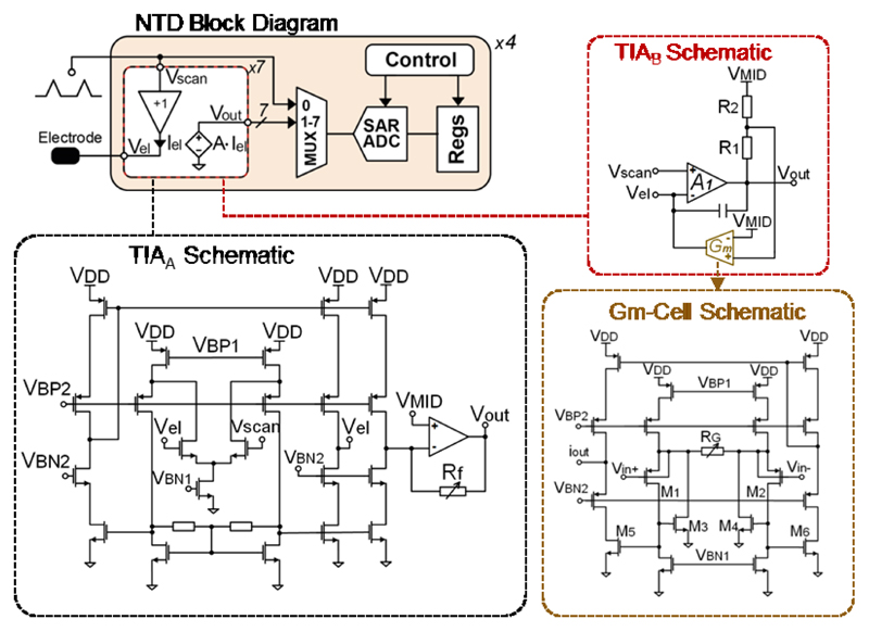
The NTD channels were grouped into 4 blocks, each block consisting of 7 trans-impedance amplifiers (TIAs), which were designed to copy the CV scan voltage to the electrode and measure the electrode current. To maintain the timing information, the scan voltage and the 7 current signals were multiplexed and then sampled at 20 kS/s by a 10-bit SAR ADC.
Two novel TIA circuit topologies were developed: TIAA was designed to record from large electrodes, and TIAB, which featured low noise levels, was tailored to record from small electrodes. Both topologies could scan the working electrode potential within a 2 V window and record currents on the order of μA, at a 10-bit resolution (Fig. 6). TIAA included a local common-mode feedback (LCMFB) OTA, configured in a unity-gain feedback to buffer the input scan voltage, and a resistive TIA. The cascode transistors in the current mirror ensured that the mirrored current closely followed the electrode current (Iel), irrespective of the voltage difference between the electrode and VMID. The TIAA output voltage (Vout) was equal to RfIel, where Rf could be configured as 1 MΩ or 3 MΩ. The OTA inside the TIAA had its dominant pole at the output stage and remained stable even for very large capacitances of the aforementioned pseudo-large electrodes, and rendered slow-rate CV applications possible.
Fig. 6.
Block diagram of the neurotransmitter detection channel and schematics of TIAA, TIAB, and the Gm cell.
TIAB was composed of a two-stage Miller-compensated opamp (A1) and a Gm cell. This topology resembled a resistive TIA, but the feedback resistor was replaced with a linear Gm cell. The Gm cell eliminated the feedforward path passing through the feedback resistor and thus prevented the scan voltage appearing at the output. The linearity of the Gm cells (Fig. 6) was significantly improved by avoiding the body effect of M1 and M2, and keeping VGS1 and VGS2 constant by a local feedback around M1, M3 and M2, M4, [40]. Therefore, the input differential voltage was almost entirely applied across R1 and converted to a current. This current flowed through M3 and M4 and then got mirrored to the output branch. The cascode transistors at the output branch reduced the output current variation due to the scan voltage. The output current of the Gm cell can be calculated as:
where (W/L)5 was equal to (W/L)3 for this design. Since the input impedance of A1 was very high, iout had to exactly match the electrode current. Consequently, the transimpedance of TIAB, RTIA, can be calculated as which can be tuned according to the experimental conditions.
D. Impedance Measurement Channels
The main challenge in integrating many impedance measurement (IM) channels with limited silicon area is to achieve simultaneously low noise level, high dynamic range, and low power consumption. The state-of-the-art IM systems typically trade off large area per channel and power for low noise [41]. Most systems feature exclusively IM channels [42], and only few systems combine both electrophysiology and IM [43], [6]. While [43] reports electrode IM only, [6] reports IM of cardiac cells, however, with a poor spatial resolution.
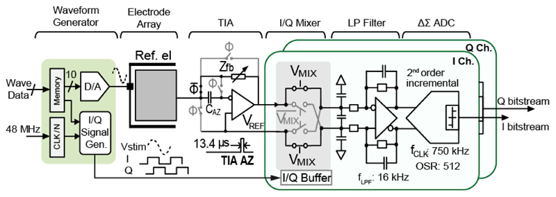
To run IM in real time, a waveform generator with a programmable frequency (1 Hz-1 MHz) and amplitude (set by a 10-bit DAC) was integrated on chip (Fig. 7). The generated sinusoidal voltage (Vstim) was applied between the reference electrode and the selected working electrodes. The resulting current signal from each working electrode (Iel = Vstim/Zel) was converted into a voltage, and the impedance magnitude and phase were reconstructed with a lock-in amplifier, realized by a low-noise TIA and two quadrature phase mixers, followed by a low-pass filter (LPF). The implemented TIA can be programmed with either resistive feedback for measuring large electrodes (impedance < 100 MΩ) or capacitive feedback for measuring electrodes smaller than 10 μm diameter (impedance > 100 MΩ). For the capacitive feedback TIA, a periodic reset [44] was used to avoid the amplifier going to saturation and keep the electrode potential at the reference voltage, VREF. To mitigate the drift of the electrode-electrolyte interface capacitor Ce, and the amplifier offset, the TIA circuitry included an auto zeroing (AZ) function. The amplifier offset was first stored in CAZ (200 fF) during the reset phase, so that during the measurement phase the voltage stored in CAZ canceled the offset and low-frequency drift from the electrode (Fig. 7). The TIA's output signal was mixed with the in- and quadrature-phase (I/Q) signals, which were generated by the waveform generator and phase-locked with Vstim to produce I/Q demodulated impedance signals. A double-balanced passive mixer architecture was selected, since passive mixers normally show higher linearity and negligible 1/f noise compared to their active counterparts [45]. An active differential LPF was used to filter out higher order harmonics and intermodulation products before the A/D conversion. The LPF can be bypassed or its gain set to 1 or 5 by tuning the feedback resistor. The cut-off frequency of the LPF was set to16 kHz, which was about 1/46 of the sampling frequency of the ΔΣ ADC. The I/Q output of the lock-in amplifier was digitized by the incremental single-bit SC ΔΣ ADC, consisting of an on-chip ΔΣ modulator and an off-chip decimation filter. To handle large input signal swing, while relaxing the slewing requirements of the integrators, an input feed-forward (CIFF) topology was employed [46]. Setting the sampling frequency to 750 kHz relaxed the anti-aliasing requirement, and the oversampling ratio was high enough to guarantee a resolution of 14 bits and a temporal resolution of 10 ms upon using proper filtering [41]. To reduce kT/C noise, a large sampling capacitor (1.6 pF) was used. The flicker noise and the offset contributed by the first-stage integrator opamp were suppressed by the AZ technique [47].
Fig. 7.
Schematic of the lock-in-amplifier-based impedance measurement channel.
E. Stimulation Channels
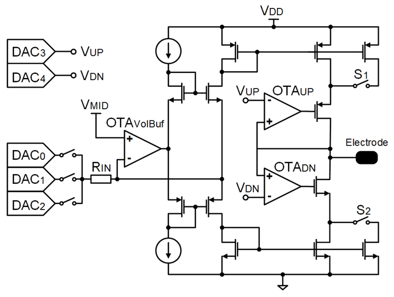
16 stimulation buffers were integrated on the chip, grouped into two blocks of 8. Additionally, each block contained 3 DACs for producing the stimulation waveforms and 2 DACs for setting the limiting voltages, all 5 DACs shared by the 8 stimulation buffers. Each buffer can be configured as voltage-only or current/voltage-controlled buffer. Most reported stimulation buffers provide either voltage- or current-controlled stimulation pulses [48]. Here, the current/voltage-controlled buffers can simultaneously control both the output current and the output voltage. Current-controlled stimulation is desirable for precise charge delivery, independent of the electrode impedance, whereas controlling the stimulation voltage is needed to avoid tissue damage upon exceeding safe stimulation range. Fig. 8 shows the schematic of the stimulation buffer configured in the current/voltage-controlled mode. The core of this circuit is a positive current conveyor of type II (CCII+), an improved version of [49], which converts DAC voltages into electrode currents. The default current range can be increased by closing S1 and S2, which increases the gain of the current mirror in the output stage from 1.0 A/A to about 11.0 A/A. RIN had a value of 50 kΩ, therefore ±1.5 V DAC signal produced ±30 μA in the low-current mode and ±330 μA in the high-current mode. The voltage controllability was realized by OTAUP and OTADN, which turned off either the positive or the negative output current, when the output voltage reached the predefined values of VUP or VDN, respectively. For the voltage-only controlled stimulation, OTAVolBuf was configured in the unity-gain feedback and directly connected to the output. OTAVolBuf used the LCMFB technique as well, and had the dominant pole located at the output node, suited to drive the mainly capacitive electrodes.
Fig. 8.
Schematic of the current/voltage-controlled stimulation buffer.
IV. System Integration
A. Digital Control
A 48 MHz-SPI interface was used to stream the configuration data to the chip, followed by an on-chip cyclic redundancy check (CRC). The measurement/stimulation units and the electrode array were grouped into 26 independently addressable blocks that were interfaced by the on-chip controller using an addressing scheme. As the chip extended over 12.0×8.9 mm2, to guaranty the settling times of the 10-bit-word data generated by the different measurement blocks, the system Read Data Bus was divided into two busses, both running at 24 MHz. The data from the busses were fetched by the controller in an alternating manner at 48 MHz and sent off chip. The order in which the data generated by the measurement units were allocated on the two data busses was defined by the Bus Master module of the digital controller. To avoid data collision, an OR-tree was inserted between the busses and the measurement units. The chip output data was organized in packages, aligned with the sampling cycles, each featuring 2400 10-bit words, ending with a 20-bit CRC checksum.
B. Chip Layout and Fabrication
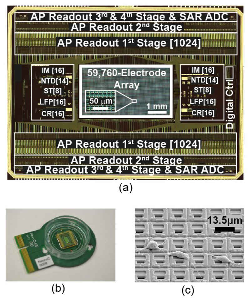
The chip was fabricated in a 0.18 μm CMOS technology (2P6M) and has a size of 12.0×8.9 mm2. The platinum electrodes were post-processed at wafer level by means of ion beam deposition and etching. In the same step, two Pt-resistors used as on-chip temperature sensors were fabricated and implemented in 4-terminal sensing configurations. A multilayer SiO2/Si3N4 passivation stack was deposited by plasma-enhanced chemical vapor deposition (PECVD), on the one hand, to protect the CMOS circuits against the saline solution that was used as cell culture medium, and, on the other hand, to prevent the release of toxic aluminum and copper from the CMOS metal layers into the cell culture. Openings in the passivation, defining the electrode areas and wire bonding contacts, were fabricated in a reactive-ion etching (RIE) step. A shifted-electrode layout [50] was employed to ensure a tight seal between the electrodes in the liquid phase and the CMOS metal layers and circuitry in the chip. Fig. 9 shows the micrograph of the chip, bio-compatible chip packaging, and an SEM image of the post-processed array surface with rat cortical neurons.
Fig. 9.
(a) Chip micrograph. (b) Bio-compatible chip packaging and PCB. (c) SEM image of the chip surface, showing in-house post-processed Pt-electrodes and dissociated primary rat cortical neurons, cultured on top.
V. Electrical Characterization
A. Voltage Recording Channels
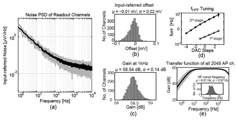
The integrated input-referred noise of an AP recoding channel in the AP band (300 Hz–10 kHz), including the ADC, was 2.4 μVRMS (Fig. 10(a)). The measured maximum input-referred offset ranged from -110 μV to 70 μV, which was achieved without dedicated offset compensation/calibration circuitry [30], [31] (Fig. 10(b)). The measured maximum gain of the recording channel was 76.4 dB. An excellent gain uniformity of σ = 0.14 dB (Fig. 10(c)) was measured by applying a common sinusoidal signal to all inputs. The two tuning curves of the first and second stage HPF corner frequency (fHPF) are illustrated in Fig. 10(d). Fig. 10(e) shows the overall transfer function of all 2048 AP recording channels. The histogram inset demonstrates a good uniformity of fHPF, which indicates a good matching of the pseudo resistors across all channels. Moreover, the SAR ADC achieved an SNDR of 56.2 dB at a sampling rate of 1.28 MS/s and with an input signal frequency of 1.1 kHz. Finally, the measured power consumption of each AP channel was around 16 μW.
Fig. 10.
(a) Noise power spectral density of the AP recording channel including the ADC. (b) Input-referred offset distribution of the 2048 AP channels. (c) Gain distribution of the 2048 AP channels. (d) The first- and second-stage HPF corner frequency (fHPF) tuned by the current DAC. (e) Transfer function of 2048 AP channels and fHPF distribution.
B. Neurotransmitter Detection Channels
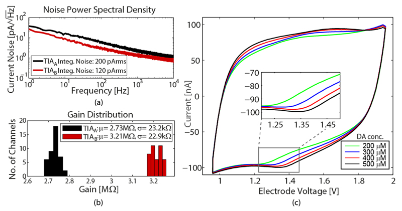
The integrated input-referred noise of TIAA and TIAB, including the multiplexer and the ADC, was 200 pArms and 120 pArms, respectively (Fig. 11(a)). The gain distribution is depicted in Fig. 11(b). In Fig. 11(c), FSCV at 300 V/s using the TIAB was conducted to measure 4 different concentrations of dopamine (DA) in phosphate-buffered saline (PBS, a saline which has similar electrical properties as physiological solution).
Fig. 11.
(a) Noise power spectral density of TIAA and TIAB including multiplexer and ADC. b) Gain distribution across 3 chips. (c) Recorded FSCV results for concentrations of 200 μM, 300 μM, 400 μM and 500 μM dopamine in 0.1 M PBS. TIAB connected to a single electrode has been used. Each of the curves is an average over 98 scans applied within 1 s.
C. Impedance Measurement Channels
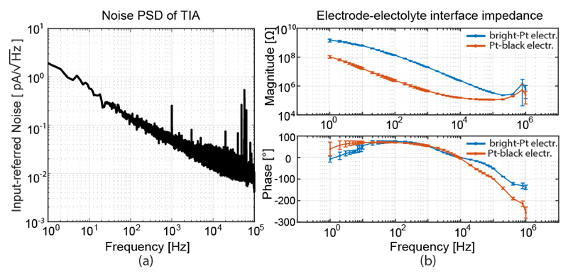
The integrated input-referred noise (1 Hz-100 kHz) of the TIA with a 10 MΩ feedback resistor was 6.4 pARMS (Fig. 12(a)). Pt-electrode-electrolyte interface was characterized in PBS, in a frequency range between 1 Hz and 1 MHz (Fig. 12(b)). The same measurement was repeated after Pt-black electroplating, which was done by driving the current from an external Pt electrode (immersed into the Pt working solution) to the array electrodes, which were shorted to the chip's probe pad (current sink). As expected, in the frequency range from 10 Hz to 10 kHz the impedance showed a 1/f roll-off behavior, which evidenced the dominance of the double-layer capacitance. The predominantly capacitive behavior was also indicated by the phase angle, which ranged between 60-80 degrees. At frequencies over 10 kHz, spreading resistance started dominating the impedance, as the phase angle moved towards zero [50]. The effect of Pt-black deposition was 30-40 fold reduction of impedance magnitude.
Fig. 12.
(a) Noise power spectral density of the TIA with Rf = 10 MΩ. (b) Magnitude and phase of the bright Pt and Pt-black electrode impedance in a frequency range between 1 Hz and 1 MHz, averaged over 6 and 8 electrodes for bright Pt and Pt-black, respectively.
D. Stimulation Channels
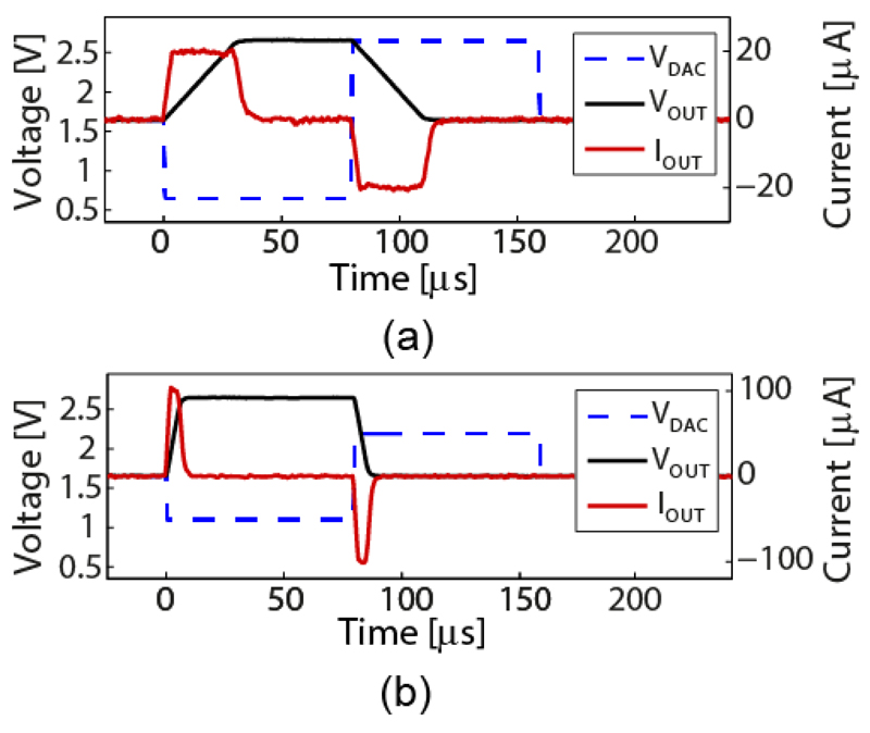
Fig. 13 shows generated current/voltage-controlled pulses using the on-chip stimulation buffers with a load of 610 pF. The output current was switched off when the output voltage reached the predefined limits, in this case 2.65 V for VUP and 1.65 V for VDN. A ±1 V DAC signal resulted in ±20 μA output current for the low-current mode and a ±0.55 V DAC signal resulted in ±100 μA output current for the high-current mode (Fig. 13(a) and (b)). The linearity of the circuit was measured by running a DC sweep, which evidenced a 10-bit linearity for the low-current mode in the range of ±30 μA and a 9-bit linearity for the high-current mode in the range of ±300 μA. The linearity of the voltage-only controlled stimulation, was measured to be 10-bit in the range of ±1.45 V.
Fig. 13.
Voltage (black) and current (red) waveforms, generated by the stimulation buffer operated in current/voltage-controlled mode and connected to a 610 pF external load. The blue dashed line indicates the input waveform. (a) Low-current mode configuration, (b) High-current mode configuration.
VI. Biological Measurement Results
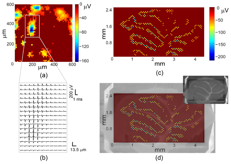
The presented HD-MEA system was verified in in-vitro measurements. Fig. 14(a) depicts average spike amplitudes of dissociated rat cortical neurons (Wistar) recorded by an HD 45×45 pixel electrode block connected to 2025 AP channels. A close-up of the spatial distribution of average AP waveforms, which most likely belong to a single neuron, is plotted in Fig. 14(b). Fig. 14(c) depicts the average activity in a mouse cerebellar slice (C57Bl6J), recorded over the entire array by using a sparse electrode configuration (2000 AP channels, in a honey-comb configuration with an average of ~5.5 pixel spacing between the recording electrodes). Fig. 14(d) shows a superposition of the recorded electrical activity map with a microscopy image of the cerebellar slice. The large number of AP channels featured on the chip enabled a quick overview of the tissue activity by using a single, sparse electrode configuration, which revealed the locations of the electrically active Purkinje neurons [51].
Fig. 14.
(a) Average negative peak amplitudes, recorded by an HD electrode configuration (45×45 pixels, 607.5×607.5 μm2) from dissociated primary rat cortical neurons. Each pixel in the image corresponds to an electrode. (b) AP waveforms, recorded in a sub-region of (a), averaged 20 times. (c) Mouse cerebellar slice electrical activity, recorded with a single sparse configuration of 2000 electrodes. The recording electrodes are displayed 9 times larger than their original size for visual clarity. (d) Overlap of (c) and a microscopy image of the slice (inset).
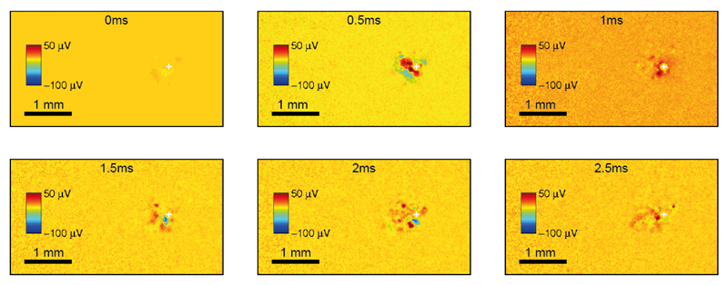
Stimulus–evoked average activity of dissociated rat cortical neurons, triggered by a biphasic voltage pulse of 300 mV amplitude, was recorded over the entire electrode array area at full spatial resolution and depicted in Fig. 15.
Fig. 15.
Six frames showing 2.5 ms of evoked neuronal activity from a culture of dissociated rat cortical neurons. A biphasic voltage-controlled pulse (300 mV phase amplitude and 200 μs phase duration) was applied to a single electrode (white cross), while the other electrodes were scanned for recording from the entire array (4.48×2.43 mm2) at full spatial resolution (13.5 μm electrode pitch). 100 averages were computed for each electrode and temporally aligned with respect to the stimulation pulses.
VII. Conclusion
The presented HD-MEA system includes the largest number of measurement/stimulation functions to date, comprising electrophysiology readout, impedance measurement, and neurotransmitter detection, as well as stimulation capabilities (Table II). At the same time, it features the largest active electrode array area (10.9 mm2) to date, whereas the number of voltage recording channels (2048 AP + 32 LFP), the spatial resolution (13.5 μm electrode pitch), the noise characteristics, and the power consumption are comparable to those of the best state-of-the-art MEA systems. Any measurement/stimulation unit can be connected to any electrode on the array owing to the flexible electrode routing via the switch matrix. The possibility to perform different measurement/stimulation functions in parallel will pave the way to complex experiments that target multiple cellular parameters at once.
Table II.
Comparison to the state-of-the-art MEA systems
| Reference | [19] | [6] | [21] | [22] | This work |
|---|---|---|---|---|---|
| Type | In-pixel Amp | In-pixel Amp | In-pixel Amp | Switch Matrix | Switch Matrix |
| Technology | 0.5 μm | 0.13 μm | 0.18 μm | 0.35 μm | 0.18 μm |
| Active Area | 2.28×1.14 mm2 | 9 pixel groups of 0.128 mm2 | 1×1 mm2/2x2 mm2 | 3.85×2.10 mm2 | 4.48×2.43 mm2 |
| No. Transducers | 32768 | 144 | 4225 / 1024 | 26400 | 59760 |
| No. Different Measurement Modes | 1 | 4 | 1 | 1 | 5 |
| Pixel Pitch | 8.775 μm | 89.4 / 357.8 μmd | 16 / 32 μm | 17.5 μm | 13.5 μm |
| Transducers/mm2 | 12987 | 125 / 7.8 | 977, 3906 | 3265 | 5487 |
| No. Voltage Readout Channels | 32768 | 144 | 4225 | 1024 | 2048 AP + 32 LFP |
| A/D Conversion | 128 pipeline | Off chip | Off chip | 1024 single-slope | 32 + 4 SAR |
| ADC Resolution | 9 bit | - | - | 10 bit | 10 bit |
| Sampling Rate | 2.4 kS/sa | - | 77 (25) kS/sa | 20 kS/s | 20 kS/s |
| Input-referred Noise | - | 12.7 μVrmse | 44 μVrmsb | 2.4 μVrmsb,c | 2.4 μVrmsb,c |
| Total Power | 4 W | - | - | 75 mW | 86 mW |
| Die Size | 9.5×9.5 mm2 | 2.2×2 mm2 | - | 10.1×7.6 mm2 | 12×8.9 mm2 |
When reading out all channels.
Noise integration over 300Hz-10kHz.
Including ADC.
Equivalent square-shaped pixel dimension, for the same spatial density.
Noise integration over 0.5Hz-10kHz.
Acknowledgments
The authors thank M. Ballini, P. Livi, U. Frey, W. Gong, and D. Bakkum, all at ETH Zurich, for discussions and help with neuronal cultures. The authors also thank Evi Bieler, University of Basel, for providing the SEM image.
This work was supported by the ERC Advanced Grant 267351 “NeuroCMOS”. A. Shadmani received individual support through FP7-MTN “EngCaBra” (Contract 264417).
Contributor Information
Jelena Dragas, ETH Zurich, Department of Biosystems Science and Engineering (D-BSSE), 4058 Basel, Switzerland.
Vijay Viswam, ETH Zurich, Department of Biosystems Science and Engineering (D-BSSE), 4058 Basel, Switzerland.
Amir Shadmani, ETH Zurich, Department of Biosystems Science and Engineering (D-BSSE), 4058 Basel, Switzerland.
Yihui Chen, ETH Zurich, D-BSSE, 4058 Basel, Switzerland, and now is with Analog Devices Shanghai Co. Ltd., Shanghai, China..
Raziyeh Bounik, ETH Zurich, Department of Biosystems Science and Engineering (D-BSSE), 4058 Basel, Switzerland.
Alexander Stettler, ETH Zurich, Department of Biosystems Science and Engineering (D-BSSE), 4058 Basel, Switzerland.
Milos Radivojevic, ETH Zurich, Department of Biosystems Science and Engineering (D-BSSE), 4058 Basel, Switzerland.
Sydney Geissler, ETH Zurich, Department of Biosystems Science and Engineering (D-BSSE), 4058 Basel, Switzerland.
Marie Obien, ETH Zurich, Department of Biosystems Science and Engineering (D-BSSE), 4058 Basel, Switzerland.
Jan Müller, ETH Zurich, Department of Biosystems Science and Engineering (D-BSSE), 4058 Basel, Switzerland.
Andreas Hierlemann, ETH Zurich, Department of Biosystems Science and Engineering (D-BSSE), 4058 Basel, Switzerland.
References
- [1].Uhlhaas PJ, Singer W. Review Neural Synchrony in Brain Disorders: Relevance for Cognitive Dysfunctions and Pathophysiology. Neuron J. 2006;52:155–168. doi: 10.1016/j.neuron.2006.09.020. [DOI] [PubMed] [Google Scholar]
- [2].Roham M, Covey DP, Daberkow DP, et al. A wireless IC for time-share chemical and electrical neural recording. IEEE J Solid-State Circuits. 2009;44(12):3645–3658. [Google Scholar]
- [3].Nazari MH, Mazhab-Jafari H, Leng L, Guenther A, Genov R. CMOS neurotransmitter microarray: 96-channel integrated potentiostat with on-die microsensors. IEEE Trans Biomed Circuits Syst. 2013;7(3):338–348. doi: 10.1109/TBCAS.2012.2203597. [DOI] [PubMed] [Google Scholar]
- [4].Guo J, Ng W, Yuan J, Li S, Chan M. A 200-Channel Area-Power-Efficient Chemical and Electrical Dual-Mode Acquisition IC for the Study of Neurodegenerative Diseases. IEEE Trans Biomed Circuits Syst. 2016;10(3):567–578. doi: 10.1109/TBCAS.2015.2468052. [DOI] [PubMed] [Google Scholar]
- [5].Ross JD, O'Connor SM, Blum Ra, Brown Ea, DeWeerth SP. Multielectrode impedance tuning: reducing noise and improving stimulation efficacy. Conf Proc IEEE Eng Med Biol Soc. 2004;6:4115–4117. doi: 10.1109/IEMBS.2004.1404148. [DOI] [PubMed] [Google Scholar]
- [6].Chi T, Park JS, Butts JC, Hookway TA, Su A, Zhu C, Styczynski MP, McDevitt TC, Wang H. A Multi-Modality CMOS Sensor Array for Cell-Based Assay and Drug Screening. IEEE Trans Biomed Circuits Syst. 2015;9(6):801–814. doi: 10.1109/TBCAS.2015.2504984. [DOI] [PubMed] [Google Scholar]
- [7].Buitenweg JR, Rutten WLC, Willems WPA, Van Nieuwkasteele JW. Measurement of sealing resistance of cell-electrode interfaces in neuronal cultures using impedance spectroscopy. Med Biol Eng Comput. 1998;36(5):630–637. doi: 10.1007/BF02524436. [DOI] [PubMed] [Google Scholar]
- [8].Chen Y, Wong CC, Pui TS, et al. CMOS high density electrical impedance biosensor array for tumor cell detection. Sensors and Actuators B Chem. 2012;173:903–907. [Google Scholar]
- [9].Elshafey R, Tlili C, Abulrob A, Tavares AC, Zourob M. Label-free impedimetric immunosensor for ultrasensitive detection of cancer marker Murine double minute 2 in brain tissue. Biosens Bioelectron. 2013 Jan;39(1):220–5. doi: 10.1016/j.bios.2012.07.049. [DOI] [PubMed] [Google Scholar]
- [10].Manickam A, Chevalier A, McDermott M, Ellington AD, Hassibi A. A CMOS electrochemical impedance spectroscopy (EIS) biosensor array. IEEE Trans Biomed Circuits Syst. 2010;4(6 PART 1):379–390. doi: 10.1109/TBCAS.2010.2081669. [DOI] [PubMed] [Google Scholar]
- [11].Thomas CA, Springer PA, Loeb GE, Berwald-Netter Y, Okun LM. A miniature microelectrode array to monitor the bioelectric activity of cultured cells. Exp Cell Res. 1972;74(1):61–66. doi: 10.1016/0014-4827(72)90481-8. [DOI] [PubMed] [Google Scholar]
- [12].Fromherz P. Electrical interfacing of nerve cells and semiconductor chips. ChemPhysChem. 2002;3(3):276–284. doi: 10.1002/1439-7641(20020315)3:3<276::AID-CPHC276>3.0.CO;2-A. [DOI] [PubMed] [Google Scholar]
- [13].Morefield SI, Keefer EW, Chapman KD, Gross GW. Drug evaluations using neuronal networks cultured on microelectrode arrays. Biosens Bioelectron. 2000;15(7–8):383–396. doi: 10.1016/s0956-5663(00)00095-6. [DOI] [PubMed] [Google Scholar]
- [14].Gross GW, Rhoades BK, Azzazy HME, Wu Ming-Chi. The use of neuronal networks on multielectrode arrays as biosensors. Biosens Bioelectron. 1995;10(6):553–567. doi: 10.1016/0956-5663(95)96931-n. [DOI] [PubMed] [Google Scholar]
- [15].Uhlhaas PJ, Singer w. Review Neural Synchrony in Brain Disorders: Relevance for Cognitive Dysfunctions and Pathophysiology. Neuron. 2006;52:155–168. doi: 10.1016/j.neuron.2006.09.020. [DOI] [PubMed] [Google Scholar]
- [16].Stett A, Egert U, Guenther E, Hofmann F, Meyer T, Nisch W, Haemmerle H. Biological application of microelectrode arrays in drug discovery and basic research. Anal Bioanal Chem. 2003 Oct;377(3):486–95. doi: 10.1007/s00216-003-2149-x. [DOI] [PubMed] [Google Scholar]
- [17].Litke M, Bezayiff N, Chichilnisky EJ, et al. What does the eye tell the brain?: Development of a system for the large-scale recording of retinal output activity. IEEE Trans Nucl Sci. 2004 Aug;51(4):14341440. [Google Scholar]
- [18].Frey U, Sedivy J, Heer F, et al. Switch-matrix-based high-density microelectrode array in CMOS technology. IEEE J Solid-State Circuits. 2010;45(2):467–482. [Google Scholar]
- [19].Eversmann B, Lambacher A, Gerling T, Kunze A, Fromherz P, Thewes R. A neural tissue interfacing chip for in-vitro applications with 32k recording / stimulation channels on an active area of 2.6 mm 2. Eur Solid-State Circuits Conf. 2011:211–214. [Google Scholar]
- [20].Berdondini L, Imfeld K, Maccione A, Tedesco M, Neukom S, Koudelka-Hep M, Martinoia S. Active pixel sensor array for high spatio-temporal resolution electrophysiological recordings from single cell to large scale neuronal networks. Lab Chip. 2009;9(18):2644–51. doi: 10.1039/b907394a. [DOI] [PubMed] [Google Scholar]
- [21].Bertotti G, Velychko D, Dodel N, et al. A CMOS-based sensor array for in-vitro neural tissue interfacing with 4225 recording sites and 1024 stimulation sites. IEEE Biomedical Circuits and Systems Conference (BioCAS) Proceedings. 2014:304–307. [Google Scholar]
- [22].Ballini M, Muller J, Livi P, et al. A 1024-channel CMOS microelectrode array with 26,400 electrodes for recording and stimulation of electrogenic cells in vitro. IEEE J Solid-State Circuits. 2014;49(11):2705–2719. doi: 10.1109/JSSC.2014.2359219. [DOI] [PMC free article] [PubMed] [Google Scholar]
- [23].Obien MEJ, Deligkaris K, Bullmann T, Bakkum DJ, Frey U. Revealing neuronal function through microelectrode array recordings. Front Neurosci. 2015 Jan;9:423. doi: 10.3389/fnins.2014.00423. [DOI] [PMC free article] [PubMed] [Google Scholar]
- [24].Gray CM, Maldonado PE, Wilson M, McNaughton B. Tetrodes markedly improve the reliability and yield of multiple single-unit isolation from multi-unit recordings in cat striate cortex. J Neurosci Methods. 1995 Dec;63(1–2):43–54. doi: 10.1016/0165-0270(95)00085-2. [DOI] [PubMed] [Google Scholar]
- [25].Grubb MS, Burrone J. Activity-dependent relocation of the axon initial segment fine-tunes neuronal excitability. Nature. 2010 Jun;465(7301):1070–1074. doi: 10.1038/nature09160. [DOI] [PMC free article] [PubMed] [Google Scholar]
- [26].Müller J, Ballini M, Livi P, et al. High-resolution CMOS MEA platform to study neurons at subcellular, cellular, and network levels. Lab Chip. 2015;15(13):2767–2780. doi: 10.1039/c5lc00133a. [DOI] [PMC free article] [PubMed] [Google Scholar]
- [27].Juergens E, Guettler A, Eckhorn R. Visual stimulation elicits locked and induced gamma oscillations in monkey intracortical- and EEG-potentials, but not in human EEG. Exp Brain Res. 1999 Nov;129(2):247–259. doi: 10.1007/s002210050895. [DOI] [PubMed] [Google Scholar]
- [28].Mitzdorf U. Properties of the evoked potential generators: current source-density analysis of visually evoked potentials in the cat cortex. Int J Neurosci. 1987 Mar;33(1–2):33–59. doi: 10.3109/00207458708985928. [DOI] [PubMed] [Google Scholar]
- [29].Guo J, Yuan J, Chan M. Modeling of the cell-electrode interface noise for microelectrode arrays. IEEE Trans Biomed Circuits Syst. 2012 Dec;6(6):605–13. doi: 10.1109/TBCAS.2012.2189569. [DOI] [PubMed] [Google Scholar]
- [30].Viswam V, Dragas J, Shadmani A, Chen Y, Stettler A, Muller J, Hierlemann A. Multi-functional microelectrode array system featuring 59,760 electrodes, 2048 electrophysiology channels, impedance and neurotransmitter measurement units. IEEE International Solid-State Circuits Conference (ISSCC); 2016. pp. 394–396. [DOI] [PMC free article] [PubMed] [Google Scholar]
- [31].Viswam V, Chen Y, Shadmani A, Dragas J, Bounik R, Milos R, Muller J, Hierlemann A. 2048 action potential recording channels with 2.4μVrms noise and stimulation artefact suppression. Biomedical Circuits and Systems Conference (BioCAS); 2016. Oct, [DOI] [PMC free article] [PubMed] [Google Scholar]
- [32].Gosselin B, Benoit Recent Advances in Neural Recording Microsystems. Sensors. 2011 Apr;11(12):4572–4597. doi: 10.3390/s110504572. [DOI] [PMC free article] [PubMed] [Google Scholar]
- [33].Tajalli A, Leblebici Y. Extreme Low-Power Mixed Signal IC Design - Subthreshold Source-Coupled Circuits. Springer; 2010. [Google Scholar]
- [34].Hammerschmied CM, Huang Q. Design and implementation of an untrimmed MOSFET-only 10-bit A/D converter with -79-dB THD. IEEE J Solid-State Circuits. 1998;33(8):1148–1157. [Google Scholar]
- [35].Bucher ES, Wightman RM. Electrochemical Analysis of Neurotransmitters. Annu Rev Anal Chem. 2015 Jul;8(1):239–261. doi: 10.1146/annurev-anchem-071114-040426. [DOI] [PMC free article] [PubMed] [Google Scholar]
- [36].Kang WP, Raina S, Davidson JL, Huang JH. High temporal resolution electrochemical biosensor using nitrogen-incorporated nanodiamond ultra-microelectrode array. IEEE Sensors. 2012:1–4. [Google Scholar]
- [37].Borland LM, Michael AC. An Introduction to Electrochemical Methods in Neuroscience. CRC Press/Taylor & Francis; 2007. [PubMed] [Google Scholar]
- [38].Bard AJ, Faulkner LR. Electrochemical methods : fundamentals and applications. Wiley; 2001. [Google Scholar]
- [39].Robinson DL, Hermans A, Seipel AT, Wightman RM. Monitoring rapid chemical communication in the brain. Chem Rev. 2008 Jul;108(7):2554–84. doi: 10.1021/cr068081q. [DOI] [PMC free article] [PubMed] [Google Scholar]
- [40].Maloberti F. Data Converters. Springer; 2007. [Google Scholar]
- [41].Gozzini F, Ferrari G, Sampietro M. An instrument-on-chip for impedance measurements on nanobiosensors with attofarad resolution. Dig Tech Pap - IEEE Int Solid-State Circuits Conf; 2009. pp. 346–348. [Google Scholar]
- [42].Manickam A, Chevalier A, McDermott M, Ellington AD, Hassibi A. A CMOS electrochemical impedance spectroscopy (EIS) biosensor array. IEEE Trans Biomed Circuits Syst. 2010;4(6 PART 1):379–390. doi: 10.1109/TBCAS.2010.2081669. [DOI] [PubMed] [Google Scholar]
- [43].Guo J, Ng W, Yuan J, Chan M. A 51fA/Hz0.5 low power heterodyne impedance analyzer for electrochemical impedance spectroscopy. VLSI Circuits (VLSIC) Symp. 2013;(1):56–57. [Google Scholar]
- [44].Crescentini M, Bennati M, Carminati M, Tartagni M. Noise limits of CMOS current interfaces for biosensors: a review. IEEE Trans Biomed Circuits Syst. 2014 Apr;8(2):278–92. doi: 10.1109/TBCAS.2013.2262998. [DOI] [PubMed] [Google Scholar]
- [45].Zhou S, Chang MCF. A CMOS passive mixer with low flicker noise for low-power direct-conversion receiver. IEEE J Solid-State Circuits. 2005;40(5):1084–1093. [Google Scholar]
- [46].Quiquempoix V, Deval P, Barreto A, Bellini G, Markus J, Silva J, Temes GC. A low-power 22-bit incremental ADC. IEEE J Solid-State Circuits. 2006;41(7):1562–1571. [Google Scholar]
- [47].Wu R, Chae Y, Huijsing JH, Makinwa KAA. A 20-b ± 40-mV range read-out IC with 50-nV offset and 0.04% gain error for bridge transducers. IEEE J Solid-State Circuits. 2012;47(9):2152–2163. [Google Scholar]
- [48].Joucla S, Yvert B. Modeling extracellular electrical neural stimulation: from basic understanding to MEA-based applications. J Physiol Paris. 106(3–4):146–58. doi: 10.1016/j.jphysparis.2011.10.003. [DOI] [PubMed] [Google Scholar]
- [49].Livi P, Heer F, Frey U, Bakkum DJ, Hierlemann A. Compact voltage and current stimulation buffer for high-density microelectrode arrays. IEEE Trans Biomed Circuits Syst. 2010 Dec;4(6):372–8. doi: 10.1109/TBCAS.2010.2080676. [DOI] [PubMed] [Google Scholar]
- [50].Heer F, Hafizovic S, Franks W, Ugniwenko T, Blau A, Ziegler C, Hierlemann A. CMOS microelectrode array for bidirectional interaction with neuronal networks. Proc ESSCIRC 2005 31st Eur Solid-State Circuits Conf; 2005. pp. 335–338. [Google Scholar]
- [51].Gray H. Anatomy of the Human Body. Lea & Febiger; 1918. [Google Scholar]


