Abstract
We report the preparation and electrochemical characterization of massive electrochemical arrays containing as many as 110,000 highly uniform ultramicroelectrodes (UMEs). These arrays were microfabricated using conventional photolithography techniques on a gold-coated silicon chip in a simple three-step method. Photoresist polymer was used as an effective insulating matrix to define 2 μm, 3 μm, and 4 μm diameter circular UMEs across a 1 × 1 mm2 area. The UME arrays are high uniform and contain tens of thousands of active disk-shape UMEs slightly recessed in thin films of photoresist. These arrays were tested with cyclic voltammetry and copper electrodeposition to assess the adhesion of photoresist to the gold surface as well as to examine their electrochemical activity. Numerical simulations were performed to further validate their electrochemical response. These UME arrays can be a useful platform for fundamental understanding molecular transport in uniform electrochemical arrays and designing highly-sensitive electroanalytical sensors.
Keywords: Ultramicroelectrode, massive array, uniform, voltammetry, simulation
1. Introduction
Ultramicroelectrodes (UMEs) are key electroanalytical tools and have major advantages over larger electrodes in numerous fundamental and practical applications.1,2 One of the greatest advantages is the reduced capacitive charging current on arrays of UMEs and nanoelectrodes, which can be useful for designing highly sensitive electroanalytical sensors, as previously reported by Martin and Penner.3 As the dimension of an electrode approaches the thickness of the diffusion layer, one can expect to see enhanced mass transport to the electrode surface. As a result, UMEs reach a diffusion-limited state faster than larger electrodes.4,5 Faster electron transfer rates can be measured when mass transport is no longer limiting at very small electrodes, e.g., electrodes below 100 nm.6,7 Additionally UMEs have smaller capacitive and faradaic currents allowing them to be used in solutions of higher resistance because of a smaller iR drop across the solution.8,9,10 At these conditions, a counter electrode may become unnecessary, as the currents passed are insufficient to cause significant potential drift on the reference electrode. Smaller capacitive currents resulting from a smaller electrode-solution interface permits higher scan rates, as high as 106 V/s, to be used in voltammetric measurements.11,12
Arrays of UMEs, when constructed carefully, have the properties associated with individual UMEs but generate the faradaic response of a larger electrode of the same geometric area as the array.13,14,15 This is important when measuring low concentrations of analyte species that may not produce a large enough signal with a single UME. Signal-to-noise is also improved in an array because faradaic current scales with the size of the array and capacitive current scales with electrode area.16 These useful properties of UME arrays have led to their extensive use for applications including the testing of biologically important molecules17,18 and heavy metals in polluted water.19,20 Individually-addressable UME arrays are particularly useful for spatially and temporally monitoring electrochemically active redox events, such as secretion of neurotransmitters molecules from a single cell.21
Depending on the size and geometry of the UMEs, and whether or not electrodes are electrically connected or individually addressed, microelectrode arrays can be prepared by several methods. First, individually addressable UME arrays can be prepared on a glass micropipette probe which can be very useful to probe release of electroactive neurotransmitters from individual biological cells. To this end, Ewing’s group has reported the fabrication and use of arrays of carbon-fiber microelectrodes (CFEs) and carbon rings on single PC12 cells.22 His group23,24 and others25,26,27,28 have also used photolithography to prepare larger arrays with more uniform UMEs. Photolithography has been previously employed to fabricate large arrays of UMEs however this usually results in some amount of dead electrodes.29,30 In addition to producing dead electrodes, some of the previous fabrication processes can be time-consuming and often involve multiple alignment, deposition, and etching steps requiring a wide variety of microfabrication tools.30 Other methods involving printing31, and microchips32 have been used and indeed there exist many different fabrication methods for creating electrochemical arrays.33
Here we present a method for fabricating massive arrays of highly uniform UMEs in a simple three-step process. The fabrication uses photoresist polymer as the insulating matrix which defines the position and area of UMEs. This method results in a nearly 100% success rate of electrode activity after fabrication. We tested the adhesion of the photoresist to our gold surface by examining the capacitive current of different sized electrode arrays. The adhesion was also verified with electrodeposition of copper onto the electrodes. The electrodeposition of copper also served as a useful means to prove the electrochemical activity of each electrode in the array. Cyclic voltammograms (CVs) were taken and the peak heights compared with the empirical Randles-Ševčík equation and numerical simulation.
2. Experimental Section
2.1 Chemicals and Materials
All aqueous solutions were prepared using 18.2 MΩ deionized water obtained from a Barnstead Nanopure water purification system. All chemicals were used as received from manufacturers: acetone (Mallinckrodt Baker), isopropyl alcohol (Mallinckrodt Baker), potassium chloride (KCl, 99%+, Fisher Scientific), ferrocene methanol (FcMeOH, 97%, Sigma-Aldrich), photoresist AZ1512 and developer AZ351 (AZ Corporation, developer diluted 1:4 AZ351:DI water), copper sulfate pentahydrate (CuSO4 · 5H2O, 98%, Sigma-Aldrich), sulfuric acid (H2SO4, 95–98%, J. T. Baker), hydrogen peroxide (H2O2, 30%, J. T. Baker), gold pellets (99.999%, Kurt J. Lesker) and chromium coated tungsten rods (99.999%, Kurt J. Lesker).
2.2 Array Fabrication
Massive electrochemical arrays of uniform UMEs were fabricated using standard photolithography techniques. A 4-inch silicon wafer was coated with 100 nm thermally evaporated gold with a 5-nm chromium adhesion layer. Prior to spin coating, the wafer was placed in 110 °C piranha (4:1 H2SO4:H2O2) for 10 min, rinsed in DI water, and spin dried. CAUTION: piranha solution reacts violently with organic species. Piranha solution should be used in ventilation hood with proper personal protection and extra care. The wafer was then dehydrated on a hot plate at 110 °C for 60 s and then immediately spin coated with AZ 1512 (Clariant) at 4000 rpm to a final thickness of ~1.2 μm. The photoresist-coated wafer was photo masked with an array pattern and exposed to 60 mJ/cm2 at 405 nm. The array patterns were designed in house and made in a chromium-on-quartz photo mask prepared by Photosciences Inc. UME arrays containing circular electrodes with diameters of 2, 3, or 4 μm were each made with an edge-to-edge electrode spacing of 1 μm in a square arrangement. After fabrication, electrical contact was made to the UME array by a tungsten wire and silver paste and fastened with epoxy. The dimensions of each array were 1 × 1 mm2. The 4-μm-diameter electrode arrays had 40,000 electrodes, the 3-μm-diameter electrode arrays had 62,500 electrodes, and the 2-μm-diameter electrode arrays had 110,889 electrodes. UME arrays were inspected using a JEOL JSM-6400F scanning electron microscope (SEM) and an Olympus BX51 microscope in reflection mode.
2.3 Copper Deposition
Copper was electrochemically deposited into the electrodes of the array to evaluate the activity of the electrodes as well as photoresist adhesion to the gold. Copper was deposited from a 0.24 M CuSO4 and 1.8 M H2SO4 solution by scanning between 0 and −0.2 V using a copper wire as the counter electrode at a scan rate of 20 mV/s for two scans.
2.4 Cyclic Voltammetry
CVs were taken using a Pine bipotentiostat Model AFCBP1 and recorded using a homemade LabView (National Instruments) program. The potentiostat was interfaced to a Dell PC through a National Instruments 6251 DAQ card and a National Instruments BNC-2090 breakup box. A platinum counter electrode and an Ag/AgCl reference electrode (BASi) were used in a three electrode setup with the array as the working electrode. All experimental CVs were taken in 1 mM FcMeOH with 100 mM KCl as the supporting electrolyte. A single drop of FcMeOH solution was placed onto the array and a platinum counter electrode and silver/silver chloride reference electrode were positioned into the droplet. CVs were collected at scan rates of 50 mV/s, 100 mV/s, 200 mV/s, and 500 mV/s with solution being replaced between each scan.
2.5 Numerical Simulation
All simulations were performed on a 24-core workstation using COMSOL Multiphysics software (version 4.3a, COMSOL Inc., Burlington, MA).
3. Results and Discussion
3.1 Fabrication of Electrochemical Arrays
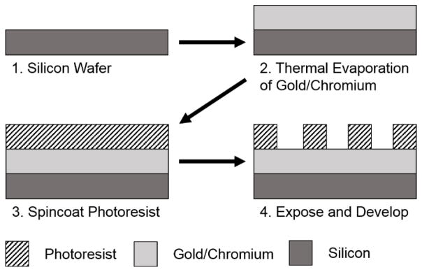
Massive electrochemical arrays containing up to 110,000 uniform circular gold UMEs were fabricated using standard photolithography techniques and the process is illustrated in Scheme 1. The use of silicon-based microfabrication facilities ensures that massive UME arrays can be batch prepared with high reproducibility and fidelity. For example, the process used in this work allows us to prepare >200 nearly identical UME arrays on a 4-inch silicon wafer. The actual diameter of the electrodes in the array is about 10% smaller than they are nominally. When optimizing the exposure conditions, small unwanted features were observed in the photoresist between adjacent electrodes that were likely generated from over exposure. This is explained by the close spacing of electrodes in the mask leading to increased exposure of the photoresist between the neighboring electrodes. The exposure dosage was further lowered until these unwanted features disappeared and the electrodes became circular, which also resulted in decreased size of the electrodes. A 1-μm electrode spacing was used for all the arrays fabricated in this work. However, if a new mask is designed with more spacing between electrodes, these inter-electrode artifacts will disappear. The decrease in electrode size does not cause any difference in the faradaic current at the scan rates used in this study due to strong overlap in the diffusion layer at adjacent electrodes.
Scheme 1.
Fabrication of massive electrochemical arrays
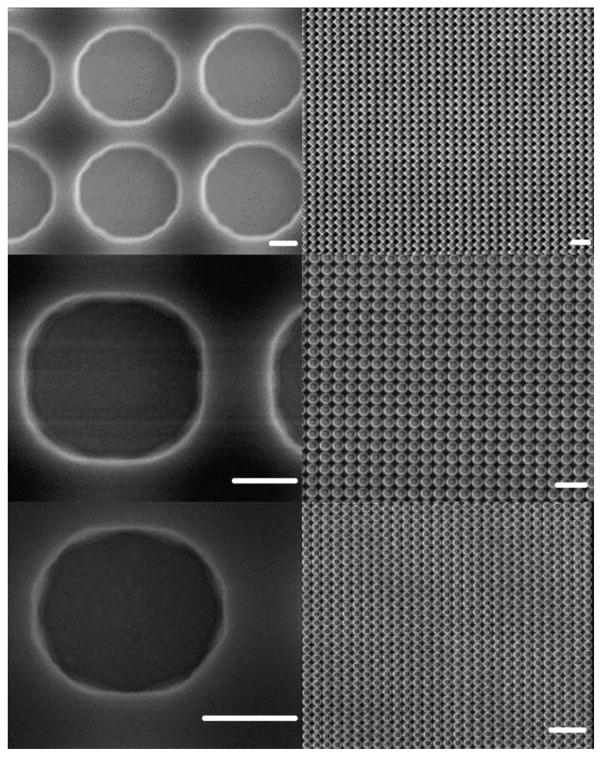
Figure 1 displays SEM images of microfabricated electrochemical arrays having 4, 3, and 2 μm electrodes (from top to bottom). The images on the right are zoom out view of the same arrays on the left. The SEM images in Figure 1 clearly demonstrate the exceedingly high uniformity of electrodes made in this work. One can see that the UMEs fabricated in each array have nearly identical size and shape over large areas (1 × 1 mm2). Individual gold UMEs are defined by a thin layer of AZ 1512 photoresist spin-coated on the gold film. The film thickness was around 1.2 μm which gives slightly recessed geometry to the gold electrodes in the array. The spacing between adjacent UMEs was 1 μm for all the arrays in Figure 1.
Figure 1.
SEM images of (from top to bottom) 4, 3, and 2 μm electrodes in the arrays. The right panel is zoomed out from the left panel. Scale bars on the left side images are 1 μm and scale bars on the right side images are 10 μm.
For our electrochemical experiments, it is important to ensure that the photoresist polymer layer adheres strongly to the gold substrate and there is no leakage current or crosstalk between adjacent electrodes. The AZ 1512 photoresist is a general purpose photoresist designed with stability in mind and its stability is well characterized and is stable in most aqueous solutions. The exception to this is in extremely basic solutions (in which photoresist is typically developed) and in solutions of oxidizing acids. This stability can be enhanced through crosslinking the photoresist polymers at elevated temperatures of 120 °C or higher. As is shown below, our tests demonstrated that the use of AZ 1512 forms a leak free and stable insulating layers in the UME arrays. In fact we tested the stability of our arrays in a solution of 1.8 M sulfuric acid, an oxidizing acid, during the deposition of copper.
We have carried out two separate experiments to test the adhesion strength of the polymer to the gold surface. In the first test experiment, we deposited metal on each UME and microscopically checked for possible deposition at areas initially covered by photoresist. The use of metal deposition is an important procedure to examine electrochemical activity on microstructures such as graphene and carbon nanotubes.34,35 Here, we electrochemically deposited cupper onto gold UMEs in the array, dissolved the polymer layer, and imaged the resulting gold surface with SEM.
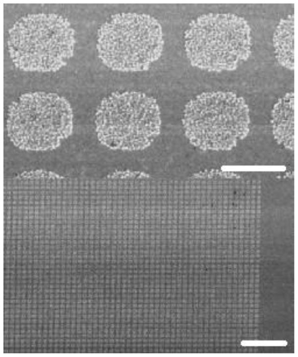
The UME arrays were examined with SEM after copper deposition and removal of the photoresist with acetone. Figure 2 shows an SEM of the 4 μm UME array after copper deposition. Copper was electrochemically deposited into the slightly recessed electrodes of the array from a 0.24 M CuSO4 solution containing 1.8 M H2SO4 by scanning the electrode potential between 0 and −0.2 V using a copper wire as the counter electrode. As one can see from Figure 2, copper was deposited uniformly on the electrodes covering the entire gold surface in the exposed areas. One can see that nanoparticles of copper were formed and evenly distributed on the surface of gold electrode during the electrodeposition process. Importantly, copper metal can only be found on the initially exposed gold but not on the polymer-covered areas indicating excellent adhesion property of photoresist on gold. Moreover, no inactive electrodes could be identified over large areas on the array. The copper electrodeposition demonstrates that nearly 100% of the electrodes in the array are active. This is important because one did not need to compensate for the inactivity of electrodes within the array during quantitative analysis of their electrochemical response and numerical simulation as every electrode that we inspected after copper electrodeposition contained uniform copper. The results shown in Figure 2 demonstrate that the photoresist indeed insulates the inter-electrode volume.
Figure 2.
Copper deposited onto the UMEs of a 4-μm array. The photoresist has been stripped with acetone. The bottom image is zoomed out from the top image to show the uniformity of deposition across the array as well as electrode activity. Scale bar is 4 μm in top image and 40 μm in bottom image.
In a second experiment, we examined the capacitive charging current for the different sized electrode arrays to further test polymer adhesion. The capacitive charging current is proportional mainly to the area of electroactive surface exposed,36
| [1] |
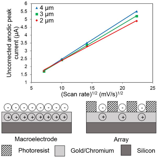
where ic is the charging current, Cdl is the double layer capacitance, and ν is the voltammetric scan rate (mV/s). To find the fraction of electrode surface area relative to total array area, we divide the total area electrode area by the geometric area of the array. The percent of electrode area exposed is 35%, 44%, and 50% for the 2 μm, 3 μm, and 4 μm electrode diameter arrays, respectively. When the uncorrected peak heights are plotted versus scan rate, as shown in Figure 3, the larger capacitive current for the larger exposed fraction arrays is apparent. In addition, the measured charging currents on these MEA arrays are comparable to that estimated based on their exposed area and the charging current measured on a 1-mm diameter gold macroelectrode in similar conditions.
Figure 3.
(Top) Uncorrected anodic peak current of the UME arrays in 1 mM FcMeOH and 100 mM KCl plotted against the square root of scan rate to show the additional capacitive current seen in arrays with a larger fraction of metal exposed. (Bottom) Illustration of the difference in capacitive current between a macroelectrode and an array of equivalent area.
3.2 Cyclic Voltammetric Response
Peak-shaped voltammograms were observed at the scan rates used because of heavily overlapping diffusions layers leading to a planar diffusion of redox molecules from bulk to the surface of the array. Peak-shaped CVs were expected considering the small spacing of the arrays, which is smaller than the diffusion layer thickness estimated based on the scan rates used in this work. For example, the diffusion thickness can be estimated according to the following equation,
| [2] |
Where δ (cm) is the thickness of the diffusion layer, D (cm2/s) is the diffusion coefficient for the redox molecule, and τ is the characteristic time duration of the voltammetric experiment and is estimated from RT/νF, where R is the gas constant, and T is temperature, and F is the Faraday’s constant. The estimated τ is 2.6 s assuming a scan rate of 10 mV/s and the estimated diffusion layer thickness is 112 μm (assuming typical diffusion coefficient of 10−5 cm2/s and T = 298 K). Since δ = 112 μm is much greater than the 1 μm electrode spacing, there is significant overlapping of diffusion layer between adjacent electrodes in the array leading to the peak-shaped voltammetric response.
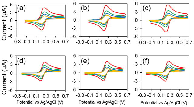
Figures 4a–c show a series of CVs taken at 4 different scan rates, 50 mV/s (yellow), 100 mV/s (blue), 200 mV/s (green), and 500 mV/s (red), from three different arrays (a) 2 μm, (b) 3 μm, and (c) 4 μm in 1 mM FcMeOH and 100 mM KCl. The scan rates used were in order from lowest to highest anodic peak current. Nearly ideal peak-shaped CVs were obtained for all three different arrays and the peak separations were between 65 and 70 mV for each array. The shape of the CV and the small peak separation both indicate excellent voltammetric performance and confirmed the planar diffusion resulting from strong diffusion overlap. Importantly, all the arrays had similar corrected peak currents (Figure 6a). This is expected as the geometric area of the array determines the total faradaic current assuming that diffusion layers overlap sufficiently. It is also noteworthy that even at an edge-to-edge spacing of 1 μm the photoresist adheres well and we obtain the capacitive current expected of an array. The arrays were meticulously cleaned with piranha solution as previously described and care was taken to not contaminate the gold surface afterward. Interestingly, the peak separation became smaller at higher scan rates, suggesting stronger contribution from FcMeOH molecules either trapped in the shallow polymer recess or adsorbed to the gold electrodes. One can anticipate that the voltammetric response will slowly transit to a thin-layer type response when scan rate is further increased similar to that observed for a glass nanopore electrode.37,38
Figure 4.
Experimental CVs of the (a) 2 μm, (b) 3 μm, and (c) 4 μm arrays in 1 mM FcMeOH and 100 mM KCl. (d–f) Simulated CVs of the (d) 2 μm, (e) 3 μm, and (f) 4 μm arrays in 1 mM FcMeOH using a 2D geometry. The scan rates used are 50 mV/s, 100 mV/s, 200 mV/s, and 500 mV/s in order from lowest to highest anodic peak current.
Figure 6.
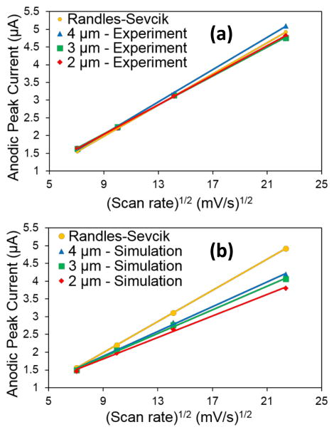
(a) Experimental and (b) simulated CV peak currents of arrays in 1 mM FcMeOH and 100 mM KCl. Scan rates are 50 mV/s, 100 mV/s, 200 mV/s, and 500 mV/s.
We also compared our CV peak heights in Figures 4a–c with those predicted by the Randles-Ševčík equation,39,40
| [3] |
where n is the number of electrons transferred, A is the geometric area of the electrode, C is the concentration of redox molecule, and with other parameters previously defined. After correcting for capacitive charging current, the experimental CVs agree with the Randles-Ševčík prediction to within 5% for all arrays and scan rates. Some of this difference may be partly due to the use of the Randles-Ševčík equation for a disc electrode whereas our array geometry is square and the electrodes are slightly recessed.
3.3 Numerical Simulation
The electrochemical response of the 2 μm UME arrays was first simulated in a 2D geometry using the diffusion domain approximation as well as a 3D geometry. The diffusion domain approximation secludes each electrode in the array into its own diffusion volume.9 This single electrode and its volume were then simulated and the resulting voltammetric response was multiplied by the number of electrodes in the array. The difference in peak current height between the 2D and 3D simulations at all scan rates for the 2 μm simulations was less than 2%. All subsequent simulations were performed as 2D simulations. The 2D and 3D simulation geometries are shown in Figure 5.
Figure 5.
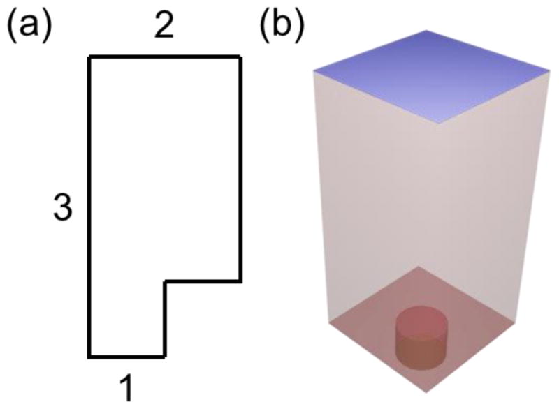
Simulated geometries. (a) Simulated 2D geometry. Side 1 is the time dependent concentration equation, side 2 is the bulk concentration Cb, and side 3 is the axis of rotational symmetry. All other sides are insulators with no flux. Not drawn to scale (b) Core electrode. The top blue side is the bulk concentration Cb, the disk at the bottom of the well is the time dependent concentration equation, all other red sides are insulators with no flux. Not drawn to scale.
The electrochemical reaction was modeled as a one electron oxidation of R → O + e− occurring at a potential of E0 = 0.23 V. Convection and migration were assumed to be insignificant compared to diffusion due to the presence of a large concentration of supporting electrolyte. The diffusion coefficient of the reduced and oxidized species of FcMeOH was assumed to be the same and was used as D = 6.7 × 10⁻⁶ cm2 s−1.41 The potential waveform was modeled as a step-wise triangle function with a starting potential of −0.2 V, a switching potential of 0.6 V, and a frequency that was dependent on the scan rate v. The simulation was run for one period of this waveform. The boundary condition at the electrode was
| [4] |
as previously described elsewhere41 where CR is the concentration of the reduced redox molecule, Cb is the bulk concentration, E(t) is the step-wise triangle waveform described previously, and other parameters were previously defined.
Side 1 in Figure 5a is the electrode with a length equal to the radius of the electrode, either 1 μm, 1.5 μm, or 2 μm. This electrode is recessed by 1.2 μm, the thickness of the spun photoresist. This recessed electrode is placed into a confined diffusion volume. Side 1 has a boundary condition of the time dependent concentration as described in Eq. 1. Side 2 has a length equal to the radius of the electrode plus half a micrometer to simulate the individual diffusion volume of that electrode. Side 2 has the boundary condition of bulk concentration. Side 3 is the axis of the symmetry and has a length equal to the recess and an additional 1 mm to simulate the height of the drop of solution placed onto the array. All other sides in the 2D geometry have a boundary condition of no flux. In Figure 5b the 3D geometry has a boundary condition at the blue top of bulk concentration. The time dependent concentration Eq.1 is the boundary condition at the electrode surface at the bottom of the well. All other sides have the boundary condition of no flux.
Figures 4d–f are simulated CVs of the arrays in 1 mM FcMeOH using a 2D geometry. One can see that the simulation CVs are also peak-shaped and the shape matched quite well with the experimental CVs. Figure 6 shows a comparison of the experimental and simulated CV peak currents of all the arrays in 1 mM FcMeOH and 100 mM KCl at all four scan rates. Simulated peak heights show excellent agreement with experiment and prediction from the Randles-Ševčík equation at low scan rates but fall to ~75% of the theoretical and experimental values at 500 mV/s which suggests a shortcoming of the simulation method. Since the simulated currents are below the experimental, it is possible that the difference in redox current is due to underestimated redox flux at the edge electrodes. However, the exact reasons are still being investigated.
4. Conclusion
In summary, we have demonstrated the fabrication and voltammetric characterization of massive electrochemical arrays containing as many as 110,000 uniform ultramicroelectrodes. The photolithography-based fabrication method employed in this work is simple, fast, and reliable. Electrode size, shape, and spacing can be systematically varied to generate massive electrochemical arrays with controlled geometry. All electrodes examined were found to be active through copper electrodeposition. Voltammetric response of such arrays was found to be dominated by a planar diffusion resulting from heavily overlapping diffusion profiles of nearly electrodes. Their CVs have peak currents that matched very closely with the prediction using Randles-Ševčík equation. The voltammetric response was further verified by numerical simulation and the simulation matched well with the experimental at slow scan rates. The larger difference at higher scan rates were likely due to increasing edge effects and the details will be investigated in the future. This method should prove useful in creating uniform, active, and massive arrays of microelectrodes of any geometry for electroanalytical studies.
Acknowledgments
We gratefully thank financial support from the National Science Foundation (CHE-1515897) and National Institutes of Health (GM101133). We also thank Stephen Percival for creating the microarray photomask and Duane Irish and Andrew Lingley of the Washington Nanofabrication Facility for help with photolithography.
Footnotes
Dedicated to Prof. Hongyuan Chen for his 80th birthday.
Publisher's Disclaimer: This is a PDF file of an unedited manuscript that has been accepted for publication. As a service to our customers we are providing this early version of the manuscript. The manuscript will undergo copyediting, typesetting, and review of the resulting proof before it is published in its final citable form. Please note that during the production process errors may be discovered which could affect the content, and all legal disclaimers that apply to the journal pertain.
References
- 1.Oja SM, Fan Y, Armstrong CM, Defnet P, Zhang B. Nanoscale electrochemistry revisited. Anal Chem. 2016;88:414–430. doi: 10.1021/acs.analchem.5b04542. [DOI] [PubMed] [Google Scholar]
- 2.Arrigan DW. Nanoelectrodes, nanoelectrode arrays and their applications. Analyst. 2004;129:1157–1165. doi: 10.1039/b415395m. [DOI] [PubMed] [Google Scholar]
- 3.Penner RM, Martin CR. Preparation and electrochemical characterization of ultramicroelectrode ensembles. Anal Chem. 1987;59:2625–2630. [Google Scholar]
- 4.Rieger PH. Electrochemistry. Chapman & Hall, Inc; New York: 1994. pp. 215–223. [Google Scholar]
- 5.Heinze J. Ultramicroelectrodes in electrochemistry. Angew Chem Int Ed Engl. 1993;32:1268–1288. [Google Scholar]
- 6.Watkins JJ, Chen J, White HS, Abruña HD, Maisonhaute E, Amatore C. Zeptomole voltammetric detection and electron-transfer rate measurements using platinum electrodes of nanometer dimensions. Anal Chem. 2003;75:3962–3971. doi: 10.1021/ac0342931. [DOI] [PubMed] [Google Scholar]
- 7.Mirkin MV, Bard AJ. Simple analysis of quasi-reversible steady-state voltammograms. Anal Chem. 1992;64:2293–2302. [Google Scholar]
- 8.Howell JO, Wightman RM. Ultrafast voltammetry and voltammetry in highly resistive solution with microvoltammetric electrodes. Anal Chem. 1984;56:524–529. [Google Scholar]
- 9.Amatore C, Deakin MR, Wightman RM. Electrochemical kinetics at microelectrodes: Part IV. Electrochemistry in media of low ionic strength. J Electroanal Chem. 1987;220:49–63. [Google Scholar]
- 10.Oldham KB. Theory of steady-state voltammetry without supporting electrolyte. J Electroanal Chem. 1992;337:91–126. [Google Scholar]
- 11.Andrieux CP, Garreau D, Hapiot P, Savéant JM. Ultramicroelectrodes: cyclic voltammetry above one million v s−1. J Electroanal Chem. 1988;248:447–450. [Google Scholar]
- 12.Amatore C, Maisonhaute E. When voltammetry reaches nanoseconds. Anal Chem. 2005;77:305A–311A. doi: 10.1021/ac053430m. [DOI] [PubMed] [Google Scholar]
- 13.Penner RM, Martin CR. Preparation and electrochemical characterization of ultramicroelectrodes ensembles. Anal Chem. 1987;59:2625–2630. [Google Scholar]
- 14.Amatore C, Savéant JM, Tessier D. Charge transfer at partially blocked surfaces: A model for the case of microscopic active and inactive sites. J Electroanal Chem. 1983;147:39–51. [Google Scholar]
- 15.Davies TJ, Ward-Jones S, Banks CE, del Campo J, Mas R, Muñoz FX, Compton RG. The cyclic and linear sweep voltammetry of regular arrays of microdisc electrodes: fitting of experimental data. J Electroanal Chem. 2005;585:51–62. [Google Scholar]
- 16.Menon VP, Martin CR. Fabrication and evaluation of nanoelectrode. Anal Chem. 1995;67:1920–1928. [Google Scholar]
- 17.Moretto LM, Pepe N, Ugo P. Voltammetry of redox analytes at trace concentrations with nanoelectrode ensembles. Talanta. 2004;62:1055–1060. doi: 10.1016/j.talanta.2003.10.024. [DOI] [PubMed] [Google Scholar]
- 18.Ugo P, Pepe N, Moretto LM, Battagliarin M. Direct voltammetry of cytochrome C at trace concentrations with nanoelectrode ensembles. J Electroanal Chem. 2003;560:51–58. [Google Scholar]
- 19.Feeney R, Kounaves SP. On-site analysis of arsenic in groundwater using a microfabricated gold ultramicroelectrode array. Anal Chem. 2000;72:2222–2228. doi: 10.1021/ac991185z. [DOI] [PubMed] [Google Scholar]
- 20.Jena BK, Raj CR. Gold nanoelectrode ensembles for the simultaneous electrochemical detection of ultratrace arsenic, mercury, and copper. Anal Chem. 2008;80:4836–4844. doi: 10.1021/ac071064w. [DOI] [PubMed] [Google Scholar]
- 21.Abe H, Ino K, Li CZ, Kanno Y, Inoue KY, Suda A, Kunikata R, Matsudaira M, Takahashi Y, Shiku H, Matsue T. Electrochemical imaging of dopamine release from three-dimensional-cultured PC12 cells using large-scale integration-based amperometric sensors. Anal Chem. 2015;87:6364–6370. doi: 10.1021/acs.analchem.5b01307. [DOI] [PubMed] [Google Scholar]
- 22.Zhang B, Adams KL, Luber SJ, Eves DJ, Heien ML, Ewing AG. Spatially and temporally resolved single-cell exocytosis utilizing individually addressable carbon microelectrode arrays. Anal Chem. 2008;80:1394–1400. doi: 10.1021/ac702409s. [DOI] [PMC free article] [PubMed] [Google Scholar]
- 23.Wang J, Trouillon R, Lin Y, Svensson MI, Ewing AG. Individually addressable thin-film ultramicroelectrode array for spatial measurements of single vesicle release. Anal Chem. 2013;85:5600–5608. doi: 10.1021/ac4009385. [DOI] [PubMed] [Google Scholar]
- 24.Wang J, Ewing AG. Simultaneous study of subcellular exocytosis with individually addressable multiple microelectrodes. Analyst. 2014;139:3290–3295. doi: 10.1039/c4an00058g. [DOI] [PubMed] [Google Scholar]
- 25.Hafez I, Kisler K, Berberian K, Dernick G, Valero V, Yong MG, Craighead HG, Lindau M. Electrochemical imaging of fusion pore openings by electrochemical detector arrays. Proc Natl Acad Sci U S A. 2005;102:13879–13884. doi: 10.1073/pnas.0504098102. [DOI] [PMC free article] [PubMed] [Google Scholar]
- 26.Gosso S, Turturici M, Franchino C, Colombo E, Pasquarelli A, Carbone E, Carabelli V. Heterogeneous distribution of exocytotic microdomains in adrenal chromaffin cells resolved by high-density diamond ultra-microelectrode arrays. J Physiol. 2014;592:3215–3230. doi: 10.1113/jphysiol.2014.274951. [DOI] [PMC free article] [PubMed] [Google Scholar]
- 27.Wigström J, Dunevall J, Najafinobar N, Lovrić J, Wang J, Ewing AG, Cans AS. Lithographic microfabrication of a 16-electrode array on a probe tip for high spatial resolution electrochemical localization of exocytosis. Anal Chem. 2016;88:2080–2087. doi: 10.1021/acs.analchem.5b03316. [DOI] [PubMed] [Google Scholar]
- 28.Nam Y, Chang JC, Wheeler BC, Brewer GJ. Gold-coated microelectrode array with thiol linked self-assembled monolayers for engineering neuronal cultures. IEEE Trans Biomed Eng. 2004;51:158–165. doi: 10.1109/TBME.2003.820336. [DOI] [PubMed] [Google Scholar]
- 29.Menshykau D, Huang XJ, Rees NV, del Campo FJ, Muñoz FX, Compton RG. Investigating the concept of diffusional independence. Potential step transients at nano- and micro-electrode arrays: theory and experiment. Analyst. 2009;134:343–348. doi: 10.1039/b816223a. [DOI] [PubMed] [Google Scholar]
- 30.Huang XJ, O’Mahony AM, Compton RG. Microelectrode arrays for electrochemistry: approaches to fabrication. Small. 2009;5:776–788. doi: 10.1002/smll.200801593. [DOI] [PubMed] [Google Scholar]
- 31.Lesch A, Momotenko D, Cortés-Salazar F, Wirth I, Tefashe UM, Meiners F, Vaske B, Girault HH, Wittstock G. Fabrication of soft gold microelectrode arrays as probes for scanning electrochemical microscopy. J Electroanal Chem. 2012;666:52–61. [Google Scholar]
- 32.Lima AEB, Luz GE, Batista NC, Longo E, Cavalcante LS, Santos RS. Determination of Ethambutol in Aqueous Medium Using an Inexpensive Gold Microelectrode Array as Amperometric Sensor. Electroanal. 2015;28:985–989. [Google Scholar]
- 33.Spira ME, Hai A. Multi-electrode array technologies for neuroscience and cardiology. Nat Nanotechnol. 2013;8:83–94. doi: 10.1038/nnano.2012.265. [DOI] [PubMed] [Google Scholar]
- 34.Day TM, Unwin PR, Macpherson JV. Factors Controlling the Electrodeposition of Metal Nanoparticles on Pristine Single Walled Carbon Nanotubes. Nano Lett. 2007;7:51–57. doi: 10.1021/nl061974d. [DOI] [PubMed] [Google Scholar]
- 35.Quinn BM, Dekker C, Lemay SG. Electrodeposition of noble metal nanoparticles on carbon nanotubes. J Am Chem Soc. 2005;127:6146–6147. doi: 10.1021/ja0508828. [DOI] [PubMed] [Google Scholar]
- 36.Bard AJ, Faulkner LR. Electrochemical Methods. 2. John Wiley & Sons; New York: 2001. [Google Scholar]
- 37.Zhang B, Zhang Y, White HS. The nanopore electrode. Anal Chem. 2004;76:6229–6438. doi: 10.1021/ac049288r. [DOI] [PubMed] [Google Scholar]
- 38.Zhang B, Zhang Y, White HS. Steady-State Voltammetric Response of the Nanopore Electrode. Anal Chem. 2006;78:477–483. doi: 10.1021/ac051330a. [DOI] [PubMed] [Google Scholar]
- 39.Randles JEB. A cathode ray polarography. Trans Faraday Soc. 1948;44:322–327. [Google Scholar]
- 40.Ševčík A. Oscillographic polarography with periodical triangular voltage. Collect Czech Chem Commun. 1948;13:349–377. [Google Scholar]
- 41.Guerrette JP, Percival SJ, Zhang B. Voltammetric Behavior of Gold Nanotrench Electrodes. Langmuir. 2011;27:12218–12225. doi: 10.1021/la2023743. [DOI] [PubMed] [Google Scholar]


