

Atomic engineering of donor-based spin qubits results in long lifetimes and high-fidelity two-qubit readout.
Keywords: donors, silicon, scanning tunnelling microscopy, Quantum Computation, electron spin, spin relaxation, readout
Abstract
Scaling up to large arrays of donor-based spin qubits for quantum computation will require the ability to perform high-fidelity readout of multiple individual spin qubits. Recent experiments have shown that the limiting factor for high-fidelity readout of many qubits is the lifetime of the electron spin. We demonstrate the longest reported lifetimes (up to 30 s) of any electron spin qubit in a nanoelectronic device. By atomic-level engineering of the electron wave function within phosphorus atom quantum dots, we can minimize spin relaxation in agreement with recent theoretical predictions. These lifetimes allow us to demonstrate the sequential readout of two electron spin qubits with fidelities as high as 99.8%, which is above the surface code fault-tolerant threshold. This work paves the way for future experiments on multiqubit systems using donors in silicon.
INTRODUCTION
The initialization, readout, and manipulation of electron spins bound to a single phosphorus (P) donor in silicon have been demonstrated with fidelities more than 99% (1, 2), which is above the estimated threshold for surface code quantum error correction (3, 4), making them a promising qubit for quantum computation (5, 6) and simulation (7). One of the main sources of error during single-shot spin readout is the relaxation of the spins before they can be measured (8). The spin relaxation time (T1) also represents an upper bound to the spin coherence times (T2 < 2T1) (9). Consequently, extensive efforts have been made to understand the underlying mechanisms that cause spin relaxation to extend the lifetimes of electron spin qubits (10–12).
The relaxation times of electrons bound to P donors in silicon are particularly long because of weak spin-orbit coupling and the lack of piezoelectric phonons (9). In these systems, relaxation is caused by the single-valley and valley repopulation mechanisms, which depend on the valley-orbit splitting (13, 14). Here, we show that electrons bound to 2P and 3P donor dots can have spin relaxation times up to 16 times longer than single P donors because of their extremely tight confinement potential, which results in a larger valley-orbit splitting, in agreement with recent theoretical predictions (13). These long spin relaxation times, combined with a single-electron transistor (SET) charge sensor that has a high signal-to-noise ratio, allow us to demonstrate the high-fidelity (99.8%) sequential readout of two donor-bound electron spin qubits.
RESULTS
An overview of the device after scanning tunneling microscope (STM) hydrogen lithography (15, 16) is shown in Fig. 1A. Two atomic-scale quantum dots, D1 and D2, are placed at a center-to-center distance of 20 nm apart and at a distance of ~19 nm from the SET charge sensor. Four in-plane gates—G1, G2, GSET, and GT—are used to tune the electrochemical potentials of the dots and the SET island. Dosing with PH3 followed by annealing (350°C) creates an atomically abrupt planar doping profile with density N2D ≈ 2 × 10¹⁸ m−2 (16, 17), where we estimated a maximum of three donors to be incorporated in D1 and D2 from the STM images in Fig. 1 (B and C, respectively) (15, 18).
Fig. 1. Charge sensor for independent readout of two P donor quantum dots.
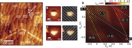
(A) Overview STM image of the device template after STM lithography showing four electrostatic gates (G1, G2, GT, and GSET) and a SET charge sensor with source (S) and drain (D) leads. Two donor incorporation sites, D1 and D2 separated by 20 nm, were patterned 19 nm away from the SET. (B and C) Closeup STM images of D1 and D2 with the underlying Si(001)-(2 × 1) surface reconstruction. Both dot templates consist of three and four contiguous desorbed dimers (green ellipses) along two adjacent dimer rows. Assuming a 0.25–monolayer (ML) doping density (31), we estimate that a maximum of three P can be incorporated in D1 and D2. (D) Charge stability diagram (VSD = 300 μV, VGT = 100 mV, and VGSET = 0 mV) showing the current through the SET as a function of the voltage applied to G1 and G2. We observe two sets of parallel lines of breaks in the SET current where either the D1 (yellow dashed lines) or D2 (blue dashed lines) electrochemical potentials align with that of the SET.
The charge sensing and independent gate control (8) of the double quantum dot (DQD) are demonstrated in Fig. 1D, which shows the SET current as a function of the gate voltages VG1 and VG2, recorded at voltages VSD = 300 μV, VGT = 100 mV, and VGSET = 0 mV. Lines of current running at 45° correspond to the Coulomb blockade (CB) peaks of the SET. Charge transitions on D1 and D2 result in two sets of parallel lines of charge offsets in the CB pattern (blue and yellow dashed lines), which connect to form a honeycomb diagram expected for the DQD (19). No additional charge transitions for D1 and D2 are observed for voltages V < 0 V, indicating that both dots can be fully depleted, allowing us to assign the electron occupancy (m, n) to each charge stable region shown in Fig. 1D. Because a single P donor can only bind up to two electrons (18), the observation that each dot has more than two charge transitions (see section S1) indicates that each dot hosts more than one single P donor.
The donor numbers of D1 and D2 can be estimated by comparing their addition energies with those calculated using an atomistic tight-binding model (see section S1) (15) and were found to be 3P and 2P, respectively. The addition energies for the 1e↔2e and 2e↔3e transitions of D1 (108 ± 15 meV and 78 ± 12 meV) and D2 (63 ± 9 meV and 61 ± 11 meV) were extracted by measuring the change in voltage between successive charge transitions of D1 (D2) and converting to an energy with extracted gate lever arms. The addition energies of D1 are significantly larger than D2, indicating a stronger confinement potential due to the higher donor number.
A key requirement to demonstrate a successful two-qubit logic gate is the ability to independently read out and initialize each qubit (20). Figure 2A shows a high-resolution close-up of the (0,0)↔(1,1) charge transition where the sequential readout by spin-selective tunneling of each electron to the SET island (21) was performed. In this map, we observed almost no charge offset drift (22), allowing us to maintain readout without feedback over days. The white dashed lines outline the charge stable regions of the DQD. Adding an electron to either of the dots shifts the SET peak by more than its linewidth, resulting in excellent sensitivity to the tunneling of electrons from D1 and D2. To read out D1 (D2), we applied a static magnetic field, B, which splits the spin-degenerate, one-electron ground state into spin-up |↑〉 and spin-down |↓〉, separated by the Zeeman energy ΔEZ = gμBB. The electrochemical potential of the SET is aligned between the |↑〉 and |↓〉 electrochemical potentials of D1 (D2). If the electron spin is in the |↑〉 state, then it will tunnel onto the SET island, followed by a |↓〉 returning to the donor dot, resulting in a single pulse in the SET current. The readout position for D1 (D2) with 0e or 1e on D2 (D1) in gate-gate space is shown in Fig. 2A (red and blue stars and circles). The position of the SET lines could be tuned with respect to the charge stable regions of the DQD (defined by white dashed lines) using GT and GSET and were chosen to bring the readout positions of both dots close together in gate space. From the variation in the addition energy spectrum of the SET measured in Fig. 2A, we estimated an upper bound for the single-level energy spacing of the SET to be ΔE < 40 μeV ≪ EZ, allowing us to treat the SET as a reservoir with a continuum of states (23). For this large, donor-based SET (A ~ 1000 nm2), we found that a simple two-dimensional particle-in-a-box model does not accurately predict ΔE, which is most likely because of the asymmetry and disorder in the confinement potential and the many thousands of electrons (estimated from the 0.25-ML doping density), which will lead to complicated electron-electron correlations.
Fig. 2. Extending T1 using single electron spins bound to multidonor quantum dots.
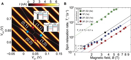
(A) Measured charge stability diagram showing the positions in gate space where readout is performed on D1 and D2, recorded at VSD = 1.5 mV, VGT = −200 mV, and VGSET = 20 mV. The red and blue stars (circles) are the readout positions for D1 and D2 if the other dot is unoccupied (occupied). (B) Measured spin relaxation rates, T1−1, of the first electron bound to D1 (red squares) and D2 (blue squares) and the third electron bound to D2 (green squares) as a function of magnetic field. The data follow T1−1 = K5B5 with K5 = 0.00059 ± 0.00002 s−1 T−5, K5 = 0.0028 ± 0.0001 s−1 T−5, and K5 = 1.3 ± 0.1 s−1 T−5 for D1 (1e), D2 (1e), and D2 (3e), respectively. The black line shows the fit (K5 = 0.0095 s−1 T−5) to the spin relaxation times of the single donor device in the study by Watson et al. (2) measured at the same magnetic field direction used in this experiment.
The relaxation time T1 of an electron spin qubit determines the fundamental limit of the qubit coherence time (T2 < 2T1) and is important to determine the readout fidelity. We measured the spin relaxation time of the first electron bound to D1 (D2) while the other donor dot is unoccupied by applying a three-level pulse sequence. In this sequence, D1 (D2) is first emptied by pulsing with G1 and G2 into the (0,0) charge region. D1 or D2 is then loaded with a random spin by pulsing deep into either the (1,0) or (0,1) charge region. After waiting a time twait, the electron spin of D1 (D2) is read out by pulsing to the red and blue stars in Fig. 2A. The |↑〉 fraction decays exponentially as a function of twait, allowing us to extract the T1 of D1 and D2 at various magnetic fields. Figure 2B shows the spin relaxation rates T1−1 of the 2P (D2) (blue squares) and 3P (D1) (red squares) donor dots as a function of a magnetic field applied at 68° ± 2° with respect to the [100] crystalline axis (see Fig. 1A). Note that we observed no change in the spin relaxation times if an extra electron is added to the other dot. For magnetic fields B ≥ 3 T, the spin relaxation rates follow a B5 field dependence, as expected for donors in silicon where the single-phonon mechanisms of valley repopulation and the single-valley mechanism are the dominant relaxation pathways (14, 24, 25). For lower magnetic fields below ~3 T, the spin relaxation rate of both dots deviates from the B5 field dependence, suggesting that another spin relaxation mechanism dominates. Similar behavior has been observed in previous experiments on donors in silicon (2, 24–26), where there is evidence for a change in slope at low magnetic fields where the spin relaxation times are between 0.2 and 5 s (see section S3 for comparison). In our experiment, we observed that the spin relaxation rate first saturates and then decreases with a different slope from the B5 field dependence at lower B. In the study by Morello et al. (24), the deviation from the B5 field dependence was explained by a B field–independent relaxation mechanism involving the dipolar coupling between the measured electron spin and nearby donor electron spins. However, it could be argued that the data does not become B field–independent at lower magnetic fields and is similar to the data shown in Fig. 2B. In quantum dots, similar deviations at low B fields have been predicted theoretically to arise from unfiltered Johnson noise from the finite resistance of the device reservoirs or gates (~1 kilohm), causing relaxation via Rashba spin-orbit coupling, which leads to a B3 field dependence (27). This behavior would also be expected in donors, particularly in asymmetric confining potentials, which may arise from multiple donors or electrostatic gates.
The black line in Fig. 2B shows the spin relaxation rate of the single donor device in the study by Watson et al. (2) as a function of magnetic field extrapolated from a data point measured using the same magnetic field direction used in this experiment. The relaxation time of the electrons increases significantly for dots with higher donor numbers, and we found that the spin relaxation times for the 3P donor dot are 16 times longer than for the single P donor. This is in qualitative agreement with recent theoretical predictions based on an atomistic tight-binding model (13), where dots with higher donor numbers have a stronger confinement potential for the first bound electron. This tighter confinement potential reduces the electron wave function overlap with the lattice and results in a larger valley-orbit energy gap, combining to reduce the phonon-induced relaxation. Significantly, at a magnetic field of B = 1.5 T, we found T1 times of T1 = 30 s and T1 = 15 s for D1 and D2, respectively, which are the longest reported spin relaxation times for any single electron spin qubit in a nanoelectronic device.
It is expected that, as we add more electrons to these tightly confined systems, the relaxation time of an unpaired electron spin should markedly increase because of screening of the donor core potential (13). This increases the spread in the electron wave function increasing T1. We observed this change for the third electron bound to D2 that is shown in Fig. 2B (green squares), continuing the trend of decreasing spin lifetimes with increasing confinement size as predicted by theory. The spin relaxation rate also follows a B5 field dependence but is about three orders of magnitude faster than the first electron from the same dot. The ability to perform readout of the third electron bound to D2 indicates even-odd spin filling, consistent with previous measurements on 2P and 3P donor dots in silicon (15). Note that, although we observed the third electron transition for D1, we could not perform spin readout because the tunnel times were too fast (<1 μs) to measure with our measurement setup, which has a maximum bandwidth of 400 kHz.
A surface code fault-tolerant quantum computer requires the ability to independently read out and initialize each qubit with fidelities >99% (3, 4). To date, readout of more than one electron spin qubit has only been demonstrated in electrostatically defined quantum dots with fidelities still below the estimated surface code fault-tolerant threshold (20, 28–30). The sequential readout of the donor dots D1 and D2 with 99.8% fidelity is demonstrated in Fig. 3A, which shows the current through the SET during 20 readout cycles. The readout was performed at a magnetic field of B = 1.5 T typical for performing single qubit gates via electron spin resonance (1). For sequential readout, we began in the (1,1) charge state and pulsed to the D1 readout position (Fig. 2A, red circle) for 200 ms, followed by the D2 readout position (Fig. 2A, blue circle) for 200 ms. The readout results in the initialization of both dots to |↓〉. From the current response at the two read positions, we can determine the spin state of both dot-bound electrons. To repeat the readout cycle, we reinitialized both donor dots with a random spin by first emptying each donor dot by pulsing into either the (0,1) or (1,0) charge region, followed by pulsing deep into the (1,1) charge region, reloading the donor dot with a random spin. At this readout point, we found that the measured spins are uncorrelated, that is, the product of the single spin probabilities on the left (PLi) and right (PRi) dots are equal to the two spin probabilities (Pij = PLi × PRi), where i,j ∈ |↓〉, |↑〉.
Fig. 3. High-fidelity sequential readout of two electron spins confined to a 3P/2P DQD.
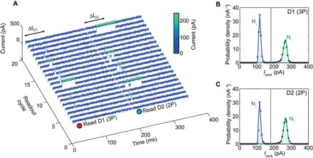
(A) Twenty readout traces showing the real-time current through the SET during the sequential single-shot readout of D1 and D2 for a magnetic field of B = 1.5 T and VSD = 170 μV. A spin-up is assigned to D1 or D2 if a current pulse occurs during the read phase. (B and C) Histograms (black circles) of the peak current during the readout of (B) D1 and (C) D2 for 7500 readout cycles. The two well-separated peaks allow |↓〉 and |↑〉 electrons to be distinguished with high fidelity. The blue and green lines show the separated histograms for the |↓〉 and |↑〉 current traces, which were simulated using the experimental parameters.
To calculate the measurement fidelity (Fm) of the sequential readout of D1 and D2, we considered the fidelity of the spin-to-charge conversion and the electrical detection separately (2). Errors during the spin-to-charge conversion arise from either (i) a |↓〉 electron tunneling out of the donor due to the thermal broadening of the SET Fermi level or (ii) a |↑〉 electron relaxing to a |↓〉 before it can tunnel out. For the readout of D1 (D2), we achieved extremely high spin-to-charge conversion fidelities for both |↓〉 (β) and |↑〉 (α) electrons above 99.9% (see section S2), which is reflected by the lack of dark counts that occur after the optimized readout time of Δt = 65 ms (55 ms). These high fidelities are results of the long spin relaxation times of the donor dots and the long |↓〉 tunnel-out time (~100 s) due to the low electron temperature (Telectron ≈ 100 mK) and the careful positioning of the readout position (see section S2). Despite kT << EZ, the |↓〉 tunnel-out time is still of a similar order of magnitude as T1, resulting in both processes contributing equally to the remaining errors in the spin-to-charge conversion.
During readout, the spin of the electron is assigned to |↑〉 if the current rises above the threshold current It determined after the experiment to maximize the measurement fidelity. Errors involved in this detection process arise from either (i) |↑〉 current pulses that are missed because of the finite bandwidth of the measurement or (ii) electrical noise resulting in a |↓〉 current pulse that is accidentally detected as a |↑〉. Figure 3 (B and C) shows histograms of the peak current, Ipeak, during the readout of D1 and D2 (black circles), which can be separated into the |↓〉 (blue line) and |↑〉 (green line) contribution, N↓ and N↑ with numerical modeling (24). The fidelity of the threshold detection scheme for D1 (D2) for a |↓〉 and |↑〉 electron can be calculated from these histograms to be F↓ = 100% (100%) and F↑ = 99.7% (99.8%), respectively (see section S2). These high fidelities can be attributed to the ability to precisely position the donor dots with respect to the SET to control the tunnel times and maximize the sensitivity of the SET to charge movement, resulting in a large signal-to-noise ratio at a measurement bandwidth of 10 kHz.
The total measurement fidelity is defined as Fm = (βF↓ + αF↑)/2 (2), giving Fm = 99.8% for D1 and Fm = 99.8% for D2, which demonstrates high-fidelity sequential single-shot readout of the electron spin bound to two donor dots above the fault-tolerant threshold. If we include the errors due to the spin relaxation of the electron bound to D1 during the readout of D2 (assuming the optimal readout time of Δt = 65 ms), then the total readout fidelity of D1 slightly reduces to Fm = 99.6%. In general, the sequential readout of the nth electron will have a readout fidelity of Fm (n) = (βF↓ + αF↑exp[−Δt × (n − 1)/T1])/2, where Δt is the average readout time for each qubit. On the basis of the numbers from this experiment, we estimated that approximately five qubits could be read out sequentially using the same charge sensor with fidelities ~99%.
DISCUSSION
The relaxation time of an electron spin qubit is important because it places an upper bound on the qubit coherence time and is one of the major contributors to measurement error. We have shown that the spin relaxation times of the first electron bound to 2P and 3P donor dots in silicon are significantly longer than in single donors (up to 30 s at B = 1.5 T), in agreement with theoretical predictions. This is due to the tighter confinement potential and larger valley-orbit splitting of the donor dots, which reduces the qubit interaction with phonons. Further insights into the exact mechanisms driving spin relaxation in these devices could be gained by measuring the anisotropy of the spin relaxation times as a function of the magnetic field orientation (14).
In addition, we have used these engineered few donor dots to demonstrate the high-fidelity (99.8%) sequential readout of two electron spins above the surface code fault-tolerant error threshold. These high fidelities are possible because of the long spin lifetimes in donor dots and the ability to use STM lithography to precisely position the dots with subnanometer accuracy with respect to a SET charge sensor enabling a high signal-to-noise ratio during the readout of both electron spins. These results lay down the foundation for performing multiqubit experiments with donors in silicon. In particular, similar devices with suitable exchange coupling between the two electron spins could be used to demonstrate the measurement and universal control of a two-qubit system, which is the next major milestone for building a scalable quantum computer with donor-based qubits.
MATERIALS AND METHODS
Device fabrication
The silicon device was fabricated using STM hydrogen lithography performed in ultrahigh vacuum (16, 18). A clean H/Si(001)-(2 × 1)–reconstructed surface was prepared by flashing the substrate to 1100°C for 1 min. The surface was passivated with hydrogen (produced by a cracker source) for 6 min at a chamber pressure of 5 × 10⁻⁷ mbar while the substrate temperature was at 340°C. The hydrogen was selectively removed from the surface by scanning the STM tip under lithographic conditions (3 to 5 V, 1 to 3 nA) to form a template, which was subsequently doped by exposing the surface to 20 Langmuir of PH3 followed by annealing at 350°C for 1 min. This results in an atomically abrupt planar doping profile with 0.25-ML density (N2D ≈ 2 × 10¹⁸ m−2) (17). In three dimensions, this corresponds to a doping density of ≈1021 cm−3, three orders of magnitude above the Mott metal-insulator transition, allowing quasi-metallic conduction in all device electrodes (16), including the SET. Finally, the device was encapsulated with a ≈40-nm epitaxial Si capping layer grown at low temperature at a rate of 8 nm/hour. The device was contacted ex situ via deposition of aluminum ohmic contacts.
Electrical measurements
All electrical measurements of the device were performed at low temperature (Tbase = 20 mK) in a 3He/4He dilution refrigerator equipped with an 8-T superconducting magnet. The electron temperature was measured to be Telectron ≈ 100 mK from the thermal broadening of the Fermi level of the SET island (see section S1). The sample was connected to a breakout box at room temperature via stainless steel coaxial cables guided through copper powder filters, which filter high-frequency (gigahertz) noise. The cables have a bandwidth greater than 2 MHz suitable for the gate pulsing and current detection used in this work.
Direct current (DC) voltages were applied to the gate and drain electrodes using Yokogawa 7651 and Stanford Research Systems SIM928 voltage sources. Alternating current (AC) voltage pulses for spin readout were applied to G1 and G2 using a Tektronix AFG320 function generator and were added to the DC voltage using a passive adder circuit, where the DC and AC voltage amplitude was divided by 5 and 50, respectively. The source electrode was grounded via a Femto DLPCA-200 variable-gain low-noise current amplifier (maximum bandwidth, 500 kHZ), which converts the source-drain current into a voltage signal. An eighth-order low-pass Bessel filter with an adjustable cutoff frequency was applied to the voltage signal using a Stanford Research Systems SIM965 analog filter. The filtered voltage signal was measured using an Agilent four-channel fast digitizing oscilloscope.
Supplementary Material
Acknowledgments
We thank H. Büch, S. Hile, and Y. Wang for useful discussions. Funding: This research was conducted by the Australian Research Council Centre of Excellence for Quantum Computation and Communication Technology (project number CE110001027), the U.S. National Security Agency, and the U.S. Army Research Office (contract number W911NF-08-1-0527). B.W. acknowledges a Discovery Early Career Researcher Award Fellowship. M.Y.S. acknowledges an Australian Research Council Laureate Fellowship. Author contributions: T.F.W. and B.W. prepared the sample, performed the measurements, and analyzed the data. M.Y.S. planned and supervised the project. All authors contributed to the interpretation of the data and preparation of the manuscript. Competing interests: M.Y.S. is Editor-in-Chief of Nature Partner Journals (NPJ) Quantum Information and receives financial benefits from the position. M.Y.S. has patents related to the described work: United States (7547648), Australia (2004266178), Japan (4855255), China (739450), India (236322), and Europe (04761155.3); United States (8580674), Australia (2008900526), Japan (2010-545327), and China (200880127837.5). The other authors declare that they have no competing interests. Data and materials availability: All data needed to evaluate the conclusions in the paper are present in the paper and/or the Supplementary Materials. Additional data related to this paper may be requested from the authors.
SUPPLEMENTARY MATERIALS
Supplementary material for this article is available at http://advances.sciencemag.org/cgi/content/full/3/3/e1602811/DC1
section S1. Extraction of the electron temperature, gate lever arms, and addition energies of D1 and D2.
section S2. Fidelity of the sequential readout of D1 and D2.
section S3. Comparison of the spin relaxation times of previous donor devices.
fig. S1. Extraction of the electron temperature and gate lever arms from the thermal broadening of the SET Fermi level.
fig. S2. Extraction of the addition energy for the second and third electrons on D2.
fig. S3. Atomistic tight-binding calculations of the addition spectrum of 2P, 3P, and 4P donor dots.
fig. S4. Extraction of the spin-dependent tunnel times during readout of D1 and D2.
fig. S5. Optimization of the readout time.
fig. S6. Electrical readout fidelity of D1 and D2.
fig. S7. Deviation from the B5 field dependence in donor devices.
table S1. Comparison of lever arms (α), addition voltages (ΔVadd), and addition energies (Eadd) of D1 and D2 for each electron transition for two different cooldowns.
REFERENCES AND NOTES
- 1.Muhonen J. T., Dehollain J. P., Laucht A., Hudson F. E., Kalra R., Sekiguchi T., Itoh K. M., Jamieson D. N., McCallum J. C., Dzurak A. S., Morello A., Storing quantum information for 30 seconds in a nanoelectronic device. Nat. Nanotechnol. 9, 986–991 (2014). [DOI] [PubMed] [Google Scholar]
- 2.Watson T. F., Weber B., House M. G., Büch H., Simmons M. Y., High-fidelity rapid initialization and read-out of an electron spin via the single donor D− charge state. Phys. Rev. Lett. 115, 166806 (2015). [DOI] [PubMed] [Google Scholar]
- 3.Raussendorf R., Harrington J., Goyal K., Topological fault-tolerance in cluster state quantum computation. New J. Phys. 9, 199 (2007). [Google Scholar]
- 4.Wang D. S., Fowler A. G., Hollenberg L. C. L., Surface code quantum computing with error rates over 1%. Phys. Rev. A 83, 020302 (2011). [Google Scholar]
- 5.Kane B. E., A silicon-based nuclear spin quantum computer. Nature 393, 133–137 (1998). [Google Scholar]
- 6.Hill C. D., Peretz E., Hile S. J., House M. G., Fuechsle M., Rogge S., Simmons M. Y., Hollenberg L. C. L., A surface code quantum computer in silicon. Sci. Adv. 1, e1500707 (2015). [DOI] [PMC free article] [PubMed] [Google Scholar]
- 7.Georgescu I. M., Ashhab S., F. Nori. Quantum simulation. Rev. Mod. Phys. 86, 153–185 (2014). [Google Scholar]
- 8.Weber B., Mahapatra S., Watson T. F., Simmons M. Y., Engineering independent electrostatic control of atomic-scale (~4 nm) silicon double quantum dots. Nano Lett. 12, 4001–4006 (2012). [DOI] [PubMed] [Google Scholar]
- 9.Tyryshkin A. M., Tojo S., Morton J. J. L., Riemann H., Abrosimov N. V., Becker P., Pohl H.-J., Schenkel T., Thewalt M. L.W., Itoh K. M., Lyon S. A., Electron spin coherence exceeding seconds in high-purity silicon. Nat. Mater. 11, 143–147 (2012). [DOI] [PubMed] [Google Scholar]
- 10.Hanson R., Kouwenhoven L. P., Petta J. R., Tarucha S., Vandersypen L. M. K., Spins in few-electron quantum dots. Rev. Mod. Phys. 79, 1217–1265 (2007). [Google Scholar]
- 11.Zwanenburg F. A., Dzurak A. S., Morello A., Simmons M. Y., Hollenberg L. C. L., Klimeck G., Rogge S., Coppersmith S. N., Eriksson M. A., Silicon quantum electronics. Rev. Mod. Phys. 85, 961–1019 (2013). [Google Scholar]
- 12.Scarlino P., Kawakami E., Stano P., Shafiei M., Reichl C., Wegscheider W., Vandersypen L. M. K., Spin relaxation anisotropy in a GaAs quantum dot. Phys. Rev. Lett. 113, 256802 (2014). [DOI] [PubMed] [Google Scholar]
- 13.Hsueh Y.-L., Büch H., Tan Y., Wang Y., Hollenberg L. C. L., Klimeck G., Simmons M. Y., Rahman R., Spin-lattice relaxation times of single donors and donor clusters in silicon. Phys. Rev. Lett. 113, 246406 (2014). [DOI] [PubMed] [Google Scholar]
- 14.Wilson D. K., Feher G., Electron spin resonance experiments on donors in silicon. III. Investigation of excited states by the application of uniaxial stress and their importance in relaxation processes. Phys. Rev. 124, 1068–1083 (1961). [Google Scholar]
- 15.Weber B., Tan Y. H. M., Mahapatra S., Watson T. F., Ryu H., Rahman R., Hollenberg L. C. L., Klimeck G., Simmons M. Y., Spin blockade and exchange in coulomb-confined silicon double quantum dots. Nat. Nanotechnol. 9, 430–435 (2014). [DOI] [PubMed] [Google Scholar]
- 16.Weber B., Ryu H., Tan Y.-H. M., Klimeck G., Simmons M. Y., Limits to metallic conduction in atomic-scale quasi-one-dimensional silicon wires. Phys. Rev. Lett. 113, 246802 (2014). [DOI] [PubMed] [Google Scholar]
- 17.McKibbin S. R., Clarke W. R., Fuhrer A., Reusch T. C. G., Simmons M. Y., Investigating the regrowth surface of Si:P δ-layers toward vertically stacked three dimensional devices. Appl. Phys. Lett. 95, 233111 (2009). [Google Scholar]
- 18.Fuechsle M., Miwa J. A., Mahapatra S., Ryu H., Lee S., Warschkow O., Hollenberg L. C. L., Klimeck G., Simmons M. Y., A single-atom transistor. Nat. Nanotechnol. 7, 242–246 (2012). [DOI] [PubMed] [Google Scholar]
- 19.Watson T. F., Weber B., Büch H., Fuechsle M., Simmons M. Y., Charge sensing of a few-donor double quantum dot in silicon. Appl. Phys. Lett. 107, 233511 (2015). [Google Scholar]
- 20.Nowack K. C., Shafiei M., Laforest M., Prawiroatmodjo G. E. D. K., Schreiber L. R., Reichl C., Wegscheider W., Vandersypen L. M. K., Single shot correlations and two-qubit gate of solid-state spins. Science 333, 1269–1272 (2011). [DOI] [PubMed] [Google Scholar]
- 21.Elzerman J. M., Hanson R., Willems van Beveren L. H., Witkamp B., Vandersypen L. M. K., Kouwenhoven L. P., Single-shot read-out of an individual electron spin in a quantum dot. Nature 430, 431–435 (2004). [DOI] [PubMed] [Google Scholar]
- 22.Zimmerman N. M., Yang C. H., Lai N. S., Lim W. H., Dzurak A. S., Charge offset stability in Si single electron devices with Al gates. Nanotechnology 25, 405201 (2014). [DOI] [PubMed] [Google Scholar]
- 23.Morello A., Escott C. C., Huebl H., Willems van Beveren L. H., Hollenberg L. C. L., Jamieson D. N., Dzurak A. S., Clark R. G., Architecture for high-sensitivity single-shot readout and control of the electron spin of individual donors in silicon. Phys. Rev. B 80, 081307 (2009). [Google Scholar]
- 24.Morello A., Pla J. J., Zwanenburg F. A., Chan K. W., Tan K. Y., Huebl H., Möttönen M., Nugroho C. D., Yang C., van Donkelaar J. A., Alves A. D. C., Jamieson D. N., Escott C. C., Hollenberg L. C. L., Clark R. G., Dzurak A. S., Single-shot readout of an electron spin in silicon. Nature 467, 687–691 (2010). [DOI] [PubMed] [Google Scholar]
- 25.Büch H., Mahapatra S., Rahman R., Morello A., Simmons M. Y., Spin readout and addressability of phosphorus-donor clusters in silicon. Nat. Commun. 4, 2017 (2013). [DOI] [PubMed] [Google Scholar]
- 26.Tracy L. A., Lu T. M., Bishop N. C., Ten Eyck G. A., Pluym T., Wendt J. R., Lilly M. P., Carroll M. S., Electron spin lifetime of a single antimony donor in silicon. Appl. Phys. Lett. 103, 143115 (2013). [Google Scholar]
- 27.Huang P., Hu X., Spin relaxation in a Si quantum dot due to spin-valley mixing. Phys. Rev. B 90, 235315 (2014). [Google Scholar]
- 28.Baart T. A., Shafiei M., Fujita T., Reichl C., Wegscheider W., Vandersypen L. M. K., Single-spin CCD. Nat. Nanotechnol. 11, 330–334 (2016). [DOI] [PubMed] [Google Scholar]
- 29.Veldhorst M., Yang C. H., Hwang J. C. C., Huang W., Dehollain J. P., Muhonen J. T., Simmons S., Laucht A., Hudson F. E., Itoh K. M., Morello A., Dzurak A. S., A two-qubit logic gate in silicon. Nature 526, 410–414 (2015). [DOI] [PubMed] [Google Scholar]
- 30.Takeda K., Kamioka J., Otsuka T., Yoneda J., Nakajima T., Delbecq M. R., Amaha S., Allison G., Kodera T., Oda S., Tarucha S., A fault-tolerant addressable spin qubit in a natural silicon quantum dot. Sci. Adv. 2, e1600694 (2016). [DOI] [PMC free article] [PubMed] [Google Scholar]
- 31.Warschkow O., Wilson H. F., Marks N. A., Schofield S. R., Curson N. J., Smith P. V., Radny M. W., McKenzie D. R., Simmons M. Y., Phosphine adsorption and dissociation on the Si(001) surface: An ab initio survey of structures. Phys. Rev. B 72, 125328 (2005). [Google Scholar]
- 32.Ramdas A. K., Rodriguez S., Spectroscopy of the solid-state analogues of the hydrogen atom: Donors and acceptors in semiconductors. Rep. Prog. Phys. 44, 1297 (1981). [Google Scholar]
- 33.Rahman R., Lansbergen G. P., Verduijn J., Tettamanzi G. C., Park S. H., Collaert N., Biesemans S., Klimeck G., Hollenberg L. C. L., Rogge S., Electric field reduced charging energies and two electron bound excited states of single donors in silicon. Phys. Rev. B 84, 115428 (2011). [Google Scholar]
- 34.Gawlinski E., Dzurak T., Tahir-Kheli R. A., Direct and exchange-correlation carrier interaction effects in a resonant tunnel diode. J. Appl. Phys. 72, 3562–3569 (1992). [Google Scholar]
Associated Data
This section collects any data citations, data availability statements, or supplementary materials included in this article.
Supplementary Materials
Supplementary material for this article is available at http://advances.sciencemag.org/cgi/content/full/3/3/e1602811/DC1
section S1. Extraction of the electron temperature, gate lever arms, and addition energies of D1 and D2.
section S2. Fidelity of the sequential readout of D1 and D2.
section S3. Comparison of the spin relaxation times of previous donor devices.
fig. S1. Extraction of the electron temperature and gate lever arms from the thermal broadening of the SET Fermi level.
fig. S2. Extraction of the addition energy for the second and third electrons on D2.
fig. S3. Atomistic tight-binding calculations of the addition spectrum of 2P, 3P, and 4P donor dots.
fig. S4. Extraction of the spin-dependent tunnel times during readout of D1 and D2.
fig. S5. Optimization of the readout time.
fig. S6. Electrical readout fidelity of D1 and D2.
fig. S7. Deviation from the B5 field dependence in donor devices.
table S1. Comparison of lever arms (α), addition voltages (ΔVadd), and addition energies (Eadd) of D1 and D2 for each electron transition for two different cooldowns.