Abstract
Saturable absorbers (SA) operating at terahertz (THz) frequencies can open new frontiers in the development of passively mode-locked THz micro-sources. Here we report the fabrication of THz SAs by transfer coating and inkjet printing single and few-layer graphene films prepared by liquid phase exfoliation of graphite. Open-aperture z-scan measurements with a 3.5 THz quantum cascade laser show a transparency modulation ∼80%, almost one order of magnitude larger than that reported to date at THz frequencies. Fourier-transform infrared spectroscopy provides evidence of intraband-controlled absorption bleaching. These results pave the way to the integration of graphene-based SA with electrically pumped THz semiconductor micro-sources, with prospects for applications where excitation of specific transitions on short time scales is essential, such as time-of-flight tomography, coherent manipulation of quantum systems, time-resolved spectroscopy of gases, complex molecules and cold samples and ultra-high speed communications, providing unprecedented compactness and resolution.
Graphene shows promise for saturable absorption, a key property for ultrafast lasing, yet graphene saturable absorbers operating in the terahertz region suffer from low absorption modulation. Here, the authors report terahertz saturable absorbers based on inkjet printed graphene with 80% transparency modulation.
Ultra-short laser pulses in the terahertz (THz) frequency range have great potential for information and communication technologies1, security and spectroscopy applications2, and as tools to probe light–matter interaction phenomena3 across the engineering, physical and biological sciences. Existing technologies for ultra-short THz pulse generation include the near-infrared ultrafast excitation of photoconductive switches4 and nonlinear crystals4, which provide broadband emission albeit with poor spectral bandwidth control and low output powers (∼μW)4, free electron lasers4 and large table-top optical ultrafast lasers4, which can provide intense (1 MV cm−1 electric field) picosecond-pulses with controlled frequencies, but at the expense of a large footprint which hinders practical applications5. Quantum cascade lasers (QCLs) are solid state semiconductor sources with superior performances, in terms of compactness and spectral purity, with respect to any other technology for light generation at THz frequencies6, but presently do not operate passively in the ultra-short pulse regime. In addition to their Watt-range power7 and small intrinsic linewidth (100 Hz)8, their ‘bandstructure-by-design’6 allows one to tailor their frequency, bandwidth and pulse width independently6. It would thus be beneficial to develop techniques for generating ultra-short pulses directly from THz QCLs, such as passive mode-locking. This requires the development of appropriate saturable absorbers (SAs).
SAs operating in either transmission or reflection are routinely used to mode-lock lasers9, enabling a train of short pulses to be derived from continuous-wave operation. The key SA parameters include operation wavelength range9, dynamic response (recovery time)9 and saturation fluence (i.e., the pulse energy density required to achieve saturation)9.
Semiconductors can be used as SAs over a wide frequency range (from visible to mid-infrared, MIR)10,11. Their recovery time and saturation fluence can be tuned by altering the growth parameters and/or the device geometry11. However, due to the limited tuning range/bandwidth in reflection (tens nm)9 and the inherent free-carrier absorption losses in transmission12, they are poorly suited for applications in the 1–10 THz range, hindering the corresponding development of passively mode-locked semiconductor lasers. In the THz range, the photon energy (4–50 meV) is smaller than any semiconductor band-gap and the free-carrier absorption, αfr, significantly increases as a function of wavelength, following a square law wavelength-dependence (αfr∼λ2) (ref. 6). Several n-doped semiconductors, such as GaAs, GaP and Ge, have been used as THz SAs, at electric fields of tens of kVcm−1 (ref. 12). However, intra-cavity integration in the sub-wavelength (∼10–14 μm deep) cavities of available THz semiconductor lasers cannot be achieved without a significant increase of intra-cavity losses13. Although active mode-locking of THz QCLs has been achieved by exploiting injection seeding14, phase synchronization15, and by modulating the QCL driving current with an external RF synthesizer16, enabling the generation of laser pulses of a few ps duration14, passive mode-locking has not been achieved, due to the absence of suitable SAs in the THz region. As a further constraint, the inherently strong6,7,8 electron–phonon interaction in the QCL polar semiconductor gain medium leads to population inversion relaxation times as short as a few ps (refs 6, 14).
Graphene17,18 and carbon nanotubes19 are potential SAs for ultrafast lasers. Carbon nanotubes can deliver broadband operation by exploiting a distribution of diameters19, while broadband operation is intrinsic to graphene17. This, along with its ultrafast recovery time20, low saturation fluence17, and ease of fabrication21 and integration22,23, makes graphene a useful SA. Mode-locked lasers exploiting graphene SAs (GSAs) have been demonstrated at frequencies from the visible to the IR24,25,26,27,28,29. To the best of our knowledge, the only reported THz SA using multi-layer graphene grown on the carbon-face of silicon carbide30 showed a maximum absorption modulation∼10%, too low to alter the intra-cavity field of existing THz QCLs30. Furthermore, its intracavity integration within the 10–14 μm active region of THz semiconductor sources is hindered by the device architecture/material geometry6. It would, therefore, be desirable to develop a THz SA with a much higher absorption modulation, as well as one that can be deposited, as required, on any substrate, including on small (etched) trenches.
Liquid phase exfoliation (LPE) of graphite in a water/surfactant solution18,31 and organic solvents31,32,33 (for example, n-methylpyrrolidone; n-dimethylformamide; ortho-dichlorobenzene) is ideally suited for the mass-production of graphene. Graphene from LPE can be mixed or combined in dry or liquid form with a host polymer matrix, and can be used to produce both SAs18,33 and printable inks34,35. Inkjet printing then allows for the deposition of films at low temperatures (<60 °C), with 1200 dpi resolution36. GSA films operating at 1 μm have been made by vacuum filtration26, while polymer composite GSAs have been demonstrated at 875 nm (ref. 24), 1.5 μm (ref. 23) and 2 μm (ref. 27). Both inkjet printing and vacuum filtration are promising techniques to fabricate GSAs for QCLs, because they can be used to deposit films on a wide range of materials, ranging from Si wafers to flexible plastic substrates34,35. Inkjet printing also enables the deposition of films conforming to the substrate features34.
To date, water-based inks prepared by LPE of graphite require post-processing to remove the surfactant/polymer37, while the high boiling point of the resulting inks in n-methylpyrrolidone, n-dimethylformamide and ortho-dichlorobenzene hinders solvent removal by evaporation after the coating/printing process38. Surfactants (for example, sodium deoxycholate, sodium cholate, Triton X-100) and solvents can have absorption coefficients larger than a few cm−1 in the THz region39, and may adversely affect the absorption of THz radiation in GSAs40. Thus, surfactant-free and low boiling point (<80 °C) printable inks must be engineered in order to enable low-temperature (<100 °C) solvent removal.
Here, we use LPE of graphite to formulate both a water-based ink and also a surfactant-free, low boiling point, ethanol-based ink, and demonstrate THz saturable absorption from films produced by both vacuum filtration and inkjet printing. Through the combination of open-aperture z-scan experiments, transport analysis of field effect transistors (FETs) embedding these inks and Fourier transform infrared (FTIR) spectroscopy, we demonstrate 80% transparency modulation. This paves the way for the integration of graphene with existing sources to realize ultrafast, mode-locked lasers and passive ultrafast components across the THz frequency range.
Results
Materials and characterization techniques
The viscosity, η[mPa s], surface tension, γ[mJ m−2] and density, ρ[g cm−3] influence the jetting of individual drops from a nozzle41. A figure of merit, Z=(γρa)1/2/η, can be used to characterize the drop formation42, and assess the jettability of an ink from a nozzle of diameter a (ref. 41). A range of 2<Z<24 has been identified as generally suitable for inkjet printing33,42. Here we use a small 21 μm nozzle (Fujifilm DMC-11610), and formulate an ink with Z∼12. Low boiling point inks prepared from LPE of graphite previously exploited a two-solvent formulation43,44, where the mixture of water–isopropyl alcohol43 or water-ethanol44 is tuned to improve the affinity of the solvent to the exfoliated flakes. However, the different evaporation rate of the two solvents results in instabilities of η, γ and ρ (ref. 45). Our approach exploits functionalized flakes in low boiling point solvents to formulate stable, surfactant-free, inkjet-printable inks. We print on Si/SiO2 with a roughness Rq<0.3 nm and a water contact angle θc∼62°. To obtain films on a substrate with uniform flake distribution and morphology, we select a solvent with low contact angle (<40°) on SiO2, such as ethanol. We also prepare a water-based ink31 for vacuum filtration.
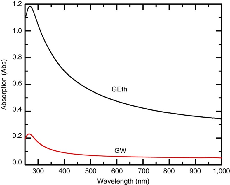
The water-based ink (GW) is prepared by ultrasonicating (Fisherbrand FB15069, Max power 800W) the graphite flakes (Sigma Aldrich Graphite) for 9 h in deionized water with sodium deoxycholate (SDC, 9 mg ml−1)31. The dispersion is then ultracentrifuged (Sorvall WX100 mounting a TH-641 swinging bucket rotor) at 10 k r.p.m. for 1 h to remove thick (>10 nm) flakes. After ultracentrifugation, the top 70% of the dispersion is extracted and used for vacuum filtration and film transfer. We also prepare ethanol-based inks (GEth) by ultrasonicating (1 h) 5 mg ml−1 flakes (Cambridge Nanosystems, GR1) produced by cracking methane and carbon dioxide in a plasma torch. The dispersion is then ultracentrifuged (Beckman Coulter Proteomelab XL-A, with a SW 32 Ti swinging bucket rotor) at 10 k r.p.m. for 1 h and the top 70% is collected for further characterization. Rheological measurements (viscosity, surface tension, density) give ηGW∼1.3 mPa s, γGW∼48 mN m−1, ρGW∼0.8 g cm−3; ηGEth∼2.2 mPa s, γGEth∼30.7 mN m−1, ρGEth∼0.98 g cm−3, consistent with previous reports33,34,35,36,37,38. Optical absorption spectroscopy is used to estimate the flakes concentration18,31,32 via the Beer–Lambert law, which correlates the absorbance A=αcl, with the beam path length l [m], the concentration c [g l−1] and the absorption coefficient α [l g−1 m−1]. Figure 1 plots the absorption spectrum of GW and GEth inks diluted to 1:20 with water and ethanol respectively, to avoid possible scattering losses at higher concentrations. Using α∼1.390 l g−1 m−1 (ref. 31) and α∼2.460 l g−1 m−1 (ref. 18) at 660 nm for GW and GEth, respectively, we obtain cGW∼0.1 mg ml−1 and cGEth∼0.36 mg ml−1.
Figure 1. Absorption spectra.
Absorption of water-based (GW) and ethanol-based (GEth) inks from the visible to near-infrared range.
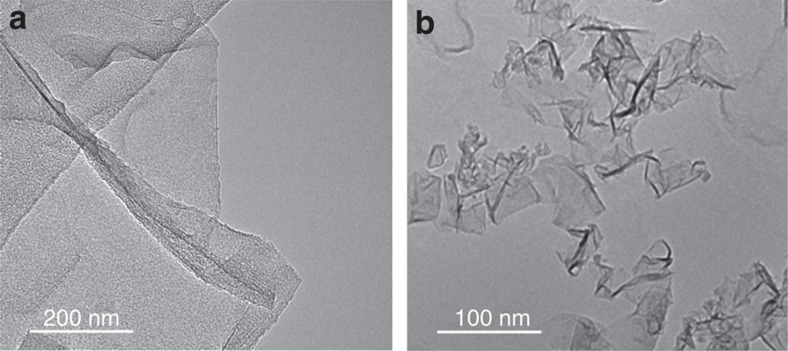
Figures 2a,b show high-resolution transmission electron microscopy (HRTEM) micrographs of a single-layer (SLG) and a few-layer graphene (FLG) flake from the GEth and GW inks, respectively. The associated HRTEM statistics31 from the GW ink shows ∼26% SLG, ∼22% bi- and ∼18% tri-layers with 150-300 nm average size. HRTEM statistics on the GEth flakes show ∼12% SLG, ∼30% bi- and ∼58% multi-layers, with ∼1 μm average size.
Figure 2. Transmission electron microscopy.
Transmission electron microscopy images of (a) single-layer graphene flakes from ethanol based (GEth) and (b) few-layer graphene flakes from water based inks (GW).
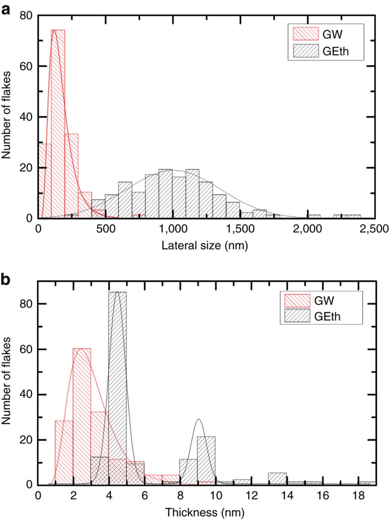
The average lateral size and thickness of the GW and GEth flakes are also estimated by atomic force microscopy (AFM). AFM statistics on the lateral size (Fig. 3a) show a log-normal distribution for the GW flakes peaked at 120 nm with a mean size ∼150 nm and a Gaussian distribution for GEth with a mean size ∼1.04 μm. The mean GW flake thickness is 2.8 nm (peaked at 2.5 nm) indicating that these are FLGs (<5 layers), while ∼57% of the GEth flakes are 4–5 nm thick (Fig. 3b) and ∼20% have higher thickness ∼9 nm.
Figure 3. Flakes distribution.
(a) Flake lateral size distribution and (b) thickness, for water-based (GW) and ethanol-based (GEth) inks.
GSAs are prepared as follows. The first, W-GSA, is made with the GW ink. Approximately 250 μl is vacuum filtered using 100 nm pore-size nitrocellulose filters. This blocks the flakes, while water passes through, leading to a film on the surface of the filter. This is then placed on an intrinsic Si/SiO2 wafer and annealed at ∼80 °C for 2 h, to improve adhesion, followed by dissolution of the filter in acetone overnight. The resulting film is ∼65 nm thick, as determined by AFM. Following the procedure reported in ref. 27, we estimate a density∼0.72 g cm−3 for the W-GSA, derived from the weight (measured with a microbalance) of the filter before and after film deposition. This is ∼1/3 of the density of bulk graphite. Since the graphene flakes27 in W-GSA films are, on average, stacked with the direction parallel to the SiO2 surface, we can assume an interflake distance ∼3 times larger than that of graphite (0.33 nm), which results in ∼1 nm; thus the film thickness corresponds to an equivalent number of layers N∼65.
The second, Eth-GSA, is prepared by inkjet-printing (Fujifilm Dimatix, DMP-2800) the GEth ink on intrinsic Si/SiO2 at an inter-drop spacing of 50 μm for 100 printing passes. The resulting thickness is ∼25 nm. In this case, once the droplets land on the substrate, they spread according to Young’s equation46,47 γSV−γSL−γLVcosθc=0, where γSV [mJ m−2] is the solid–vapour surface energy, γSL is the solid–liquid interfacial tension, and γLV is the liquid–vapour surface tension48. When inkjet printing the GW ink, the high surface tension (γW∼47.8 mN m−1) results in de-wetting (that is, isolated droplets caused by high θc). On the other hand, the lower surface tension of the GEth ink (γGEth∼30.7 mN m−1) offers a lower θc, which causes the droplets to spread and join, enabling morphologically uniform films on Si/SiO2. The boiling point of GEth (∼78 °C) and low surface tension (30.7 mN m−1) minimize the effect of the cohesion forces responsible for the transport of material inside and around a coffee ring49,50.
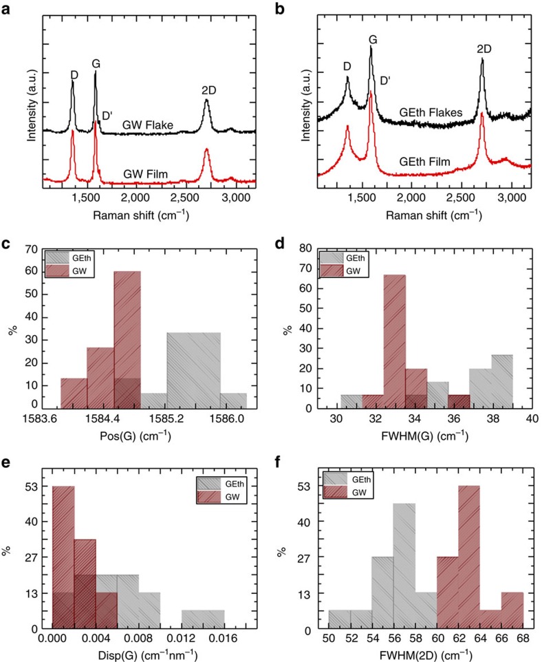
Raman spectroscopy is used to monitor the quality of the flakes at each step of the GSA preparation process for both inks (Fig. 4a,b). Raman spectra are acquired at 457, 514.5 and 633 nm with a Renishaw InVia with a × 50 objective (N.A.=0.85). The power on the sample is kept below 1 mW to avoid possible thermal damage. About 20 measurements are taken in different positions on each sample for each excitation wavelength. The G peak corresponds to the high frequency E2g phonon at Γ, while the D peak, due to the breathing modes of six-atom rings, requires a defect for its activation51,52,53. This arises from the transverse optical phonons around the Brillouin zone edge of the K point51,53, it is activated by a double resonance (DR) process54, and is dispersive with the energy of excitation owing to a Kohn anomaly at the K point55. Double resonance can also occur through an intra-valley process, that is, connecting two points belonging to the same cone around K or K′, which gives rise to the D′ peak. The 2D peak and the 2D′ peak are the second-order resonances of the D and D′ peaks, respectively. 2D and 2D′ are generated from the momentum conservation by two phonons having opposite wave vectors, meaning that for their activation no defects are required, and thus these modes are always active56. The 2D peak is a single Lorentzian in SLG, whereas it splits into several components as the number of layers increases, reflecting the evolution of the electronic band structure56.
Figure 4. Raman spectroscopy.
Raman spectra acquired at 514.5 nm of (a) GW flakes (black) and a GW film deposited on SiO2/Si (red) and of (b) GEth flakes (black) and a GEth film (red). Statistics of (c) Pos(G), (d) FWHM(G), (e) Disp(G) and (f) FWHM(2D) for GEth (grey) and GW (red) films.
In disordered carbon, the position of the G peak, Pos(G) increases when the excitation wavelength λL decreases from the IR to UV52. Furthermore, the dispersion of the G peak, Disp(G)=ΔPos(G)/ΔλL and the full-width-at-half-maximum of the G peak, FWHM(G) both increase with disorder52. The ratio of intensity of the D and G peaks, I(D)/I(G), analysed in combination with FWHM(G) and Disp(G), allows one to discriminate between disorder at the edges of the flakes and in the bulk, where a higher I(D)/I(G) implies a higher FWHM(G) and Disp(G). Figures 4a,b show that the film preparation process does not change the structural properties of the flakes significantly. On the other hand, Figs 4c–f indicate a difference between the GW-based and the GEth-based films, respectively. The GEth shows a more pronounced and wider D peak, as well as a wider G peak. This implies a more defective nature of these flakes. Furthermore, the higher Disp(G) and FWHM(G) indicate that, unlike the GW flakes, the defects are also spread within the flakes themselves. FWHM(2D) in Fig. 4f confirms that the GEth flakes mostly consist of multilayers. The quality of the GW flakes allows us to qualitatively estimate the Fermi energy (EF≤250 meV) and, correspondingly, the doping (≤4 × 1012 cm−2), by combining Pos(G) with the ratio of the 2D and G integrated areas, A(2D)/A(G) (refs 57, 58, 59).
Optical experiments at THz frequencies
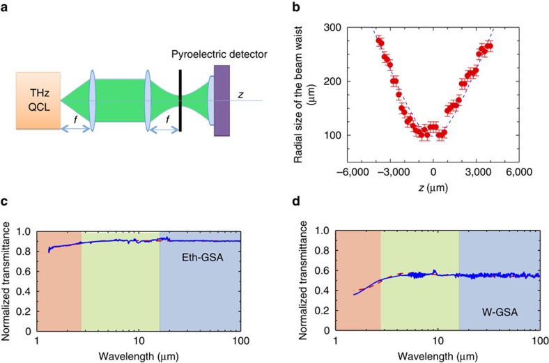
To investigate the THz-induced non-linear absorption properties of GSAs we use the open-aperture z-scan technique30. The 3.5 THz radiation generated by a QCL (single-plasmon waveguide)7 is focused at normal incidence, by using two closely positioned convergent lenses with 3 cm focal length f (Fig. 5a).
Figure 5. Z-scan and FTIR measurements.
(a) Schematic diagram showing the open aperture z-scan setup; (b) beam waist (radial spot size) profile measured at different positions along the optical axis z, of the single-plasmon 3.5 THz QCL operating in pulsed-mode with a pulse width of 2 μs, a modulation frequency of 200 kHz, under an applied field of 7.6 kV cm−1. The error bars represent the uncertainty associated with the measurement of the radius of the beam spot. The fitting function  allows to retrieve a radial spot size w0∼95±6 mm. (c,d) FTIR transmittance of (c) Eth-GSA and (d) W-GSA normalized to the transmittance of the SiO2/Si substrate, in the NIR, MIR and THz spectral ranges. The spectra collected separately in the three spectral ranges are plotted together. A white light source is employed in all cases combined with a PbSe detector (NIR) DTGS KBr detector (MIR) and DTGS-polyethylene detector (THz).
The samples are placed on a purpose-designed holder and translated along the optical axis (z) using a micrometric stage. A pyroelectric detector with a 7 mm2 sensitive area is positioned at a fixed distance from the laser facet, behind the sample holder, to collect the transmitted radiation. The substrate transmittance is also measured and used to normalize the transmittance data. The QCL is operated in pulsed-mode, under different pulsed regimes. For W-GSA, we use a pulse width ∼2 μs and a modulation frequency 100 kHz, corresponding to a 20% duty cycle. For Eth-GSA, we repeat the experiment twice: under identical conditions as for W-GSA (20% duty cycle); and then by reducing the duty cycle, that is, with a pulse width of 1 μs and a modulation frequency 100 kHz, corresponding to 10% duty cycle, to investigate the sample behaviour under shorter pulses. In all cases, a superimposed additional square function modulation at 33 Hz and with 50% duty cycle is added to match the response of the pyroelectric detector.
To determine the QCL beam profile, we perform knife-edge60 measurements at the focal point (red dots in Fig. 5b). We record the total power with the pyroelectric detector as the knife-edge is translated through the beam. From these experiments we extract the beam spot size, which has a characteristic Gaussian shape (fitting function, dashed line in Fig. 5b).
Taking into account the nearly circular Gaussian (x–y) spatial profile and the quasi-continuous wave driving regime of the QCL (so that the beam intensity can be time-independent), the dependence of the absorption coefficient on the pump intensity is expressed as:
 |
where αNS and αS represent the non-saturable and saturable components of the linear absorption α0=α(I=0)=αNS+αS, respectively, I(z) is the beam intensity along the optical axis, and IS is the saturation intensity (that is, the intensity at which the saturable absorption is reduced by 50%). I(z) can be written as a function of the beam intensity at the focal point I0, and of the Rayleigh length, zR, which expresses the distance, along the propagation direction of a beam, from the waist to the place where the area of the cross section is doubled:
 |
From the measurement of the beam profile (Fig. 5b), we extract a radial spot size w0=95±6 μm, corresponding to zR∼330 μm. We also measure at the focal point the average values I0∼1.3 W cm−2 for W-GSA, and I0∼0.7 W cm−2 and ∼1.3 W cm−2 for Eth-GSA, due to the different pulsed operating regimes used for Eth-GSA.
FTIR spectroscopy can be used to determine the linear absorption α0 in the THz, MIR and near-IR (NIR) range61. Spectra are acquired with deuterated triglycine sulfate (DTGS)-polyethylene, DTGS-KBr and PbSe detectors, optimized for THz, MIR and visible frequencies, respectively6.
The FTIR transmission spectra of Eth-GSA and W-GSA in the 3–230 THz range, normalized to the SiO2/Si transmittance, are shown in Fig. 5c,d. These allow us to extract EF, N and to evaluate the carrier scattering dynamics61.
The optical absorption can be written as a function of the sum of the interband conductivity σinter and the intraband conductivity σintra61:
 |
 |
where ω=2πν, ν is the frequency, f is the Fermi distribution, Гib describes the broadening of the interband transitions, and τ is the momentum relaxation time due to carrier intraband scattering. 2Δ represents the material bandgap and is set to zero61.
The optical transmission through N SLG layers on Si/SiO2 normalized to the transmission through the reference Si/SiO2 can be written as61:
 |
where the Si/SiO2 substrate refractive index, nsub, is calculated by using the effective medium theory62 with a volume ratio (SiO2 over Si) of 10−3, and using the values reported in literature for silica glass63 and silicon in the 1–100 μm range.
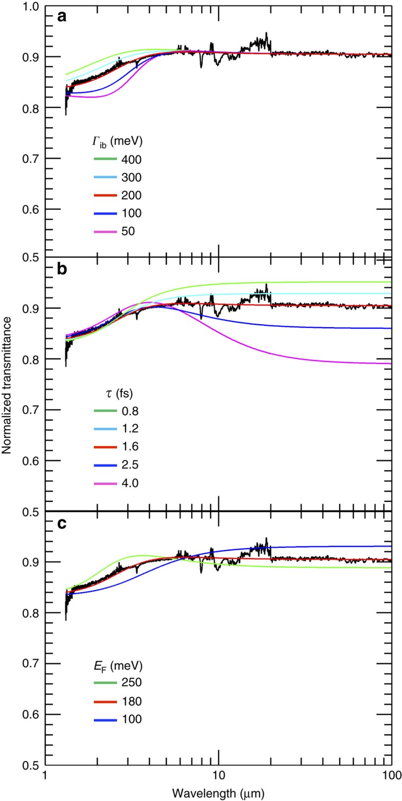
By combining equations (3)–(5), , and assuming that both interband and intraband processes are present, we get the dependence of the optical transmission on N, EF, τ and Гib (ref. 61). Eth-GSA (Fig. 5c) shows an almost flat IR transmittance, which allows us to qualitatively evaluate N∼20 and EF ∼180 meV via a set of iterative fitting procedures (see Methods and Fig. 6a–c).
Figure 6. Analysis of the FTIR spectra of ethanol-based graphene saturable absorber (Eth-GSA).
(a) Dependence on Γib. FTIR transmission spectrum superimposed to fit function (Γib=200 meV, red line) and a set of functions obtained by varying Γib in the range 50–400 meV. (b) Dependence on τ. FTIR transmission spectrum superimposed to fit function (τ=1.64 fs, red line) and a set of functions obtained by varying τ in the range 0.8–4.0 fs. (c) Dependence on EF. FTIR transmission spectrum superimposed to the fit function (EF=181 meV, red line) and a set of functions obtained by varying EF in the range 100–200 meV.
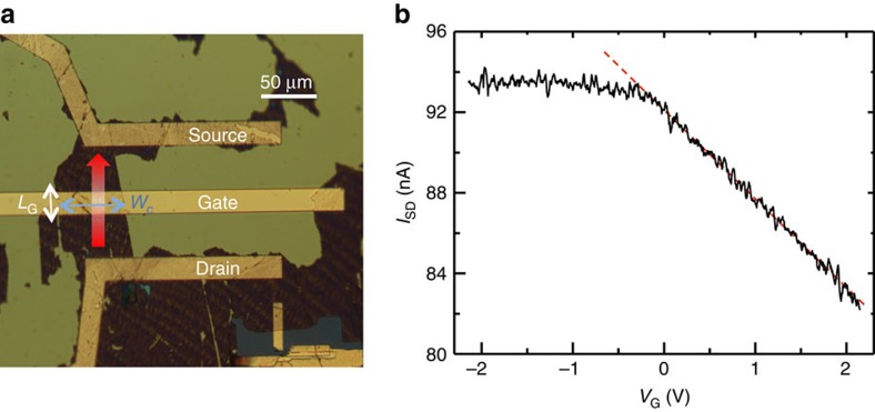
Conversely, the visible absorption cut-off in the transmission spectra of W-GSA (Fig. 5d) allows us to retrieve the above parameters via a more detailed procedure. First we estimate the density of free carriers in W-GSA by fabricating a top-gate FET having as active channel the W-GSA film (Fig. 7a) (see Methods). The source-drain distance is set to 100 μm, and the channel width WC=60 μm, with the top-gate length LG∼20 μm (Fig. 7a). We then perform room-temperature transport measurement and investigate the dependence of the source-to-drain current (ISD) from the bias applied to the gate electrode (VG), while keeping the source-to-drain bias (VSD) equal to 1 mV. The extrapolated sample resistance is ∼11 kΩ at VG=0 V. By increasing VG, ISD decreases linearly, unveiling a characteristic p-type FET behaviour, meaning that the density of majority carriers (holes) decreases (Fig. 7b). From the linear fit to the data (Fig. 7b, dashed line), we extrapolate the transconductance (gm=4.4 nA V−1) and the expected threshold voltage (Vth=20.5 V) for which the linear fit to the data intersects the source-drain current axis. The extrapolated Vth allows us to estimate the density of free carriers (n) at VG=0 V, via the relation64:
Figure 7. Field effect transistor and transport data.
(a) Optical microscope image of a top gate FET with a channel made by printing the water-based ink (W-GSA sample). (b) Dependence of the source-drain FET current (IDS) from the gate bias VG in the range from −2.2 V to +2.2 V, measured while a source-drain voltage VSD=1 mV is applied. The dashed line represents the fit to the data in the linear region and gives a transconductance∼4.4 nA V−1.
 |
where CG=2.1 pF is the gate-to-channel capacitance (see Methods), e is the electric charge and Agated is the gated area, calculated assuming that the full transistor channel is influenced by the gate potential. The extrapolated n approximately corresponds to EF∼250 meV, which is consistent with the EF estimated from Raman spectroscopy56,59. We then fit the transmission data of Fig. 5d by using equations (3)–(5), , and assuming EF=250 meV as initial value for the iterative fitting procedure. The fitting curve, shown as a dashed line in Fig. 5d, gives N∼70 in good agreement with the AFM measurement, EF∼210 meV, Гib∼130 meV and τ∼2 fs.
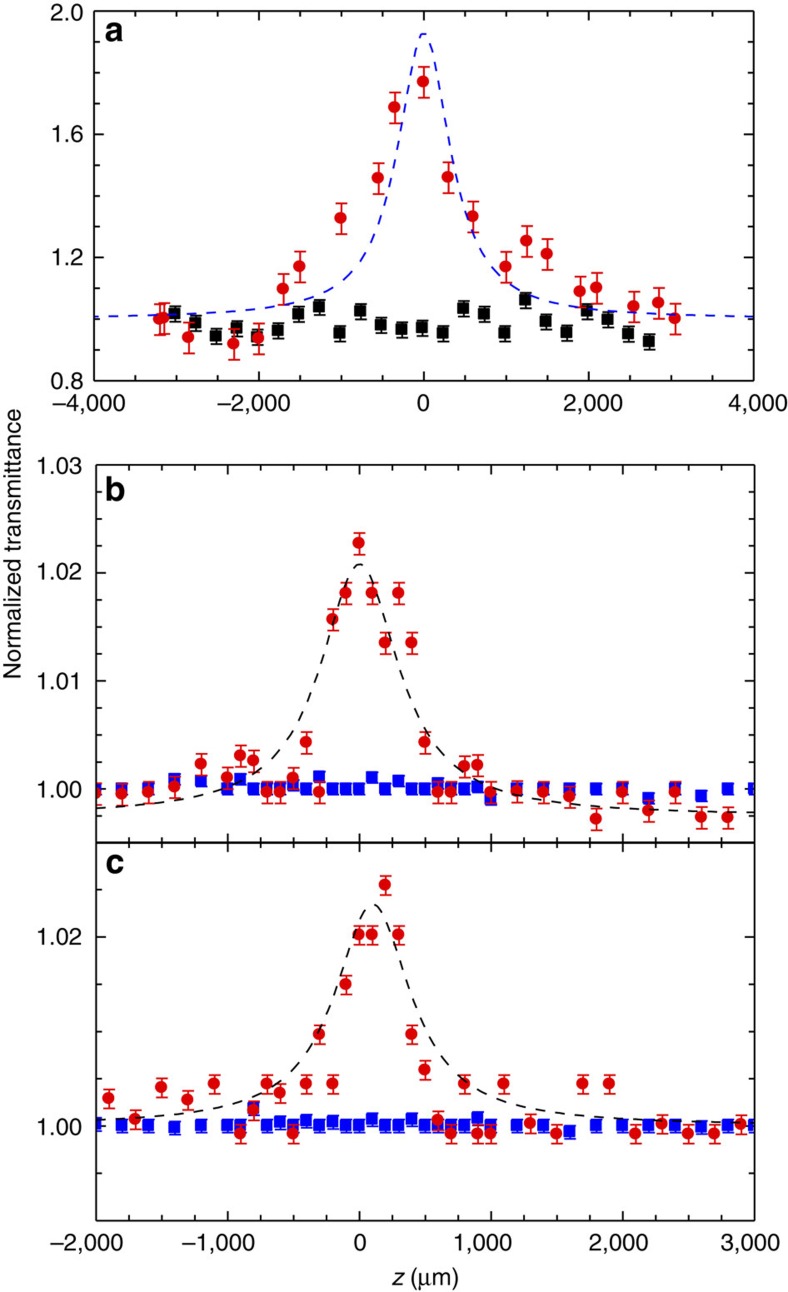
Figure 8a–c plots the z-scan transmission experiments. We detect an increase in transmission in all samples at z=0, where the z-scan trace is maximum, representing a SA signature. The transmission enhancement is significantly larger (80%) in W-GSA, compared with 2.5% in Eth-GSA. The transmission enhancement is constant (within 5%) in all investigated W-GSA and Eth-GSA samples. On the other hand, the Si/SiO2 substrate shows no changes in transmission along the z-axis, confirming that the absorption bleaching is due to the films.
Figure 8. Transparency modulation.
(a–c) z-scan normalized transmittance traces of (a) water-based graphene saturable absorber (W-GSA) (dots) and (b,c) ethanol-based graphene saturable absorber (Eth-GSA) probed with a quantum cascade laser operating at (b) 10% duty cycle, and (c) 20% duty cycle, compared with the z-scan normalized transmittance traces of the Si/SiO2 substrate (squares). The error bars correspond to the uncertainty interval on the measured normalized transmittance. The dashed lines are the fits with equation (7).
The normalized transmittance in the z-scan measurements can be written as65:
 |
By fitting the data in Fig. 8, we extract the saturable and non-saturable absorption coefficients, and the saturation intensity. For W-GSA, αNS∼0.17±0.02, αS∼0.68±0.1 and IS=6.7±1 W cm−2. For Eth-GSA: αNS∼0.08±0.01, αS∼0.17±0.02 when the QCL operates at a 10% duty cycle, and αNS∼0.07±0.01, αS=0.19±0.02 for a 40% duty cycle, showing the negligible role of the device operating conditions. In both cases, the extracted lower saturable absorption values for Eth-GSA reflect the different material quality, in agreement with Raman measurements. The corresponding saturation intensities for Eth-GSA are IS=2.9±0.7 W cm−2 (10% QCL duty cycle) and IS=3.3±0.7 W cm−2 (20% QCL duty cycle). In both W-GSA and Eth-GSA the saturation fluence reaches several μJ cm−2. The maximum αS in W-GSA is 68%, while αNS<17% on average. The αS coefficient is the largest reported to date for any spectral range17,25,28. The saturation intensity values are in agreement with what achieved in the far-IR30 in presence of optical pulses much longer (2 μs) than the demarcation time scale set by the carrier-phonon scattering time (∼150 fs as derived by pump-probe)20,66. Under the above experimental conditions charge carrier distribution develops into quasi-equilibrium within the optical pulse duration.
Typically, non-saturable losses originate from scattering at the interfaces between the layers67, free carrier absorption30 or defects, which depend on the quality of the fabrication techniques. At visible wavelengths, the dominant non-saturable loss is due to scattering losses at the layer interfaces67, unavoidable even in case of defect-free graphene67. Alternative loss dynamics may, however, dominate under specific experimental conditions. For THz excitation, owing to the long wavelength, the multi-interface effect makes only a minor contribution. Additionally, when graphene is doped, non-saturable absorption can be linked to either free carrier absorption or to the reflectivity from the sheets, since in this regime the optical conductivity is well described by the Drude model. Here, at low pumping photon energies (THz frequencies), the optical absorption in graphene is dominated by intraband transitions68. Thus, the dynamics of our THz GSA is governed by ultrafast intraband dynamic.
Discussion
The versatility offered by printable graphene films acting as fast SAs paves the way for new classes of photonic devices in the THz range, with specifically designed device functionalities. The 80% transparency modulation, combined with the flexibility offered by graphene films and inks, can allow, for example, the intra-cavity embedding of SAs in existing THz sources, providing a unique capability for mode-locked and compact THz sources. It will also enable the implementation of ultrafast modulators, filters and mirrors with impacts in the THz frequency range.
Methods
Rheological characterization
The surface tension is measured using the pendent drop method (First Ten Angstroms FTA1000B). The shape of the drop results from the relation between surface tension and gravity. The surface tension is then calculated from the shadow image of a pendant drop using drop shape analysis. The contact angle is measured by dispensing 1 μl of ultrapure DI water on the substrates and measuring the angle at which the ink interface meets the solid surface. A parallel plate rotational rheometer (DHR rheometer TA instruments (GW ink) and Bohlin C-VOR Rheometer (GEth ink)) is used to evaluate the viscosity as a function of shear rate, the infinite-rate viscosity is found for both the GEth and GW inks.
Transmission electron microscopy
Drops of both inks are dispensed on holey carbon TEM grids for HRTEM analysis, using a Tecnai T20 high-resolution electron microscope with an acceleration voltage of 200 kV operating in Bright Field mode.
Atomic force microscopy
A Bruker Dimension Icon working in peakforce mode is used. From the centrifuged dispersion four samples are collected and, after 20 times dilution, they are drop cast onto pre-cleaned (with acetone and isopropanol) Si/SiO2 substrate. Each sample is scanned across three different areas. For each material, 150 flakes are counted.
Vacuum filtration transfer
∼1 ml GW ink is diluted with DI water at a ratio of 1:9 and is passed through a nitrocellulose membrane (100 nm pore size), hastened with the use of a Büchner flask attached to a vacuum pump. The filtered film is then washed with DI water in order to remove residual surfactant. The flakes on the membrane are then rinsed in DI water for 5 min and transferred onto an intrinsic Si/SiO2 substrate. After oven annealing (∼80 °C) the sample is placed in an acetone bath to dissolve the nitrocellulose membrane.
Transistor fabrication
A top-gate FET is fabricated using W-GSA. Source and drain electrodes, shaped as stripes 100 μm distant from each other, are defined via a combination of electron beam lithography and thermal evaporation of a 5/100 nm sequence of Cr/Au. This geometry defines a channel having a100 μm length and an average width of 60 μm, set by the shape of the selected portion of graphene.
A high-k dielectric (HfO2, εr=13–19)69 oxide layer is then placed over the whole transistor plane via atomic layer deposition (ALD). In order to guarantee a good electrical isolation a thickness of 100 nm is chosen for this layer.
The gate electrode is designed as a rectangular stripe having a width WG=20 μm. It is lithographically patterned across the central part of the FET channel with a length (120 μm) suitable to cover the whole channel. The gate to channel capacitance is with a finite element method (COMSOL Multiphysics). We get CG∼2.0–3.0 pF.
Fourier infrared spectroscopy analysis of Eth-GSA samples
Figure 6a plots the FTIR transmission spectrum superimposed to the fit achieved by keeping N, EF and τ as fixed parameters and by varying Γib in the 50–400 meV range. The fitting curve (red curve in Fig. 6a) that well matches the experimental data corresponds to Гib=200 meV and gives: N∼19, EF∼181 meV, corresponding to n∼1.5 × 1012 cm−2, τ∼1.6 fs. Figure 6b interpolates the data by exploiting the same fit function in which N, EF and Гib are fixed parameters. τ is varied in the range 0.8–4.0 fs. The fitting curve (red curve in Fig. 6b) corresponds to τ=1.6 fs and gives: N∼19, EF∼181 meV and Гib∼200 meV. Finally we investigate the influence of EF on the fit. We keep N, τ and Гib as fixed parameters and vary EF in the 100–200 meV range, obtaining: N∼19, Гib∼200 meV and τ∼1.6 fs with EF=180 meV.
Data availability
The data that support the findings of this study are available from the corresponding author on request.
Additional information
How to cite this article: Bianchi, V. et al. Terahertz saturable absorbers from liquid phase exfoliation of graphite. Nat. Commun. 8, 15763 doi: 10.1038/ncomms15763 (2017).
Publisher’s note: Springer Nature remains neutral with regard to jurisdictional claims in published maps and institutional affiliations.
Supplementary Material
Acknowledgments
We acknowledge funding from ERC grants SPRINT, Hetero2D, HiGRAPHINK, the EU Graphene Flagship, and EPSRC grants EP/K01711X/1, EP/K017144/1, EP/L016087/1 and EP/N010345/1.
Footnotes
The authors declare no competing financial interests.
Author contributions M.S.V. conceived the experiments. V.B. and L.V. performed the optical experiments; T.C. and F.T. prepared the graphene inks, performed TEM characterization and printed the graphene saturable absorbers. T.C. performed UV–vis, Rheometry and AFM characterization. T.C., L.V., D.Y., P.G.K., L.Lo., F.T., A.C.F. performed and analysed the micro-Raman experiments; V.B., L.V. and M.S.V. modelled and analysed the data. V.B., L.V., T.C., A.T., A.C.F., F.T., M.S.V. discussed the results. L. Li., E.H.L. and A.G.D. grew the QCL material. M.S.V. fabricated and characterized the QCL. L.V. fabricated and characterized the FET device. M.S.V., F.T. and A.C.F. wrote the manuscript with contributions and discussions from all authors.
References
- Tong S. et al. Phase noise investigation of multicarrier sub-THz wireless transmission system based on an injection-locked gain-switched laser. IEEE Trans. Terahertz Sci. Technol. 5, 590–597 (2015). [Google Scholar]
- Korobenko A., Milner A. A. & Milner V. Direct observation, study, and control of molecular superrotors. Phys. Rev. Lett. 112, 113004 (2014). [DOI] [PubMed] [Google Scholar]
- Eisele M. et al. Ultrafast multi-THz nano-spectroscopy with sub-cycle temporal resolution. Nat. Photon. 8, 841–845 (2014). [Google Scholar]
- Kampfrath T., Tanaka K. & Nelson K. A. Resonant and non-resonant control over matter and light by intense terahertz transients. Nat. Photon. 7, 680–690 (2013). [Google Scholar]
- Tonouchi M. Cutting edge terahertz technologies. Nat. Photon. 1, 97–105 (2007). [Google Scholar]
- Vitiello M. S., Scalari G., Williams B. & De Natale P. Quantum Cascade Lasers: 20 years of challenges. Opt. Express 23, 5167–5182 (2015). [DOI] [PubMed] [Google Scholar]
- Li L. et al. Terahertz quantum cascade lasers with >1 W output powers. Electron. Lett. 50, 309–311 (2014). [Google Scholar]
- Vitiello M. S. et al. Quantum-limited frequency fluctuations in a Terahertz laser. Nat. Photon. 6, 525–528 (2012). [Google Scholar]
- Keller U. Recent developments in compact ultrafast lasers. Nature 424, 831–838 (2013). [DOI] [PubMed] [Google Scholar]
- Keller U. et al. Semiconductor saturable absorber mirrors (SESAMs) for femtosecond to nanosecond pulse generation in solid-state lasers. IEEE J. Sel. Top. Quantum Electron. 2, 435–453 (1996). [Google Scholar]
- Lagatsky A. A. et al. Low-loss quantum-dot-based saturable absorber for efficient femtosecond pulse generation. Appl. Phys. Lett. 91, 231111 (2007). [Google Scholar]
- Hoffmann M. C. & Turchinovich D. Semiconductor saturable absorbers for ultrafast terahertz signals. Appl. Phys. Lett. 96, 151110 (2010). [Google Scholar]
- Köhler R. et al. Terahertz semiconductor-heterostructure laser. Nature 417, 156–159 (2002). [DOI] [PubMed] [Google Scholar]
- Wang F. et al. Generating ultrafast pulses of light from quantum cascade lasers. Optica 2, 944–949 (2015). [Google Scholar]
- Maysonnave J. et al. Mode-locking of a terahertz laser by direct phase synchronization. Opt. Express 20, 20855–20862 (2012). [DOI] [PubMed] [Google Scholar]
- Barbieri S. et al. Coherent sampling of active mode-locked terahertz quantum cascade lasers and frequency synthesis. Nat. Photon. 5, 306–313 (2011). [Google Scholar]
- Sun Z. et al. Graphene mode-locked ultrafast laser. ACS Nano 4, 803–810 (2010). [DOI] [PubMed] [Google Scholar]
- Hasan T. et al. Solution-phase exfoliation of graphite for ultrafast photonics. Phys Status Solidi Basic Res. 247, 2953–2957 (2010). [Google Scholar]
- Wang F. et al. Wideband-tuneable, nanotube mode-locked, fibre laser. Nat. Nanotechnol. 3, 738–742 (2008). [DOI] [PubMed] [Google Scholar]
- Brida D. et al. Ultrafast collinear scattering and carrier multiplication in graphene. Nat. Commun. 4, 1987 (2013). [DOI] [PubMed] [Google Scholar]
- Bonaccorso F. et al. Mater. Today 15, 564–589 (2012). [Google Scholar]
- Ferrari A. C. et al. Science and technology roadmap for graphene, related two-dimensional crystals, and hybrid systems. Nanoscale 7, 4598–4810 (2015). [DOI] [PubMed] [Google Scholar]
- Tredicucci A. & Vitiello M. S. Device Concepts for Graphene-Based Terahertz Photonics. IEEE J. Sel. Top. Quantum Electron. 20, 8500109 (2014). [Google Scholar]
- Sun Z. et al. A stable, wideband tunable, near transform-limited, graphene-mode-locked, ultrafast laser. Nano Res. 3, 653–660 (2010). [DOI] [PubMed] [Google Scholar]
- Baek I. H. et al. Efficient mode-locking of Sub-70-fs Ti:sapphire laser by graphene saturable absorber. Appl. Phys. Express 5, 032701 (2012). [Google Scholar]
- Zaugg C. A. et al. Ultrafast and widely tuneable vertical-external-cavity surface-emitting laser, mode-locked by a graphene-integrated distributed Bragg reflector. Opt. Express 21, 31548–31559 (2013). [DOI] [PubMed] [Google Scholar]
- Mary R. et al. 1.5 GHz picosecond pulse generation from a monolithic waveguide laser with a graphene-film saturable output coupler. Opt. Express 21, 7943–7950 (2013). [DOI] [PubMed] [Google Scholar]
- Zhang M. et al. Tm-doped fiber laser mode-locked by graphene-polymer composite. Opt. Express 20, 25077–25084 (2012). [DOI] [PubMed] [Google Scholar]
- Cizmeciyan M. N. et al. Graphene mode-locked femtosecond Cr:ZnSe laser at 2,500 nm. Opt. Lett. 38, 341–343 (2013). [DOI] [PubMed] [Google Scholar]
- Bianco F. et al. THz saturable absorption in turbostratic multilayer graphene on silicon carbide. Opt. Express 23, 11632–11640 (2015). [DOI] [PubMed] [Google Scholar]
- Lotya M. et al. Liquid phase production of graphene by exfoliation of graphite in surfactant/water solutions. J. Am. Chem. Soc. 131, 3611–3620 (2009). [DOI] [PubMed] [Google Scholar]
- Hernandez Y. et al. High-yield production of graphene by liquid-phase exfoliation of graphite. Nat. Nanotechnol. 3, 563–568 (2008). [DOI] [PubMed] [Google Scholar]
- Torrisi F. et al. Stable, surfactant-free graphene-styrene methylmethacrylate composite for ultrafast lasers. Adv Opt. Mater. 4, 1088–1097 (2016). [Google Scholar]
- Torrisi F. et al. Inkjet-printed graphene electronics. ACS Nano 6, 2992–3006 (2012). [DOI] [PubMed] [Google Scholar]
- Torrisi F. & Coleman J. N. Electrifying inks with 2D materials. Nat. Nanotechnol. 9, 738–739 (2014). [DOI] [PubMed] [Google Scholar]
- Krebs F. C. Fabrication and processing of polymer solar cells: A review of printing and coating techniques. Sol Energy Mater Sol Cells 93, 394 (2009). [Google Scholar]
- Secor E. B., Prabhumirashi P. L., Puntambekar K., Geier M. L. & Hersam M. C. Inkjet printing of high conductivity, flexible graphene patterns. J. Phys. Chem. Lett. 4, 1347–1351 (2013). [DOI] [PubMed] [Google Scholar]
- Ciesielski A. & Samorì P. Graphene via sonication assisted liquid-phase exfoliation. Chem. Soc. Rev. 43, 381–398 (2014). [DOI] [PubMed] [Google Scholar]
- Oka A. & Tominaga K. Terahertz spectroscopy of polar solute molecules in non-polar solvents. J. Non-Cryst. Solids 352, 4606–4609 (2006). [Google Scholar]
- D’Angelo F., Mics Z., Bonn M. & Turchinovich D. Ultra-broadband THz time-domain spectroscopy of common polymers using THz air photonics. Opt. Express 22, 12475–12485 (2014). [DOI] [PubMed] [Google Scholar]
- Derby B. & Reis N. Inkjet printing of highly loaded particulate suspensions. MRS Bull. 28, 815–818 (2003). [Google Scholar]
- Fromm J. E. Numerical calculation of the fluid dynamics of drop-on-demand jets. IBM J. Res. Dev. 28, 322–333 (1984). [Google Scholar]
- Zhou K. G., Mao N. N., Wang H. X., Peng Y. & Zhang H. L. A mixed-solvent strategy for efficient exfoliation of inorganic graphene analogues. Angew. Chemie Int. Ed. 50, 10839–10842 (2011). [DOI] [PubMed] [Google Scholar]
- Halim U. et al. A rational design of cosolvent exfoliation of layered materials by directly probing liquid–solid interaction. Nat. Commun. 4, 2213 (2013). [DOI] [PMC free article] [PubMed] [Google Scholar]
- Khattab I. S., Bandarkar F., Fakhree M. A. A. & Jouyban A. Density, viscosity, and surface tension of water+ethanol mixtures from 293 to 323 K. Korean J. Chem. Eng. 29, 812–817 (2012). [Google Scholar]
- Israelachvili J. in Intramolecular and Surface Forces Academic Press (1991). [Google Scholar]
- Young T. An essay on the cohesion of fluids. Philos. Trans. R. Soc. Lond. 95, 65 (1805). [Google Scholar]
- Babinec S. J. & Cornell M. C. in Coatings of Polymers and Plastics (eds Ryntz, R. A., Yaneff, P. V.) 1–47 (Marcel Dekker, Inc., 2003).
- Deegan R. D. et al. Capillary flow as the cause of ring stains from dried liquid drops. Nature 389, 827–829 (1997). [Google Scholar]
- Shih C.-J. et al. Bi- and trilayer graphene solutions. Nat. Nanotechnol. 6, 439–445 (2011). [DOI] [PubMed] [Google Scholar]
- Tuinstra F. & Koenig J. L. Raman spectrum of graphite. J. Chem. Phys. 53, 1126–1130 (1970). [Google Scholar]
- Ferrari A. C. & Robertson J. Resonant Raman spectroscopy of disordered, amorphous, and diamondlike carbon. Phys. Rev. B 64, 075414 (2001). [Google Scholar]
- Ferrari A. C. & Robertson J. Interpretation of Raman spectra of disordered and amorphous carbon. J. Phys. Rev. B 61, 14095–14107 (2000). [Google Scholar]
- Thomsen C. & Reich S. Double resonant Raman scattering in graphite. Phys. Rev. Lett. 85, 5214–5217 (2000). [DOI] [PubMed] [Google Scholar]
- Piscanec S., Lazzeri M., Mauri F., Ferrari A. C. & Robertson J. Kohn anomalies and electron–phonon interactions in graphite. Phys. Rev. Lett. 93, 185503 (2004). [DOI] [PubMed] [Google Scholar]
- Ferrari A. C. et al. Raman spectrum of graphene and graphene layers. Phys. Rev. Lett. 97, 187401 (2006). [DOI] [PubMed] [Google Scholar]
- Basko D. M., Piscanec S. & Ferrari A. C. Electron–electron interactions and doping dependence of the two-phonon Raman intensity in graphene. Phys. Rev. B 80, 165413 (2009). [Google Scholar]
- Das A. et al. Monitoring dopants by Raman scattering in an electrochemically top-gated graphene transistor. Nat. Nanotechnol. 3, 210–215 (2008). [DOI] [PubMed] [Google Scholar]
- Bruna M. et al. Doping dependence of the Raman spectrum of defected graphene. ACS Nano 8, 7432–7441 (2014). [DOI] [PubMed] [Google Scholar]
- De Araújo M. A., Silva R., de Lima E., Pereira D. P. & de Oliveira P. C. Measurement of Gaussian laser beam radius using the knife-edge technique: improvement on data analysis. Appl. Opt. 48, 393–396 (2009). [DOI] [PubMed] [Google Scholar]
- Dawlaty J. M. et al. Measurement of the optical absorption spectra of epitaxial graphene from terahertz to visible. Appl. Phys. Lett. 93, 131905 (2008). [Google Scholar]
- Levy O. & Stroud D. Maxwell Garnett theory for mixtures of anisotropic inclusions: application to conducting polymers. Phys. Rev. B 56, 8035 (1997). [Google Scholar]
- Kitamura R., Pilon L. & Jonasz M. Optical constants of silica glass from extreme ultraviolet to far infrared at near room temperature. Appl. Opt. 46, 8118–8133 (2007). [DOI] [PubMed] [Google Scholar]
- Li L. et al. Black phosphorus field-effect transistors. Nat. Nanotechnol. 9, 372–377 (2014). [DOI] [PubMed] [Google Scholar]
- Zheng Z. et al. Microwave and optical saturable absorption in graphene. Opt. Express 20, 23201–23214 (2012). [DOI] [PubMed] [Google Scholar]
- George P. A. et al. Ultrafast optical-pump terahertz-probe spectroscopy of the carrier relaxation and recombination dynamics in epitaxial graphene. Nano Lett. 8, 4248–4251 (2008). [DOI] [PubMed] [Google Scholar]
- Bao W. S., Liu S. Y. & Lei X. L. Hot-electron transport in graphene driven by intense terahertz fields. Phys. Lett. A 374, 1266–1269 (2010). [Google Scholar]
- Mak K. F., Ju L., Wang F. & Heinz T. F. Optical spectroscopy of graphene: from the far infrared to the ultraviolet. Solid State Commun. 152, 1341–1349 (2012). [Google Scholar]
- Vicarelli L. et al. Graphene field-effect transistors as room-temperature terahertz detectors. Nat. Mater. 11, 865–871 (2012). [DOI] [PubMed] [Google Scholar]
Associated Data
This section collects any data citations, data availability statements, or supplementary materials included in this article.
Supplementary Materials
Data Availability Statement
The data that support the findings of this study are available from the corresponding author on request.


