Abstract
Growth of high quality and monolayer graphene on copper thin films on silicon wafers is a promising approach to massive and direct graphene device fabrication in spite of the presence of potential dewetting issues in the copper film during graphene growth. Current work demonstrates roles of a nickel adhesion coupled with the copper film resulting in mitigation of dewetting problem as well as uniform monolayer graphene growth over 97 % coverage on films. The feasibility of monolayer graphene growth on Cu-Ni alloy films as thin as 150 nm in total is also demonstrated. During the graphene growth on Cu-Ni films, the nickel adhesion layer uniformly diffuses into the copper thin film resulting in a Cu-Ni alloy, helping to promote graphene nucleation and large area surface coverage. Furthermore, it was found that the use of extremely thin metal catalyst films also constraint the total amount of carbon that can be absorbed into the film during growth, which helps to eliminate adlayer formation and promote monolayer growth regardless of alloying content, thus improving the monolayer fraction of graphene coverage on the thinner films. These results suggest a path forward for the large scale integration of high quality, monolayer graphene into nanoelectronic and nanomechanical devices.
1 Introduction
Graphene has been paid attention to for the last ten years due to its outstanding material properties [1–3]. However, reliable and large-scale fabrication of high quality and monolayer graphene on metal catalysts remains a problem that limits its use in electronic and mechanical devices. A variety of methods have been used to produce graphene including mechanical exfoliation of graphene from graphite [4], high-temperature decomposition of SiC [5], and chemical vapor deposition (CVD) of polycrystalline graphene on thin nickel films [6], or copper foils [7]. State-of-art high-quality single crystals of graphene has been achieved by controlling the oxidation of copper foils using CVD [8,9]. The problems with applications of graphene often arise during the manual transfer of graphene to the device substrate. Various studies on the transfer of graphene transfer using solution based transfer as well as mechanical transfer [10,11] have been conducted and it has been shown that the transfer process significantly deteriorates electrical properties of graphene [12]. CVD of graphene on copper thin films has shown great promise for large-scale production of graphene for application in nano, micro-electromechanical systems since it can maintain high quality material over large areas [13,14] and can be integrated into conventional micro- and nanofabrication processes [15] without transferring the graphene onto substrates. Therefore, graphene growth on thin films has the potential to enable large area production of graphene with low manufacturing costs.
Unfortunately, CVD growth of graphene on copper films requires to be done on relatively thick films (≈ 1 μm thick) due to stability and dewetting issues of copper thin films at the required process temperature (≈ 1000 °C) [16]. As-deposited metal thin films are metastable and 30% of thin film is known to evaporate during the growth. Therefore, these films tend to dewet from silicon or SiO2 surfaces and form voids in the metal film. If this process continues for a period of time, the metal films will agglomerate into discrete metal islands. This phenomenon creates a major limitation for the growth of graphene on copper thin films since the morphology of the copper surfaces is directly related to formation of graphene nucleation seeds [17].
Overall, this dewetting process typically limits the growth of graphene on thin copper film that are at least 1 μm thick. This is unfortunate since the ability to grow graphene on extremely thin films could offer several advantages. First, the deposition of thin copper films compared to thick films can reduce costs and overall time for processing. Second, graphene films are generally separated from the copper surface by etching away the copper. Therefore, thin copper films lead to decreased copper waste and fabrication costs. Finally, thin metal films are more compatible with standard MEMS and microelectronics fabrication methods compared to thick films. For example, the nanoelectromechanical (NEMS) application of graphene has been limited due to difficulties in integrating the fabrication process of the NEMS structures with graphene growth [15,18]. Having a metal layer thicker than 500 nm is an obstacle to NEMS device fabrication processes due to the fact that any patterned electrodes below the copper layer will be too far away from the graphene to actuate or sense the motion of the graphene NEMS structure accurately [19]. Therefore, it is critical for the advancement of graphene device manufacturing to enable the growth of graphene on nanoscale thin (< 500 nm) copper films.
Graphene growth on copper thin films with thicknesses greater than 500 nm can exhibit extremely high quality and can be used to grow graphene at the wafer scale. For example, monolayer graphene growth on annealed Cu (111) films with extremely high quality (comparable to that of exfoliated monolayer graphene) has been demonstrated by Tao et al[13]. Barrier layers are sometimes used to enhance the adhesion of the copper to the Si/SiO2 surface and promote growth on copper films down to ≈ 500 nm thicknesses [16]. However, below 500 nm, the copper film starts to become unstable and dewet. For example, graphene growth on a 450 nm thick copper thin film done by Ismach et al [20] exhibited surface with graphene residing on top of the dewet copper structures. These films are an example of extreme evaporation and vacancies formation in the copper thin film. Sun et al. [21] reported graphene growth on 300 nm thick copper thin films using a process with low partial pressure of methane gas. The results of this growth showed continuous graphene with electrical properties comparable to that of graphene grown on copper foils but with a small D peak in the Raman spectra which indicates the presence of defects in the carbon lattice of the graphene. Lee et al. [22] also reported graphene growth on 206 nm copper thin films using a low-pressure, fast-heating chemical vapor deposition growth method. However, these growths resulted in highly defective graphene structures as indicated by the large D peak shown by Raman spectroscopy. These defects are likely due to the coarsening of the thin film during the growth process and the difficulty of nucleating graphene grains on extremely thin films. Therefore, growth on sub-500 nm copper films is a major challenge for graphene devices. In this paper, we report on the use of a Cu-Ni alloy to help reduce film coarsening and promote graphene nucleation on thin film thickness below 500 nm.
2 Background
2.1 Dewetting in Copper thin film
Scanning electron microscopy (SEM) in Fig. 1 shows the formation of voids in the copper film when thin films with sub-500 nm thickness were used. These voids are due to capillary forces which act to reduce the free energy of the film interface. This agglomeration process is driven by the high interfacial energy between the metal and the Si/SiO2 substrate surface. When thermal energy is introduced into the system, the metal atoms in the thin film rearrange in order to minimize the total energy of metal and substrate as well as the interfacial energy between the metal and the Si/SiO2 [23]. The metal thin films rearrange themselves to minimize the area in contact with the substrate due to the fact that the interfacial energy between the metal layer and the substrate is typically much larger than the metal the substrate surface energies. This results in the formation of voids in the thin film, followed by the complete dewetting of the metal film into discrete islands. It should be noted that dewetting can occur at temperatures below the melting point of the metal due to the surface diffusion phenomenon during processes. Thus, the dewetting can be accelerated by decreasing film thickness due to the fact that a higher percentage of the total system energy is in the interface as the film thickness decreases [16].
Figure 1.

SEM images of as-grown graphene on copper thin film. (a) 1000 nm thick Cu showing absence of dewettting (b) dewettings on 500 nm thick Cu.
A void will form if the nucleation conditions in Equation 1 are met where R is the average radius of grain sizes, t is the film thickness and θ is the wetting angle of the metal to the substrate as given by Young's equation [24].
| Equation 1 |
This equation indicates that the formation of holes in the copper thin film can be suppressed by increasing the copper film thickness and decreasing the wetting angle,. Therefore, reducing the wetting angle between the copper and the SiO2 substrate could allow for atmospheric-pressure CVD growth of graphene on much thinner films (t < 300 nm).
2.2 Use of Adhesion Layers in Graphene Growth
Several types of adhesion layers have been used to minimize the dewetting of copper films at high temperatures. For example, Levendorf et al. [16] used a 5 nm thick nickel layer as an adhesion promoter. This adhesion layer did not significantly affect the quality of the graphene grown but did help to promote adhesion of the copper to the substrate. Using only nickel as a thin film structure, however, promotes multilayer graphene growth hence it is very difficult to obtain monolayer graphene coverage of greater than 80% on pure nickel films [25]. Other barrier layers such as tungsten, chromium, silicon nitride, aluminum oxide, and sapphire have been investigated to determine their effect on graphene growth, copper film dewetting, and graphene quality with mixed results [26]. In this study, we chose a 50 nm thick layer of nickel as the adhesion layer of interest because of its (1) low interfacial energy with Si/SiO2 surfaces (nickel as thin as 100 nm can survive at temperatures up to 1000 °C without dewetting [25]), (2) ability to form uniform solutions with copper [27], and (3) ability to nucleate high quality graphene films in the CVD process [28,29].
3 Experimental Methods
3.1 Metal Deposition
The Cu-Ni thin films presented in this paper were prepared by electron beam evaporation of the metals onto silicon wafers with 285 nm thermal oxide. First, a 50-nm nickel adhesion layer was deposited onto the silicon wafer. Then the copper was deposited onto each substrate without breaking vacuum. The thicknesses of the deposited copper layers were: 50 nm, 100 nm, 150 nm, 200 nm, 250 nm, 500 nm, 750 nm, and 1000 nm confirmed by profilometer.
3.2 Graphene Growth
The CVD graphene was grown in a standard furnace under atmospheric pressure. The growth furnace uses a conventional Atmospheric Pressure Chemical Vapor Deposition (APCVD)1 system which consists of gas cylinders, flow controllers, an one-inch diameter quartz tube, a heating element, and a vacuum pump in Fig. 2(a). Argon, hydrogen, and methane gas sources are controlled via flow controllers.
Figure 2. (a) Overview of APCVD system (b) Schematic of the region where graphene is synthesized on Si substrate.

Prior to the graphene growth, the tube is pumped down to the range of 0.25 Pa to 0.50 Pa (2 mTorr to 4 mTorr) to remove oxygen from the growth chamber. 8.33 cm3/s (500 sccm) of argon is then introduced into the chamber as the carrier gas with 3.33 cm3/s (200 sccm) of hydrogen as the reducing gas. At this time, pressure inside the tube is constantly kept in the range of 133.3 Pa to 6.7 kPa (1 Torr to 50 Torr). The hydrogen helps to reduce the oxygen concentration level, to etch excessive and weakly bound carbon layers on the copper substrate during graphene growth, and to lower the surface roughness [30]. Next, the tube is slowly heated at a rate of approximately 25 °C per minute with the growth substrate in the furnace. When the temperature of the furnace reaches 1000 °C, 0.083 cm3/s (5 sccm) of methane gas is introduced into the tube in order to initiate the graphene growth. It should be noted that growth step in the current work, specifically, does not include an annealing step to minimize the dewetting issues. Growth is allowed to continue for 5 min before the sample is removed from the heat zone of the furnace. Substrate is then allowed to rapidly cool inside the furnace before the gas is turned off [30]. After approximately 30 minutes of cooling the gas is turned off and the sample is removed from the furnace. Graphene growth recipe, and the overall temperature profile versus time are shown in Fig. 3(a) and (b).
Figure 3. (a) Graphene growth recipe (b) Graphene growth temperature profile versus time.

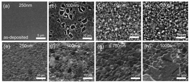
During the graphene growth process, copper was recrystallized as we expected as shown in Fig. 4(b)-(h) compared to as-deposited state Fig. 4(a). The ultimate copper grain size is dependent on the initial film thickness, growth time and growth temperature. From these images, it can clearly be seen that grain size of copper thin film increases as the thickness of copper thin film increases [31].
Figure 4. SEM images of copper grains (a) before the growth of 250 nm, after growth of (b)-(h) Cu film thicknesses with same 50 nm Ni film thickness.
3.3 Graphene Transfer
After the graphene is grown on the Cu-Ni thin films, it is transferred to Si/SiO2 substrates for further examination. Once graphene was synthesized on Cu-Ni alloy thin film, it was spin-coated with polymethyl methacrylate (PMMA). The copper is then etched away in ammonium persulfate (APS) solution of 0.5 mol/L with an etch rate around 0.7 nm/min. According to various etching tests, it was found that slow etching rate of copper thin film reduces defects and wrinkles of the transferred graphene on silicon oxide. In addition, the slower etch rates generally resulted in better yield of the transferred PMMA/graphene samples. The PMMA/graphene film was carefully transferred to a de-ionized water bath to get rid of any copper etchant on PMMA/graphene film. The film was scooped up by a piece of Si/SiO2 strip while the graphene side faced the surface of Si/SiO2. In order to get rid of trapped water between graphene and Si/SiO2, a whole sample was stored in the vacuum chamber, which pumped out trapped water for a day. Formations of wrinkles as well as crack on the graphene are common issues during removal of PMMA backing layer. Thus, samples were baked to 300 °C resulting in the PMMA layer to be relaxed and conform to Si/SiO2 surface. After baking, the PMMA layer was completely removed in acetone bath.
4 Results and Discussion
4.1 Graphene Growth on Cu-Ni Alloys
In order to examine the effect of copper thickness deposited on nickel adhesion layer, graphene was grown on selected copper film by various thickness — 100 nm, 150 nm, 200 nm, 250 nm, 500 nm, 750 nm, and 1000 nm — each on 50-nm thick nickel adhesion layer. Raman spectroscopy (Witec Micro-Raman Spectrometer Alpha 300, λ = 488 nm) was used to estimate the coverage of graphene as well as the number of graphene layers for each sample (Fig. 5). Inset Raman spectrum and color represents a data harvested from a pixel with a same color. I2D/G Raman maps of 30 × 30 μm2 scale reveals the ratio of the intensities of the 2D to G peaks of the graphene grown on each Cu-Ni alloy thicknesses.
Figure 5.
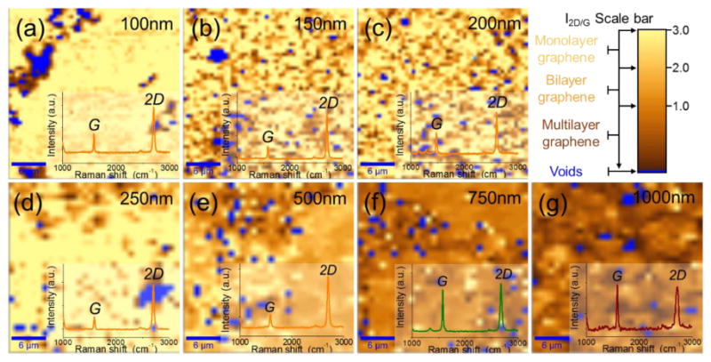
30×30 μm2 scale I2D/G intensity Raman map of graphene grown on Cu-Ni alloy with each corresponding copper film thicknesses. Brighter yellow color map represents higher 2D/G ratio which is closer to monolayer graphene. Each spectra line color presents data harvested from the same colored region, (a) 100 nm, (b) 150 nm, (c) 200 nm, (d) 250 nm, (e) 500 nm, (f) 750 nm, (g) 1000 nm
Overall, these results show that high quality, monolayer graphene with large coverage areas can be formed on copper film thicknesses down to 250 nm using a 50 nm nickel adhesion layer. In fact, most of films show good graphene coverage (> 90%) and very low defect intensities (D peak). In order to further analyze graphene coverage associated with the thickness of the metal catalyst, as-grown graphene on the metal catalyst was characterized by SEM (Quanta FEG 600) as well as Raman, respectively.
Raman spectroscopy and SEM images were analyzed using image processing software (imageJ [32]) to determine the local graphene coverage (Raman measurements), and global coverage (SEM images). Image processing software used color contrast to calculate the coverage percentage of monolayer and bilayer graphene from I2D/G Raman map. The results of this analysis is presented in Table 1.
Table 1. Average global surface roughness of Cu film across 120×160 μm2 surfaces, coverage of transferred graphene measured by SEM image and image processing software, and monolayer-bilayer coverage processed by analyzing three sets of Raman map data from each Cu-Ni thicknesses.
| Cu thickness in Cu-Ni (nm) | Global1 roughness (nm) | Coverage2 (transferred, %) | Monolayer3 coverage (% of Coverage) | >Bilayer3 coverage (% of Coverage) |
|---|---|---|---|---|
| 100 | 96 | 46 | 95 | 5 |
| 150 | 50 | 78 | 99 | 1 |
| 200 | 55 | 88 | 96 | 4 |
| 250 | 53 | 97 | 97 | 3 |
| 500 | 69 | 94 | 80 | 20 |
| 750 | 54 | 98 | 74 | 26 |
| 1000 | 58 | 97 | 56 | 44 |
Optical profilometer
Measurement by SEM
Measurement by Raman
The results of monolayer and multilayer coverage grown on Cu-Ni alloy according to copper thicknesses are shown in Fig. 6 where error bars represent one standard deviation according to Raman spectroscopy data at three different locations of each sample. These results show the functional relation such that the coverage of graphene as well as the portion of bilayer graphene increase as the thickness of thin copper catalyst increase. Interestingly, these results show opposite tendencies from previously reported research on Cu-Ni alloy foils where multilayer graphene is favored to grow on Cu-Ni alloys with higher nickel concentrations [33]. The thinner copper thin film samples used in the current work have higher nickel concentrations compared to the thicker copper thin film since the nickel thin film thickness is kept at 50 nm throughout the samples. However, coverage of monolayer graphene is higher on thinner copper thin film samples. It is likely that the thin films samples have crossed a thickness threshold where nickel concentration has less of an impact on number of graphene layer growth, rather limitation of carbon absorption in small volume of extremely thin Cu-Ni alloy film played a dominant role on graphene growth. Hence, increased overall volume of Cu-Ni alloy in thicker films provides sufficient carbon atoms to segregate to surface during cooling, forming additional graphene layers. Graphene growth using increased methane ratio, increased hydrogen ratio, cooling effect, and different growth time demonstrates this trends in detail. Additional information can be found in Supplementary Information.
Figure 6.
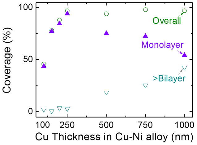
A graph of coverage of transferred graphene measured by Raman spectroscopy with proportion of monolayer and multilayer graphene. Coverage proportion of multilayer graphene increases as Cu thickness increases. Error bars represent coverage variations according to Raman spectroscopy data obtained from three different locations from each sample.
4.2 Coarsening of Cu-Ni Grain Structure during Growth
In order to understand relation between the morphology and structure of the metal films affected during growth, the roughness of Cu-Ni films was measured using atomic force microscopy (AFM) (Park Scientific XE-100) in Fig. 7. The AFM was used to measure local surface roughness (over a few Cu-Ni grains, shown RMS roughness in Fig. 7). Although grain sizes varied with copper thin film thicknesses, the average local roughness was 27.8 nm and the average global roughness was 62.1 nm (Optical Profilometer), both of which exhibited little variation for different thicknesses. Within the observed Cu-Ni grains, the film is very smooth but between the grains there are deep trenches which do depend on film thickness. The average surface roughness is consistent among all the samples because the thicker films have larger grains that are very smooth but contain deep trenches between the grains while the thinner films have smaller grains with more shallow trenches between the grains as shown in Fig. 7. These two features balance out resulting in an average roughness of the samples that is approximately equal regardless of film thickness. In our experimental results, grain size and surface roughness of copper showed no significant impact on graphene coverage nor number of graphene layers. It has, however, been reported in the literature that roughness of copper morphology can be critical to graphene quality [34]. Our analysis of the effect of surface roughness variation were limited to observe significant coverage differences. Therefore, more detailed analysis of the Cu-Ni thin films may be required to determine the effects of surface roughness on graphene quality.
Figure 7.
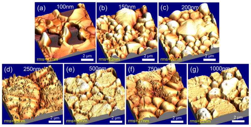
AFM measurements of as-grown Cu-Ni surfaces with copper thicknesses. As copper thin film thickness increases, top surfaces of grains become flatter but trenches in between grains become deeper. The presence of silicon impurities on each grain results in increase of roughness.
4.3 Limits of Growth on Extremely Thin Films
In order to further examine what limits of Cu-Ni thin film growth, a 50 nm copper sample with a 50 nm nickel adhesion layer was tested. Fig. 8 shows a comparison of as grown Cu-Ni thin film alloy surfaces with as-grown copper thin film surfaces for total film thicknesses of 100 nm, 500 nm, and 1000 nm. The pure copper thin films start to form voids when the thickness for the copper film decreases below 1 micron whereas the Cu-Ni alloy exhibited no dewetting of the surface until very thin films are used (t < 150 nm).
Figure 8.
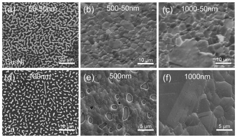
Surface dewetting comparison between Cu-Ni thin film alloys versus pure Cu thin films. (a)-(c) Cu-Ni thin film thicknesses with 50 nm Ni adhesion layers each. (d)-(f) Cu thin film thicknesses 100 nm, 500 nm, 1000 nm without Ni adhesion layer.
The Cu-Ni alloy of 50 nm/50 nm thickness also shows surface dewetting but even with the dewetting for the 50 nm/50 nm Cu-Ni film (Fig. 8(a)), it was still possible to detect the presence of monolayer graphene growth on the dewet surface as indicated by the graphene peaks found by Raman spectroscopy plotted in Fig. 9. These sparsely located graphene is presumably graphene flakes due to unstable, dewet base structure. The as-grown copper thin film of 100 nm (Fig. 8(d)) showed no such graphene peaks likely due to extremely dewet surface morphology. This is because as the copper surface dewets, the metal surface balls up causing the graphene on top of layers to flake [20]. This results in highly defective graphene that cannot easily be measured using Raman spectroscopy. Cu thin film thickness of 500 nm starts to dewet after graphene growth revealing several voids (Fig.8(b)) as Cu-Ni thin film remains stable (Fig.8(e)). There was no stability difference between Cu and Cu-Ni thin films thickness of 1000 nm in Fig.8(c) and (f).
Figure 9.
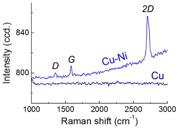
Raman spectroscopy measurement indicates that monolayer graphene flakes are randomly observed on dewet surface of 50 nm Cu/50 nm Ni thick alloy but not on pure 100 nm thick Cu film surface.
4.4 Alloying of Cu-NI Surface during Growth
To gain the insight of Ni adhesion layer, surface of Cu/Ni catalyst thin film was characterized by Time-of-Flight Secondary Ion Mass Spectrometry (TOF-SIMS) (ION-TOF GmbH), which sputters the sample surface with a focused beam of primary ions produces secondary ions, followed by further detail analysis of molecular and elemental species present in the sample as a function of the sputter depth. In the as-grown Graphene/Cu-Ni alloy samples, the TOF-SIMS analysis was preformed until the underlying SiO2 layer was reached. Fig. 10(a) exhibits the response of as-deposited 500 nm Cu/50 nm Ni thin film representing discrete layers of copper and nickel films where x-axis on the graph represents depth profile into the substrate. Higher concentration of Cu is found until 500 nm thickness profile has reached and higher concentration of Ni for 50 nm afterwards. Fig. 10(b)-(h) are depth profile of Cu-Ni thin films of thicknesses from 250 to 1000 nm each with Ni thickness of 50 nm. The profile indicates that the nickel is evenly distribute within the copper film no matter the thickness of the film after the graphene growth. The copper and nickel concentrations as a function of depth show that those two metal layers have completely formed an alloy throughout overall metal thickness for all of the films tested. The concentration of copper is almost identical regardless of its thickness, but the concentration of nickel increases as copper thickness decreases. The limited number of nickel atoms diffusing into different volumes of copper thin films is the cause of this trend. Minor nickel dispersion variation may be due to slight variations of nickel diffusivities in copper in different samples. According to our analysis in Fig. 10, carbon atoms diffuse into Cu-Ni alloy film as deep was 200 to 300 nm during graphene growth at 1000°C.
Figure 10.
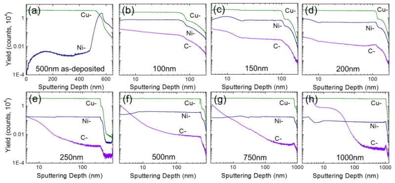
TOF-SIMS measurements of Cu-Ni samples (a) as-deposited Cu-Ni film of copper thickness of 500 nm. (b)-(h) as-grown samples with Cu-Ni alloy of copper thicknesses of 100 nm, 150 nm, 200 nm, 250 nm, 500 nm, 750 nm, and 1000 nm respectively each with 50 nm Ni, representing Cu-, Ni-, and C- counts with respect to sputtering depth. Abundant Cu- concentration remains the same with changing Cu thicknesses but Ni- concentration decreases as Cu thickness increases.
The carbon concentration near the surface of the sample was generally observed to increase as the copper thickness increased. This is due to the fact that the thicker films have more available volume for the carbon to diffuse into during growth and that when the films cool the carbon solubility decreases causing the carbon to diffuse towards the surface of the metal layer. This is consistent with the fact that the thicker layers were observed to have more multi-layer graphene growth than the thinner samples as represented in Fig. 5. Interestingly, it appears that for our range of Cu-Ni films thicknesses, film thickness has a greater effect on multi-layer graphene formation than nickel concentration. This result is somewhat unexpected given that the solubility of carbon atoms in nickel is much higher than the solubility of carbon in copper [35]. Therefore, it would be expected that multi-layer graphene would be more likely to occur in films with higher nickel alloy contents. In fact, this result is observed for Cu-Ni alloy foils [33,36]. However, it is likely that short growth time (5 min.) made carbon difficult to be absorbed into the thin film during growth to nucleate out as additional adlayers of graphene during the cooling step. Therefore, extremely thin metal catalyst films may help to promote very high levels of monolayer graphene growth regardless of the exact catalyst composition.
5 Conclusions
This paper demonstrates that monolayer graphene growth on sub-300 nm thick copper thin films is possible using a nickel adhesion layer and establishes a limit for the thickness of copper films to grow graphene. During the graphene growth, the nickel adhesion layer uniformly diffuse into the copper layer, resulting in a Cu-Ni alloy promoting large area graphene growth on extremely thin films. The nickel alloy also helps to reduce the interfacial energy between the copper and the Si/SiO2 substrate, resulting in less dewetting of the thin film catalyst surface compared to the use of single copper thin film layer. In addition, the use of thinner films helps to reduce carbon absorption into the catalyst which results in suppression of adlayer graphene formation in these Cu-Ni alloy films. Therefore, Cu-Ni thin film alloys as a metal catalyst in graphene growth suggest a promising future candidate allowing the large scale integration of graphene into nanoscale electronic and mechanical devices.
Acknowledgments
The authors would like to thank Dr. Alvin Lee for help with graphene growth, Dr. Richard Piner for AFM measurements, Dr. Andrei Dolocan for TOF-SIMS measurements and Drs. Li Tao and Deji Akinwande for their helpful discussions about these results.
Footnotes
Certain commercial equipment, instruments, or materials are identified in this article in order to specify the experimental procedure adequately. Such identification is not intended to imply recommendation or endorsement by the National Institute of Standards and Technology, nor is it intended to imply that the materials or equipment identified are necessarily the best available for the purpose.
References
- 1.Bunch JS, van der Zande AM, Verbridge SS, Frank IW, Tanenbaum DM, Parpia JM, Craighead HG, McEuen PL. Electromechanical Resonators from Graphene Sheets. Science. 2007;315 doi: 10.1126/science.1136836. (80- ) 490 LP-493. http://science.sciencemag.org/content/315/5811/490.abstract. [DOI] [PubMed] [Google Scholar]
- 2.Bolotin KI, Sikes KJ, Jiang Z, Klima M, Fudenberg G, Hone J, Kim P, Stormer HL. Ultrahigh electron mobility in suspended graphene. Solid State Commun. 2008;146:351–355. doi: 10.1016/j.ssc.2008.02.024. [DOI] [Google Scholar]
- 3.Lee C, Wei X, Kysar JW, Hone J. Measurement of the Elastic Properties and Intrinsic Strength of Monolayer Graphene. Science. 2008;321:385–388. doi: 10.1126/science.1157996. (80- ) [DOI] [PubMed] [Google Scholar]
- 4.Novoselov KS, Geim AK, Morozov SV, Jiang D, Zhang Y, Dubonos SV, Grigorieva IV, Firsov AA. Electric Field Effect in Atomically Thin Carbon Films. Science. 2004;306 doi: 10.1126/science.1102896. (80- ) 666 LP-669. http://science.sciencemag.org/content/306/5696/666.abstract. [DOI] [PubMed] [Google Scholar]
- 5.Kedzierski J, Hsu PL, Healey P, Wyatt PW, Keast CL, Sprinkle M, Berger C, de Heer Wa. Epitaxial Graphene Transistors on SiC Substrates. IEEE Trans Electron Devices. 2008;55:2078–2085. doi: 10.1109/TED.2008.926593. [DOI] [Google Scholar]
- 6.Kim KS, Zhao Y, Jang H, Lee SY, Kim JM, Ahn JH, Kim P, Choi JY, Hong BH. Large-scale pattern growth of graphene films for stretchable transparent electrodes. Nature. 2009;457:706–710. doi: 10.1038/nature07719. [DOI] [PubMed] [Google Scholar]
- 7.Li X, Cai W, An J, Kim S, Nah J, Yang D, Piner R, Velamakanni A, Jung I, Tutuc E, Banerjee SK, Colombo L, Ruoff RS. Large-area synthesis of high-quality and uniform graphene films on copper foils. Science. 2009;324:1312–1314. doi: 10.1126/science.1171245. (80- ) [DOI] [PubMed] [Google Scholar]
- 8.Hao Y, Bharathi MS, Wang L, Liu Y, Chen H, Nie S, Wang X, Chou H, Tan C, Fallahazad B, Ramanarayan H, Magnuson CW, Tutuc E, Yakobson BI, Mccarty KF, Zhang Y, Kim P, Hone J, Colombo L, Ruoff RS. The Role of Surface Oxygen in the Growth of Large Single-Crystal Graphene on Copper. Science. 2013;342 doi: 10.1126/science.1243879. (80- ) [DOI] [PubMed] [Google Scholar]
- 9.Hao Y, Wang L, Liu Y, Chen H, Wang X, Tan C, Nie S, Suk JW, Jiang T, Liang T, Xiao J, Ye W, Dean CR, Yakobson BI, Mccarty KF, Kim P, Hone J, Colombo L, Ruoff RS. Oxygen-activated growth and bandgap tunability of large single-crystal bilayer graphene. Nat Nanotechnol. 2016;11:426–431. doi: 10.1038/nnano.2015.322. [DOI] [PubMed] [Google Scholar]
- 10.Pizzocchero F, Jessen BS, Whelan PR, Kostesha N, Lee S, Buron JD, Petrushina I, Larsen MB, Greenwood P, Cha WJ, Teo K, Jepsen PU, Hone J, Boggild P, Booth TJ. Non-destructive electrochemical graphene transfer from reusable thin-film catalysts. Carbon N Y. 2015;85:397–405. doi: 10.1016/j.carbon.2014.12.061. [DOI] [Google Scholar]
- 11.Na SR, Suk JW, Tao L, Akinwande D, Ruoff RS, Huang R, Liechti KM. Selective mechanical transfer of graphene from seed copper foil using rate effects. ACS Nano. 2015;9:1325–1335. doi: 10.1021/nn505178g. [DOI] [PubMed] [Google Scholar]
- 12.Wang X, Tao L, Hao Y, Liu Z, Chou H, Kholmanov I, Chen S, Tan C, Jayant N, Yu Q, Akinwande D, Ruoff RS. Direct delamination of graphene for high-performance plastic electronics. Small. 2014;10:694–698. doi: 10.1002/smll.201301892. [DOI] [PubMed] [Google Scholar]
- 13.Tao L, Lee J, Holt M, Chou H, McDonnell SJ, Ferrer DA, Babenco MG, Wallace RM, Banerjee SK, Ruoff RS, Akinwande D. Uniform wafer-scale chemical vapor deposition of graphene on evaporated Cu (111) film with quality comparable to exfoliated monolayer. J Phys Chem C. 2012;116:24068–24074. doi: 10.1021/jp3068848. [DOI] [Google Scholar]
- 14.Tao L, Lee J, Chou H, Holt M, Ruoff RS, Akinwande D. Synthesis of high quality monolayer graphene at reduced temperature on hydrogen-enriched evaporated copper (111) films. ACS Nano. 2012;6:2319–2325. doi: 10.1021/nn205068n. [DOI] [PubMed] [Google Scholar]
- 15.Cullinan MA, Gorman JJ. Transfer-free, wafer-scale fabrication of graphene-based nanoelectromechanical resonators. MAMNA 2013 Spring Symp - Microsystems Technol Fulfilling Promise. 2013:3–6. doi: 10.1109/MAMNA.2013.6557225. [DOI] [Google Scholar]
- 16.Levendorf M, Ruiz-Vargas C, Garg S, Park J. Transfer-free batch fabrication of single layer graphene transistors. Nano Lett. 2009:1–5. doi: 10.1021/nl902790r. http://pubs.acs.org/doi/abs/10.1021/nl902790r. [DOI] [PubMed]
- 17.Han GH, Güneş F, Bae JJ, Kim ES, Chae SJ, Shin HJ, Choi JY, Pribat D, Lee YH. Influence of copper morphology in forming nucleation seeds for graphene growth. Nano Lett. 2011;11:4144–4148. doi: 10.1021/nl201980p. [DOI] [PubMed] [Google Scholar]
- 18.Van Der Zande AM, Barton RA, Alden JS, Ruiz-Vargas CS, Whitney WS, Pham PHQ, Park J, Parpia JM, Craighead HG, McEuen PL. Large-scale arrays of single-layer graphene resonators. Nano Lett. 2010;10:4869–4873. doi: 10.1021/nl102713c. [DOI] [PubMed] [Google Scholar]
- 19.Milaninia KM, Baldo MA, Reina A, Kong J. All graphene electromechanical switch fabricated by chemical vapor deposition. Appl Phys Lett. 2009;95:2–4. doi: 10.1063/1.3259415. [DOI] [Google Scholar]
- 20.Ismach A, Druzgalski C, Penwell S, Schwartzberg A, Zheng M, Javey A, Bokor J, Zhang Y. Direct chemical vapor deposition of graphene on dielectric surfaces. Nano Lett. 2010;10:1542–1548. doi: 10.1021/nl9037714. [DOI] [PubMed] [Google Scholar]
- 21.Jie S, Lindvall N, Cole MT, Angel KTT, Teng W, Teo KBK, Chua DHC, Johan L, Yurgens A. Low Partial Pressure Chemical Vapor Deposition of Graphene on Copper. Nanotechnology, IEEE Trans. 2012;11:255–260. doi: 10.1109/TNANO.2011.2160729. [DOI] [Google Scholar]
- 22.Lee YH, Lee JH. Scalable growth of free-standing graphene wafers with copper(Cu) catalyst on SiO2/Si substrate: Thermal conductivity of the wafers. Appl Phys Lett. 2010;96 doi: 10.1063/1.3324698. [DOI] [Google Scholar]
- 23.Thompson CV. Solid-State Dewetting of Thin Films. Annu Rev Mater Res. 2012;42:399–434. doi: 10.1146/annurev-matsci-070511-155048. [DOI] [Google Scholar]
- 24.Srolovitz DJ, Safran SA. Capillary instabilities in thin folms. 2: Kinetics. J Appl Phys. 1986;247:255–260. doi: 10.1063/1.337689. [DOI] [Google Scholar]
- 25.Pollard AJ, Nair RR, Sabki SN, Staddon CR, Perdigao LMA, Hsu CH, Gangopadhyay S, Gleeson HF, Geim AK, Beton PH. Formation of Monolayer Graphene by Annealing Sacricial Nickel Thin Films. J Phys. 2009:16565–16567. doi: 10.1021/jp906066z. [DOI] [Google Scholar]
- 26.Howsare CA, Weng X, Bojan V, Snyder D, Robinson JA. Substrate considerations for graphene synthesis on thin copper films. Nanotechnology. 2012;23:135601. doi: 10.1088/0957-4484/23/13/135601. [DOI] [PubMed] [Google Scholar]
- 27.Madito MJ, Bello A, Dangbegnon JK, Oliphant CJ, Jordaan WA, Momodu DY, Masikhwa TM, Barzegar F, Fabiane M, Manyala N. A dilute Cu(Ni) alloy for synthesis of large-area Bernal stacked bilayer graphene using atmospheric pressure chemical vapour deposition. J Appl Phys. 2016;119:15306. doi: 10.1063/1.4939648. [DOI] [Google Scholar]
- 28.Lee Y, Bae S, Jang H, Jang S, Zhu SE, Sim SH, Song Y Il, Hong BH, Ahn JH. Wafer-Scale Synthesis and Transfer of graphene films. Nano Lett. 2010;10:490–3. doi: 10.1021/nl903272n. [DOI] [PubMed] [Google Scholar]
- 29.Reina A, Thiele S, Jia X, Bhaviripudi S, Dresselhaus MS, Schaefer JA, Kong J. Growth of large-area single- and Bi-layer graphene by controlled carbon precipitation on polycrystalline Ni surfaces. Nano Res. 2009;2:509–516. doi: 10.1007/s12274-009-9059-y. [DOI] [Google Scholar]
- 30.Xiao K, Wu H, Lv H, Wu X, Qian H. The study of the effects of cooling conditions on high quality graphene growth by the APCVD method. Nanoscale. 2013;5:5524–9. doi: 10.1039/c3nr00524k. [DOI] [PubMed] [Google Scholar]
- 31.Keller RM, Baker SP, Arzt E. Quantitative analysis of strengthening mechanisms in thin Cu films: Effects of film thickness, grain size, and passivation. J Mater Res. 2011;13:1307–1317. doi: 10.1557/JMR.1998.0186. [DOI] [Google Scholar]
- 32.Schneider CA, Rasband WS, Eliceiri KW. NIH Image to ImageJ: 25 years of image analysis. Nat Meth. 2012;9:671–675. doi: 10.1038/nmeth.2089. http://dx.doi.org/10.1038/nmeth.2089. [DOI] [PMC free article] [PubMed] [Google Scholar]
- 33.Chen S, Cai W, Piner RD, Suk JW, Wu Y, Ren Y, Kang J, Ruoff RS. Synthesis and characterization of large-area graphene and graphite films on commercial Cu-Ni alloy foils. Nano Lett. 2011;11:3519–3525. doi: 10.1021/nl201699j. [DOI] [PubMed] [Google Scholar]
- 34.Luo Z, Lu Y, Singer DW, Berck ME, Somers LA, Goldsmith BR, Johnson ATC. Effect of substrate roughness and feedstock concentration on growth of wafer-scale graphene at atmospheric pressure. Chem Mater. 2011;23:1441–1447. doi: 10.1021/cm1028854. [DOI] [Google Scholar]
- 35.Batzill M. The surface science of graphene: Metal interfaces, CVD synthesis, nanoribbons, chemical modifications, and defects. Surf Sci Rep. 2012;67:83–115. doi: 10.1016/j.surfrep.2011.12.001. [DOI] [Google Scholar]
- 36.Liu X, Fu L, Liu N, Gao T, Zhang Y, Liao L, Liu Z. Segregation Growth of Graphene on Cu-Ni Alloy for Precise Layer Control. J Phys Chem C. 2011;115:11976–11982. [Google Scholar]


