Abstract
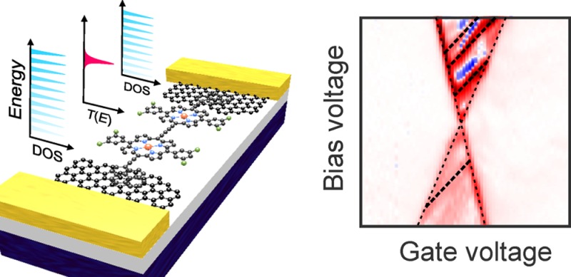
Graphene provides a two-dimensional platform for contacting individual molecules, which enables transport spectroscopy of molecular orbital, spin, and vibrational states. Here we report single-electron tunneling through a molecule that has been anchored to two graphene leads. Quantum interference within the graphene leads gives rise to an energy-dependent transmission and fluctuations in the sequential tunnel-rates. The lead states are electrostatically tuned by a global back-gate, resulting in a distinct pattern of varying intensity in the measured conductance maps. This pattern could potentially obscure transport features that are intrinsic to the molecule under investigation. Using ensemble averaged magneto-conductance measurements, lead and molecule states are disentangled, enabling spectroscopic investigation of the single molecule.
Keywords: molecular electronics, graphene, nanoelectrodes, single-electron tunneling
Graphene electrodes are advantageous for use in single-molecule devices,1−5 because unlike metal electrodes, they do not suffer from high atomic mobility and screening.1,3 Large area single-layer graphene can be grown and patterned into devices with electrodes separated by nanogaps,6,7 and molecules bridging the gap can be anchored to the electrodes via covalent bonding4 or π–π-stacking.1−3,8,9 However, the nontrivial density of states and transmission in graphene nanostructures, combined with the fact that graphene can be electrostatically gated, can lead to the observation of transport features in graphene-based single-molecule devices that are not intrinsic to the molecule under investigation, but are rather a property of the leads. Experimental and theoretical studies have shown that quantum interference in graphene ribbons10−13 and nanoconstrictions14 lead to conductance fluctuations at cryogenic temperatures. Quantum confinement in the source and drain electrodes of semiconductor single-electron transistors results in the observation of density of states oscillations in the sequential electron tunneling transport through these devices.15,16 It is therefore to be expected that quantum interference effects in graphene electrodes will also influence the charge transport in single-molecule devices.
Here we present a transport spectroscopy investigation of a graphene-based single-electron transistor where we attribute the sequential electron tunneling to the presence of a single molecule bridging the graphene nanogap. While the charge island is most likely formed by an individual zinc-porphyrin dimer, the observed transport features are completely independent of the type of molecule used, and in fact can also be observed in graphene quantum dots in a similar device geometry (see Supporting Information, where we present experimental data of zinc-porphyrin monomers and graphene quantum dots). Our experiments show how the graphene leads couple electrostatically to a global back-gate, and that hybridization between the lead and molecule states results in distinct fluctuation patterns as a function of gate and bias voltage. This behavior is captured by a simple tight-binding model, which we solve both analytically and numericially. Finally, we present a strategy to recover transport features that are intrinsic to the molecule, and might be obscured by the density of states fluctuations in the leads, by disentangling lead and molecular states.
Results and discussion
We measured charge transport in single-molecule transistors at 4.2 K (sample A) and 20 mK (sample B) as a function of bias voltage Vb and gate voltage Vg. Individual molecules were contacted using chemical vapor deposition (CVD) grown graphene nanogaps on a silicon substrate with a 300 nm thermally grown oxide layer that was prepatterned with metal (Cr/Au) contacts. The single-layer nature of the graphene was confirmed by Raman spectroscopy.14 The graphene nanogaps were fabricated using feedback-controlled electroburning.7 Single zinc-porphyrin dimer molecules were deposited from a chloroform solution, and were identified by comparing current maps as a function of Vb and Vg before and after deposition (see Supporting Information).
We have measured a total of 171 successfully electroburnt devices (meaning they were successfully burnt, did not break during the wire-bonding and cool-down procedure, and resulted in a measurable tunnel current at 77 K.) From these 171 devices, 109 were measured again at 77 K after the molecular deposition after which 26 devices appeared empty before the deposition (i.e., no Coulomb diamonds) and showed sequential tunneling after molecular deposition. We observed conductance fluctuation in 4 devices.
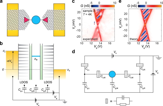
The conductance through the single zinc-porphyrin dimers was investigated via single-electron tunneling from a metallic source reservoir via the left graphene lead, through the molecule, to the metallic drain reservoir via the right graphene lead (Figure 1a). The silicon substrate was used as a backgate to apply Vg. In contrast with metal-based single-molecule transistors, where the metal electrodes screen the gate electric field, in our devices the electrostatic gating influences both the molecular orbital states and the states in the graphene leads (Figure 1b). Previous experiments using partially electroburnt graphene nanoconstrictions have shown that the transmission of our graphene leads fluctuates as a function of Vb and Vg, which we attribute to either universal conductance fluctuations (UCFs) resulting from random disorder or the presence of multimode Fabry-Pérot interferences.14 These fluctuations in the graphene leads influence the transmission through the molecule as orbital states are tuned in and out of resonance with the lead states.
Figure 1.
Measurement and theory of a graphene-based single-electron transistor. (a) Schematic depiction of the device. Graphene lead electrodes are connected to gold reservoirs left and right; a single molecule bridges the gap between the graphene electrodes. Details on the fabrication and the setup are provided in Figure S1. (b) Schematic energy diagram of the graphene–molecule–graphene junction. (c) Measured differential conductance G = dI/dVb as a function of bias and gate voltage (sample A). (d) Equivalent circuit diagram of (a) and (b); the Ohmic approximation for a tunnel barrier is valid in the low bias regime of (c) and (e). (e) Calculated differential conductance as a function of bias and gate voltage.
Figure 1c shows the differential conductance measured as a function of the applied bias and gate voltage for sample A. The data reveal a dense set of positive and negative conduction resonances visible as red and blue lines of positive slope that we attribute to fluctuations in the graphene leads. A striking feature of the data is that the red and blue lines do not run parallel to the lines at the edges of white regions of suppressed conductance. In what follows, we will discuss the origin of the conduction resonances and analyze the electrostatic gating of the molecule and the lead states.
For charge to flow through a molecule, electrons need to be added and removed from it. The energy required to add one electron to the molecule, i.e., its electron affinity, is given by the electrochemical potential μM(N) = U(N) – U(N – 1), where U(N) is the total energy of the N-electron redox state.17 This electrochemical potential consists of the discrete orbital energy plus the electrostatic contribution to the energy, which depends linearly on the source (drain) Vs(d) and gate Vg voltage as μM = −|e|(Cs,MVs + Cd,MVd + Cg,MVg)/(Cs,M + Cd,M + Cg,M), where the capacitance Cs(d,g),M describes the electrostatic interaction between the source (drain, gate) electrode and the molecule.18 Electrons can tunnel through the molecule when its electrochemical potential is within the bias window defined by the electrochemical potentials μs = −|e|Vs and μd = −|e|Vd in the source and drain reservoirs, respectively. When μd is outside this bias window, electrons do not have the necessary energy to occupy/empty an orbital, resulting in diamond-shape regions of Coulomb blockade in the conductance versus bias and gate voltage map. The slopes of these Coulomb diamonds are given by the conditions μM = μd and μM = μs. When the device is biased asymmetrically and the gate voltage is set relative to one of the electrodes, in our case the drain, i.e., Vs = Vb and Vd = 0, these conditions yield the slopes Cg,M/(Cd,M + Cg,M) and −Cg,M/Cs,M.
Similar to the molecular orbital states, the states in the graphene leads shift linearly as a function of the applied bias and gate voltage. The energy shift of the states in the left lead, which is coupled to the source reservoir, is given by ΔϵL = −|e|(Cs,LVs+Cg,LVg/(Cs,L+Cg,L), and for the right lead coupled to the drain reservoir ΔϵR = −|e|(Cd,RVd+Cg,RVg/(Cd,R+Cg,R). In the case of asymmetric biasing, lines in the conductance map for which a molecular orbital aligns with a state in the left lead have a slope given by μM = ΔϵL, which yields
| 1 |
and for states in the right lead μM = ΔϵR yields
| 2 |
When the lead states are clamped to the electrochemical potential of the reservoirs, i.e., if the capacitive coupling between the leads and the gate is zero, the slope of the lines for which the molecular orbitals align with the lead states run parallel to the edges of the Coulomb diamonds. Parallel lines in conductance maps resulting from disorder and confinement in the leads of single-electron transistors have been studied extensively, for example in STM-fabricated devices in silicon.15 However, when there is capacitive coupling between the leads and the gate, these lines no longer run parallel to the edges of the Coulomb diamonds, and resonances between molecular and lead states shift in and out of the bias window.
From the slopes of the edges of the Coulomb diamonds in Figure 1c we infer that the ratio Cg,M/Cs,M = (33 ± 1) × 10–3, and Cg,M/Cd,M = (20 ± 1) × 10–3. The relatively strong coupling to the source and drain electrodes compared to the gate electrode is due to the fact that the backgate is separated from the device by a 300 nm layer of SiO2. Next, we estimate the electrostatic coupling of the lead states to the backgate. We only observe conduction resonances with positive slopes, which implies that we predominantly probe the left lead. From the positive slope of the conduction resonances we find Cg,L/Cs,L = (7 ± 1) × 10–3, indicating that the gate coupling to the molecule is approximately 3–5 times stronger than to the lead states. We attribute the difference in gate coupling between the molecule and the lead states to the higher carrier concentration in the graphene leads, which results in a more effective screening of the gate electric field. The average spacing between the conduction resonances is approximately 5 meV, which is consistent with the conductance fluctuations we have previously observed in partially electroburnt graphene nanoconstrictions.14
We will now discuss the hybridization between the lead states and the molecular orbitals as they are tuned in and out of resonance. The current through a molecular orbital is given by the Landauer formula19
| 3 |
where fL,R denotes the Fermi distribution of the reservoirs, which in the case of asymmetric biasing depends on the bias voltage Vb and temperature T as fL = [exp((E–eVb)/kBT) + 1]−1 and fR = [exp(E/kBT) + 1]−1.
To investigate the role of scattering in the leads on the transmission through the molecular orbital we employ a simple Hückel (tight-binding) model as shown in Figure 2a. The molecule is represented by a single site at n = 0 with an on-site energy μM and a hopping integral γL,R to the left and right lead, respectively. The left and right leads are represented by semi-infinite chains with on-site energies ϵL,R and nearest-neighbor hopping integrals αL,R. We introduce scattering into the left and right compound electrodes at n = −NL and n = NR by adjusting the hopping integrals βL,R.
Figure 2.
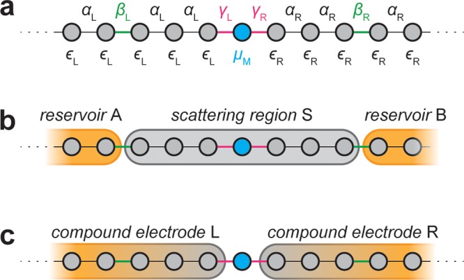
Partitioning the molecule-lead system. (a) Schematic depiction of the Hückel model. (b) Partitioning of the system into simple electrodes A and B with a complex scattering region S, and (c) into “compound electrodes” L and R and a simple scatting site M.
Traditionally one would regard this structure as a complicated scatterer (S) consisting of the region between −NL ≤ n ≤ NR (shaded gray in Figure 2b) and two simple crystalline leads (shaded orange in Figure 2b) along which electrons propagate ballistically into and from the reservoirs. For such a system,
| 4 |
where ΓA and ΓB describe the level broadening due to contact with the crystalline semi-infinite leads, A and B. In this expression, the scatterering region is a complex combination of the molecule and graphene and GSS is the Green’s function of the scattering region in the presence of the simple crystalline leads. Our aim is to separate the contributions to scattering from the molecule and graphene and therefore we adopt an alternative formulation20 in which the left graphene, and left semi-infinite lead, i.e., the region n < 0, are regarded as a compound electrode (L) and the right graphene and right semi-infinite lead (n > 0) form the right compound electrode (R). This viewpoint is encapsulated in the following alternative expression for the transmission coefficient, which is mathematically equivalent to eq 4
| 5 |
In this equation, the level broadening due to contact between the molecule and the left and right compound electrodes are described by
| 6 |
| 7 |
where gLL(RR) is the Green’s function of the isolated left(right)-hand compound electrode, and HL(R)M denotes the coupling between the left(right) compound electrode and the molecule. The Green’s function of the molecule in the presence of the compound electrodes is given by
| 8 |
where the self-energies of the left and right compound electrode are
| 9 |
| 10 |
Using eqs 5 and 6–10, we obtain the Breit–Wigner formula
| 11 |
In the case of the simple Hückel model, this implies that the tunnel-rate ΓL is proportional to the local density of states at site n = −1 and ΓR is proportional to the local density of states at site n = +1. Both the tunnel-rates and the energy shifts depend on the electrode density of states, which in turn is determined by the random locations of scattering centers within the graphene electrodes. The self-energies of the compound electrodes in the Hückel model can be found numerically by decimation (for details see Supporting Information), or analytically by solving Dyson’s equation (see Supporting Information). The latter yields
| 12 |
where xL = βL2/αL – 1 and kL = cos–1 (ϵL – E)/2α. Similarly ΓR is obtained by replacing L by R in the above expression. Here we have derived the transmission for a simple one-dimensional Hückel model, however eqs 4 and 5 are completely general, and the transmission function will depend on the details of the system Hamiltonian (see Supporting Information for a more sophisticated system Hamiltonian). Experimentally, we find that the position of the molecular energy level with respect to the Fermi energy of the leads and the strength of the coupling between the molecule and the graphene leads varies significantly from device to device.
Figure 3a,b shows the real and imaginary part of the self-energies for strong and weak reflections in the leads. For strong reflection (βL,R2 = 0.1αL,R) we find sharp peaks in the imaginary part of the self-energies, i.e., the density of states at the surface sites (n = ± 1), arising from quasi-bound states between the molecule and the reflection sites (n = −NL, NR). By contrast, for weak reflections (βL,R2 = 0.9αL,R) we find a small sinusoidal modulation of both the tunnel-rates ΓL,R and the energy shift σL,R. The tunnel-rate is maximum on resonance with the quasi-bound lead states while the hybridization energy changes sign upon crossing the resonance condition. The transmission as a function of energy and electrochemical potential of the molecule μM (Figure 3c) shows both the effect of the modulation of the tunnel-rate and the hybridization energy. The transmission is maximum upon resonance, reflecting the increase in tunnel-rate, and a avoided crossing appear around the resonance condition due to level repulsion resulting from the hybridization between the molecular orbital and the lead states.
Figure 3.
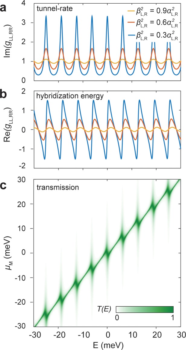
Tunnel-rate and hybridization energy. (a,b) Real and imaginary part of the surface Green’s function calculated for αL,R = 3 eV, ϵL,R = 0 eV and l = 1000. (c) Transmission as a function of energy E and on-site potential μM for γL,R = 20 meV.
To calculate the current and differential conductance as a function of bias and gate voltage as shown in Figure 1e, we introduce the experimentally extracted capacitive coupling parameters to the on-site energies as discussed in the previous section. By choosing αL,R = 1 eV and NL = NR = 1000 we obtain an energy-level spacing between the quasi-bound lead states of 2 meV, close to the observed energy spacing in our experiment. We find that choosing the hopping integrals γL = 4 μeV and γR = 20 meV results in a good qualitative agreement between the experimental and theoretical differential conductance maps. Due to strong asymmetry in coupling strength between the left and right lead, i.e. ,ΓL ≪ ΓR, the amplitude of the Breit–Wigner resonance ∼ ΓL and is only sensitive to states in the left lead.
The conductance fluctuations observed in the
sequential tunnelling
regime arise from interference effects in the leads, which can either
be the result of scattering of random impurities leading to universal
conductance fluctuations (UCFs, see Figure 4a), or Fabry-Pérot (FP, see Figure 4b) interferences
resulting from reflections at potential barriers. UCFs can be observed
if electron waves scatter along closed trajectories and the phase
coherence length lϕ is larger than
the mean free path. This scattering leads to random, energy dependent
interferences within segments of lϕ2 inside the conductor which
appear as aperiodic conductance fluctuations as a function of gate
voltage. When a magnetic field is applied perpendicular to the graphene
leads, electron waves acquire an additional phase due to the vector
potential, resulting in an Aharonov–Bohm phase ΔBAB = Φ0/S,
where Φ0 = h/e,
for a trajectory enclosing an area S. When the conductance
is measured for different magnetic fields within the correlation field
scale ΔBc ≈ Φ0/(Lx + Ly), where Lx and Ly correspond to the smallest relevant dimension in x and y direction, similar features corresponding
to a specific impurity configuration are observed in each conductance
curve.21,22 However, when the increments in external
magnetic field are larger than ΔBc, a different impurity configuration is probed for each conductance
curve. As a result, UCFs can be suppressed by ensemble averaging measurements
recorded at B > ΔBc, denoted by ⟨...⟩B. This technique
was
successfully used to distinguish between UCF and weak-localization
effects in nanowires23 and carbon nanotubes.24 Theoretically, the UCFs can be reduced by a
factor of √N where N is the
size of the ensemble.24Figure 4f shows bias traces as a function
of magnetic field recorded at Vg = 29.75
V of sample B measured at 20 mK (indicated by the dotted line in Figure 4c). We recorded 40
traces in B⊥ = Bz (Figure 4d) and 40 traces in B∥ = Bx,y (Figure 4e). For a phase coherence length lϕ ≈ 400 nm14 found
in our graphene samples ΔBc ≈ 25 mT, and therefore ΔB⊥, ΔB∥ >
ΔBc. While the out-of-plane magnetic
field changes
the conductance fluctuations (Figure 4e), the in-plane field up to 6 T does not affect the
oscillations (see Figure 4d). The fact that only the out-of-plane magnetic field influences
the conductance fluctuations further strengthens our assumption that
they are intrinsic to two-dimensional graphene leads rather than the
molecule. By comparing the conductance at B = 0 with
the data averaged over B we find a reduction of UCFs
of var(G(B = 0))/var(⟨G(B)⟩B) ≈ 6 very
close to the theoretical value of  .
.
Figure 4.
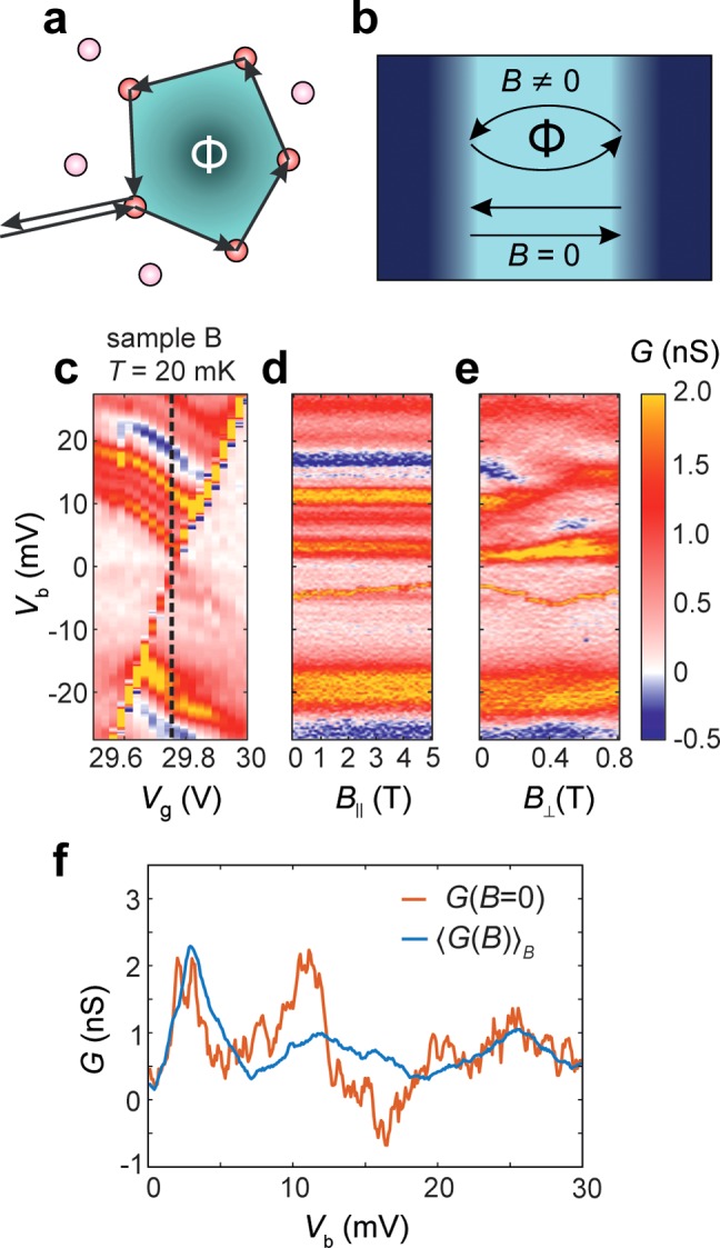
Magnetic field dependence of conductance fluctuations. (a,b) Schematic depiction of Universal Conductance Fluctuations and Fabry-Pérot interference. (c) Differential conductance map measured at B = 0 T (sample B). (d,e) Differential conductance measured as a function of bias voltage and magnetic field in (∥) and out (⊥) of the device plane. (f) Differential conductance measured at B = 0 T compared with the ensemble averaged differential conductance.
Single- and multimode
FP interference effects have previously been
observed in graphene ribbons and nanoconstrictions.14 The Lorentz force acting on the electrons in a FP cavity
will curve their trajectories when an external magnetic field is applied,
which leads to the semiclassical (kinetic) phase difference ϕWKB between two neighboring trajectories.25 In addition, bent trajectories enclosing an area S will accumulate an Aharonov–Bohm phase ϕAB = eB⊥S/ℏ = Φ/Φ0. Finally, back-reflected
electrons in graphene acquire a Berry phase ϕBerry, which is π for single-layer graphene and can take values
between 0 and 2π in bilayer graphene depending on its carrier
density and asymmetry parameter, which is defined as the difference
in on-site energies of the two graphene layers.26 Since the Berry phase is not affected by the external magnetic
field, and therefore does not play a role in magnetic-field averaging,
it can be ignored in this discussion. The resonance condition for
Fabry-Pérot interferences is met when ϕWKB + ϕAB + ϕBerry = 2πj, where  . Variations of the external magnetic field
will change this condition and thus shift the conductance maxima due
to the combined influence on ϕWKB and ϕAB (see Supporting Information).
Ensemble averaging of the magneto-conductance traces will therefore
result in the suppression of density of states fluctuations. This
behavior can be illustrated by a tight-binding model shown in Figure 5a, in which the leads
contain circular regions through which a magnetic flux can pass. Again
the transmission coefficient can be obtained analytically as a function
of the flux Φ passing through each of the loops. This is imposed
via a Peierls substitution by adding a phase factor θ = 2πΦ/Φ0 to nearest neighbor hopping integrals. In the absence of
a magnetic field, Figure 5b,c shows an example of the transmission and differential
conductance, which reflects the density of states fluctuations in
such a model. The ensemble averaged curves show a strong reduction
of the fluctuations, in correspondence with the experimental results.
Figure 5.
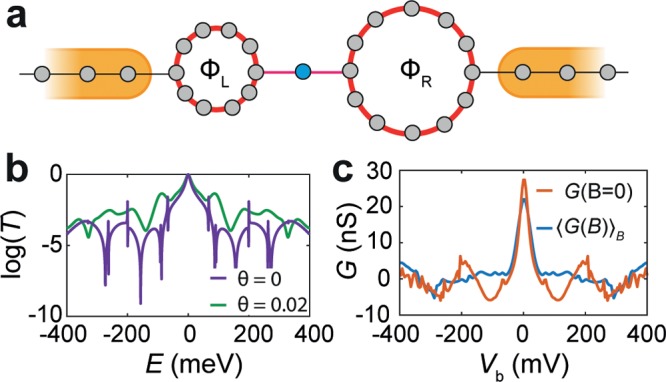
Electrodes with ring-paths. (a) Tight binding model describing a molecular orbital connected to semi-infinite one-dimensional leads via ring paths. (b) Calculated transmission for two different values of θ = 2πΦ/Φ0. (c) Differential conductance at B = 0 compared to the ensemble averaged values, calculated for αring,L = αring,R = 0.7αL,R and γL = γR = 0.075αL,R.
Conclusions
In this work we have investigated the role of density of states fluctuations in single-molecule devices contacted to single-layer graphene nanoelectrodes. By analyzing local measurements of the quasi-bound lead states, we find that the electrostatic coupling to the global back-gate is weaker than the gate coupling to the molecule. This enables electrostatic control over the hybridization between lead and molecule states. While the effect of quantum interference is in most cases detrimental to the investigation of molecular properties, because intensity variations in the conductance maps are hard to distinguish from the molecular features, it may provide a pathway toward interference-based molecular transistors. If the energy-spacing between the quasi-bound lead states can be increased by further quantum confinement, they may act as an energy filter for the transport through the molecular orbitals.27,28
Our approach of ensemble averaging magnetoconductance traces provides an effective way of distinguishing between features that are intrinsic to the molecule and those that are the result of quantum interference in the leads. This provides a useful tool for the spectroscopic investigation of single molecules, for example for the identification of vibrational states.29 However, orbital excited states are likely to shift as a function of the magnetic field due to their orbital angular momentum, and will therefore not be amenable to the ensemble averaging technique described in this work. The same holds for single-molecule magnets, which exhibit a large magnetic anisotropy. Nevertheless, the fact that the conductance lines resulting from the lead states do not run parallel to the edges of the Coulomb diamond may still be used to distinguish between lead and molecular states. In the case where magnetic ensemble averaging is not possible, e.g., when studying magnetic molecules, a coplanar gate30 could potentially reduce the effects of density of states fluctuations in the leads as it will only gate the molecule states locally.
To conclude, our results highlight the importance of the electronic properties of the lead electrodes in single-molecule electronics. While graphene may be a material system that is very well suited to host these devices, further understanding of the hybridization between graphene and molecules will be needed to develop these devices into a technology. Atomically precise control of the structure and edge termination of the graphene leads,31 together with stacked two-dimensional material approaches32 could enable functional graphene-molecule hybrid systems.
Methods
Devices are fabricated using feedback-controlled electroburning of CVD grown graphene ribbons that were wet-transferred onto a pre-patterned Si/SiO2 chip containing Au/Cr contact pads. We deposit molecules from a 10 μM chloroform solution. Devices were measured in an Oxford Instruments Triton 200 dilution refrigerator and a custom-built liquid helium dipper. Measurements were performed using low-noise, battery powered electronics. We measure the transport characteristics of the device before and after molecular deposition and select those device that only show Coulomb blockade after deposition.
Acknowledgments
This work was supported by the Clarendon Fund, the European Research Council (Grant 320969 and 606728) and the UK EPSRC (Grant EP/J015067/1 and EP/N017188/1). J.A.M. acknowledges a RAEng Research Fellowship.
Supporting Information Available
The Supporting Information is available free of charge on the ACS Publications website at DOI: 10.1021/acsnano.7b00570.
Synthesis; synthetic scheme; device fabrication; electrostatic characterization; theoretical model; additional ZnP monomer, dimer, and graphene quantum dot data; and magnetic field dependence information (PDF)
The authors declare no competing financial interest.
Supplementary Material
References
- Prins F.; Barreiro A.; Ruitenberg J. W.; Seldenthuis J. S.; Aliaga-Alcalde N.; Vandersypen L. M. K.; van der Zant H. S. J. Room-Temperature Gating of Molecular Junctions Using Few-Layer Graphene Nanogap Electrodes. Nano Lett. 2011, 11, 4607–4611. 10.1021/nl202065x. [DOI] [PubMed] [Google Scholar]
- Ullmann K.; Coto P. B.; Leitherer S.; Molina-Ontoria A.; Martín N.; Thoss M.; Weber H. B. Single-Molecule Junctions with Epitaxial Graphene Nanoelectrodes. Nano Lett. 2015, 15, 3512–3518. 10.1021/acs.nanolett.5b00877. [DOI] [PubMed] [Google Scholar]
- Mol J. A.; Lau C. S.; Lewis W. J. M.; Sadeghi H.; Roche C.; Cnossen A.; Warner J. H.; Lambert C. J.; Anderson H. L.; Briggs G. A. D. Graphene-Porphyrin Single-Molecule Transistors. Nanoscale 2015, 7, 13181–13185. 10.1039/C5NR03294F. [DOI] [PubMed] [Google Scholar]
- Jia C.; Ma B.; Xin N.; Guo X. Carbon Electrode-Molecule Junctions: A Reliable Platform for Molecular Electronics. Acc. Chem. Res. 2015, 48, 2565–2575. 10.1021/acs.accounts.5b00133. [DOI] [PubMed] [Google Scholar]
- Lumetti S.; Candini A.; Godfrin C.; Balestro F.; Wernsdorfer W.; Klyatskaya S.; Ruben M.; Affronte M. Single-Molecule Devices with Graphene Electrodes. Dalt. Trans. 2016, 45, 16570–16574. 10.1039/C6DT02445A. [DOI] [PubMed] [Google Scholar]
- Nef C.; Posa L.; Makk P.; Fu W.; Halbritter A.; Schönenberger C.; Calame M. High-Yield Fabrication of nm-Size Gaps in Monolayer CVD Graphene. Nanoscale 2014, 6, 7249–7254. 10.1039/c4nr01838a. [DOI] [PubMed] [Google Scholar]
- Lau C. S.; Mol J. a.; Warner J. H.; Briggs G. a. D. Nanoscale Control of Graphene Electrodes. Phys. Chem. Chem. Phys. 2014, 16, 20398–20401. 10.1039/C4CP03257H. [DOI] [PubMed] [Google Scholar]
- Péterfalvi C. G.; Lambert C. J. Suppression of Single-Molecule Conductance Fluctuations Using Extended Anchor Groups on Graphene and Carbon-Nanotube Electrodes. Phys. Rev. B: Condens. Matter Mater. Phys. 2012, 86, 85443. 10.1103/PhysRevB.86.085443. [DOI] [Google Scholar]
- Bailey S.; Visontai D.; Lambert C. J.; Bryce M. R.; Frampton H.; Chappell D. A Study of Planar Anchor Groups for Graphene-Based Single-Molecule Electronics. J. Chem. Phys. 2014, 140, 054708. 10.1063/1.4861941. [DOI] [PubMed] [Google Scholar]
- Gunlycke D.; White C. T. Graphene Interferometer. Appl. Phys. Lett. 2008, 93, 122106. 10.1063/1.2988825. [DOI] [Google Scholar]
- Oksanen M.; Uppstu A.; Laitinen A.; Cox D. J.; Craciun M. F.; Russo S.; Harju A.; Hakonen P. Single-Mode and Multimode Fabry-Pérot Interference in Suspended Graphene. Phys. Rev. B: Condens. Matter Mater. Phys. 2014, 89, 121414. 10.1103/PhysRevB.89.121414. [DOI] [Google Scholar]
- Bischoff D.; Libisch F.; Burgdörfer J.; Ihn T.; Ensslin K. Characterizing Wave Functions in Graphene Nanodevices: Electronic Transport Through Ultrashort Graphene Constrictions on a Boron Nitride Substrate. Phys. Rev. B: Condens. Matter Mater. Phys. 2014, 90, 115405. 10.1103/PhysRevB.90.115405. [DOI] [Google Scholar]
- Sadeghi H.; Mol J. a.; Lau C. S.; Briggs G. A. D.; Warner J.; Lambert C. J. Conductance Enlargement in Picoscale Electroburnt Graphene Nanojunctions. Proc. Natl. Acad. Sci. U. S. A. 2015, 112, 2658–2663. 10.1073/pnas.1418632112. [DOI] [PMC free article] [PubMed] [Google Scholar]
- Gehring P.; Sadeghi H.; Sangtarash S.; Lau C. S.; Liu J.; Ardavan A.; Warner J. H.; Lambert C. J.; Briggs G. A. D.; Mol J. A. Quantum Interference in Graphene Nanoconstrictions. Nano Lett. 2016, 16, 4210–4216. 10.1021/acs.nanolett.6b01104. [DOI] [PubMed] [Google Scholar]
- Fuechsle M.; Mahapatra S.; Zwanenburg F. A.; Friesen M.; Eriksson M. A.; Simmons M. Y. Spectroscopy of Few-Electron Single-Crystal Silicon Quantum Dots. Nat. Nanotechnol. 2010, 5, 502–505. 10.1038/nnano.2010.95. [DOI] [PubMed] [Google Scholar]
- Escott C. C.; Zwanenburg F. A.; Morello A. Resonant Tunnelling Features in Quantum Dots. Nanotechnology 2010, 21, 274018. 10.1088/0957-4484/21/27/274018. [DOI] [PubMed] [Google Scholar]
- Perrin M. L.; Burzurí E.; van der Zant H. S. J. Single-Molecule Transistors. Chem. Soc. Rev. 2015, 44, 902–919. 10.1039/C4CS00231H. [DOI] [PubMed] [Google Scholar]
- Hanson R.; Petta J. R.; Tarucha S.; Vandersypen L. M. K.; Kouwenhoven L. P. Spins in Few-Electron Quantum Dots. Rev. Mod. Phys. 2007, 79, 1217–1265. 10.1103/RevModPhys.79.1217. [DOI] [Google Scholar]
- Lambert C. J. Basic Concepts of Quantum Interference and Electron Transport in Single-Molecule Electronics. Chem. Soc. Rev. 2015, 44, 875–888. 10.1039/C4CS00203B. [DOI] [PubMed] [Google Scholar]
- Sangtarash S.; Huang C.; Sadeghi H.; Sorohhov G.; Hauser J.; Wandlowski T.; Hong W.; Decurtins S.; Liu S.-X.; Lambert C. J. Searching the Hearts of Graphene-like Molecules for Simplicity, Sensitivity, and Logic. J. Am. Chem. Soc. 2015, 137, 11425–11431. 10.1021/jacs.5b06558. [DOI] [PubMed] [Google Scholar]
- Lee P. A.; Stone A. D.; Fukuyama H. Universal Conductance Fluctuations in Metals: Effects of Finite Temperature, Interactions, and Magnetic Field. Phys. Rev. B: Condens. Matter Mater. Phys. 1987, 35, 1039–1070. 10.1103/PhysRevB.35.1039. [DOI] [PubMed] [Google Scholar]
- Li Z.; Chen T.; Pan H.; Song F.; Wang B.; Han J.; Qin Y.; Wang X.; Zhang R.; Wan J.; et al. Two-Dimensional Universal Conductance Fluctuations and the Electron-Phonon Interaction of Surface States in Bi2Te2Se Microflakes. Sci. Rep. 2012, 2, 1–5. 10.1038/srep00595. [DOI] [PMC free article] [PubMed] [Google Scholar]
- Petersen G.; Hernández S. E.; Calarco R.; Demarina N.; Schäpers T. Spin-Orbit Coupling and Phase-Coherent Transport in InN Nanowires. Phys. Rev. B: Condens. Matter Mater. Phys. 2009, 80, 125321. 10.1103/PhysRevB.80.125321. [DOI] [Google Scholar]
- Man H. T.; Morpurgo A. F. Sample-Specific and Ensemble-Averaged Magnetoconductance of Individual Single-Wall Carbon Nanotubes. Phys. Rev. Lett. 2005, 95, 026801. 10.1103/PhysRevLett.95.026801. [DOI] [PubMed] [Google Scholar]
- Young A. F.; Kim P. Quantum Interference and Klein Tunnelling in Graphene Heterojunctions. Nat. Phys. 2009, 5, 222–226. 10.1038/nphys1198. [DOI] [Google Scholar]
- Varlet A.; Liu M.-h.; Krueckl V.; Bischoff D.; Simonet P.; Watanabe K.; Taniguchi T.; Richter K.; Ensslin K.; Ihn T. Fabry-Pérot Interference in Gapped Bilayer Graphene with Broken Anti-Klein Tunneling. Phys. Rev. Lett. 2014, 113, 1–5. 10.1103/PhysRevLett.113.116601. [DOI] [PubMed] [Google Scholar]
- Oroszlány L.; Kormányos A.; Koltai J.; Cserti J.; Lambert C. J. Nonthermal Broadening in the Conductance of Double Quantum Dot Structures. Phys. Rev. B: Condens. Matter Mater. Phys. 2007, 76, 045318. 10.1103/PhysRevB.76.045318. [DOI] [Google Scholar]
- Li Y.; Mol J. A.; Benjamin S. C.; Briggs G. A. D. Interference-Based Molecular Transistors. Sci. Rep. 2016, 6, 33686. 10.1038/srep33686. [DOI] [PMC free article] [PubMed] [Google Scholar]
- Lau C. S.; Sadeghi H.; Rogers G.; Sangtarash S.; Dallas P.; Porfyrakis K.; Warner J.; Lambert C. J.; Briggs G. A. D.; Mol J. A. Redox-Dependent Franck-Condon Blockade and Avalanche Transport in a Graphene-Fullerene Single-Molecule Transistor. Nano Lett. 2016, 16, 170–176. 10.1021/acs.nanolett.5b03434. [DOI] [PubMed] [Google Scholar]
- Puczkarski P.; Gehring P.; Lau C. S.; Liu J.; Ardavan A.; Warner J. H.; Briggs G. A. D.; Mol J. a. Three-terminal Graphene Single-Electron Transistor Fabricated Using Feedback-Controlled Electroburning. Appl. Phys. Lett. 2015, 107, 133105. 10.1063/1.4932133. [DOI] [Google Scholar]
- Verzhbitskiy I. A.; Corato M. D.; Ruini A.; Molinari E.; Narita A.; Hu Y.; Schwab M. G.; Bruna M.; Yoon D.; Milana S.; et al. Raman Fingerprints of Atomically Precise Graphene Nanoribbons. Nano Lett. 2016, 16, 3442–3447. 10.1021/acs.nanolett.5b04183. [DOI] [PMC free article] [PubMed] [Google Scholar]
- Calado V. E.; Goswami S.; Nanda G.; Diez M.; Akhmerov A. R.; Watanabe K.; Taniguchi T.; Klapwijk T. M.; Vandersypen L. M. K. Ballistic Josephson Junctions in Edge-Contacted Graphene. Nat. Nanotechnol. 2015, 10, 761–764. 10.1038/nnano.2015.156. [DOI] [PubMed] [Google Scholar]
Associated Data
This section collects any data citations, data availability statements, or supplementary materials included in this article.


