Abstract
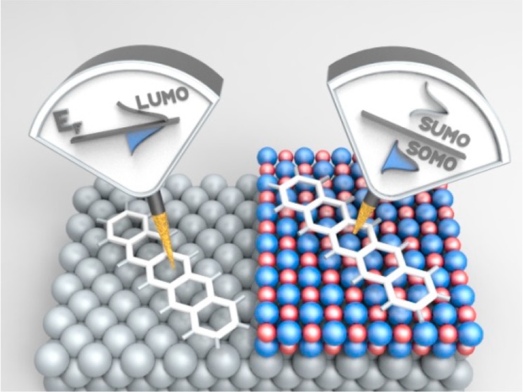
It is becoming accepted that ultrathin dielectric layers on metals are not merely passive decoupling layers, but can actively influence orbital energy level alignment and charge transfer at interfaces. As such, they can be important in applications ranging from catalysis to organic electronics. However, the details at the molecular level are still under debate. In this study, we present a comprehensive analysis of the phenomenon of charge transfer promoted by a dielectric interlayer with a comparative study of pentacene adsorbed on Ag(001) with and without an ultrathin MgO interlayer. Using scanning tunneling microscopy and photoemission tomography supported by density functional theory, we are able to identify the orbitals involved and quantify the degree of charge transfer in both cases. Fractional charge transfer occurs for pentacene adsorbed on Ag(001), while the presence of the ultrathin MgO interlayer promotes integer charge transfer with the lowest unoccupied molecular orbital transforming into a singly occupied and singly unoccupied state separated by a large gap around the Fermi energy. Our experimental approach allows a direct access to the individual factors governing the energy level alignment and charge-transfer processes for molecular adsorbates on inorganic substrates.
Keywords: integer charge transfer, energy level alignment, ultrathin films, orbital tomography, scanning tunneling microscopy, pentacene, magnesium oxide
Thin dielectric layers on metals form the basis for many applications such as semiconductor microelectronics, corrosion protection, or data read-out (magnetic tunnel junctions), but are also of interest in fundamental research. On the one hand, various potentially interesting phenomena can arise from the reduced thickness and the variability of composition and structure in the ultrathin regime, leading to drastically changed chemical and physical properties compared to the corresponding bulk-like analogs.1,2 On the other hand, the possibility to simply electronically decouple adsorbed species from the metallic substrate has allowed fundamental atomic and molecular properties, such as the imaging of orbitals and the charge-state switching of atoms and molecules by scanning tunneling microscopy (STM)3−5 or the observation of giant magnetic anisotropy and long magnetization lifetime of single atom magnets,6 to be studied. However, thin dielectric layers on metal surfaces can play a far more active role than mere decoupling or passivating layers. Large changes in work function (WF) induced by the dielectric can change the electron energy level alignment for adsorbates such that charge transfer is promoted.7,8 This phenomenon can have important consequences in fields ranging from catalysis to organic electronics.9−13
The basic concepts of energy level alignment at, and of charge transfer across, the interfaces are generally understood. As the interaction between adsorbates and (large band gap) dielectrics is in general weak, the dominant charge-transfer mechanism from the substrate through the dielectric into the adsorbate is tunneling, in which case the transferred charge is expected to be integer. This has to be distinguished from fractional charge transfer, which occurs in strongly coupled (hybridized) systems, e.g., for adsorbates in direct contact with a metal. However, the quantification of transferred charge is challenging, both theoretically and experimentally. For instance, the degree of calculated charge transfer is strongly dependent on the functional used and on the computational scheme employed to quantify charges in density functional theory (DFT) calculations.14 Experimentally, while the presence of charged species can be inferred from optical spectroscopy or STM,4,15,16 it cannot be quantified. Ultraviolet photoemission spectroscopy (UPS) can give direct access to charge-transfer states. However, without unambiguous identification of emission features to orbitals, charge transfer is difficult to infer, and without an understanding of the photoemission angular distribution, until now, it is impossible to quantify.17 Moreover, from the properties known for the isolated substrate and adsorbate, which typically are the WF of the substrate and the electron affinity (EA) and ionization potential (IP) of the adsorbate, one can generally not conclude whether or not charge transfer will occur. Additional contributions that govern the energetic position of the molecular orbitals upon adsorption, and usually come hand-in-hand, are the polarizability of the substrate and Pauli repulsion (push-back effect).18 While the former reduces the gap between frontier orbitals (increasing EA and decreasing IP), the push-back effect reduces the WF of the system and thereby the overall energy level alignment.19
In the present work, we aim at an experimental quantification of both charge transfer across interfaces and energy level alignment at interfaces characterized by strong and weak electronic coupling. To this end, we use as a model the organic semiconductor pentacene adsorbed on pristine Ag(001) and the same substrate covered by an ultrathin dielectric layer, respectively. The atomic structure and the shape of the frontier orbitals of adsorbed pentacene (5A, C22H14) (Figure 1a) have already been experimentally resolved with atomic force microscopy and STM, respectively.3,20−22 STM in particular allows the frontier orbitals to be identified. This often requires that the molecule is electronically decoupled from the metallic substrate, which can be achieved, for example, by adsorbing 5A on ultrathin NaCl layers grown on Cu(111).3 This substrate system exhibits a comparably high WF and the molecule remains uncharged on the surface. Herein, we study the integer charge-transfer state of 5A, which is spontaneously formed by occupation of the lowest unoccupied molecular orbital (LUMO) of 5A on the electronically decoupling, low-WF substrate system of ultrathin MgO(001) films on Ag(001) (Figure 1b). We compare the charging behavior of 5A on this substrate with the charge transfer on 5A/Ag(001) without dielectric interlayer and will show that the presence of the dielectric, at first glance counterintuitively, promotes charge transfer to 5A. Moreover, we will present direct evidence for integer charge occupation of the LUMO by imaging orbitals in real and reciprocal space via STM and photoemission tomography, respectively, which enables us to unambiguously identify the singly occupied (SOMO) and the associated unoccupied (SUMO) molecular orbital of the molecule.
Figure 1.
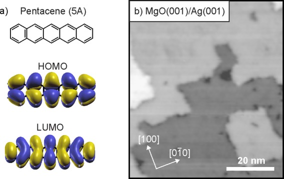
(a) Chemical structure and shape of the frontier orbitals of pentacene, 5A. (b) STM image (75 nm × 65 nm) of 2 ML MgO(001)/Ag(001) (Usample = 3.2 V, it = 100 pA).
Results and Discussion
Charge Transfer into Pentacene
As the WF prior to adsorption of the molecule is the principal driving force for the charge transfer to the molecule, and the final WF after adsorption depends on the degree of charge transfer to the molecule, an indication about the charge flow can be obtained from WF changes (Table 1). Upon adsorption of a full monolayer (ML) 5A, the WF of the bare Ag(001) surface, 4.3 eV, is decreased by 0.4 eV. This change arises from the reduction of the WF by the push-back of the electrons spilling out from the Ag(001) surface (Pauli repulsion), which is partly compensated by the dipole induced by charge transfer to the molecular layer.
Table 1. Experimental and Calculated WFs Φ and WF Changes ΔΦ for Adsorption of 5A on Bare Ag(001) and 2 ML MgO(001)/Ag(001).
| Φexp (Φtheo), eV | ΔΦexp (ΔΦtheo), eV | |
|---|---|---|
| Ag(001) | 4.3(4.28) | |
| 5A/Ag(001) | 3.9(3.91) | –0.4(−0.37) |
| Ag(001) | 4.3(4.28) | |
| 2 ML MgO(001)/Ag(001) | 2.6(3.04) | –1.7(−1.24) |
| 5A/2 ML MgO(001)/Ag(001) | 3.8(3.78) | +1.2(+0.74) |
For a 2 ML thin MgO film on Ag(001), our measurements confirm previous theoretical and experimental results,23−25 showing a 1.7 eV reduction of the WF upon dielectric film formation. The large reduction in WF is due to the push-back, which is uncompensated as there is no significant net charge transfer to the MgO layer. Subsequent adsorption of a full monolayer of 5A on MgO(001)/Ag(001) leads to an increase of the WF by 1.2 eV. This increase can be explained by charge transfer and the corresponding induced dipole caused by the presence of negatively charged molecules on the MgO surface. Note that the final WFs of 5A/Ag(001) and 5A/MgO(001)/Ag(001) are essentially the same, suggesting Fermi level pinning in both cases.26
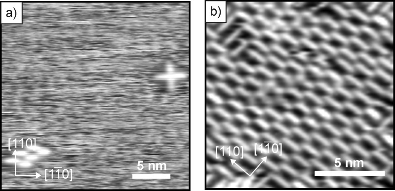
The observed WF changes (Table 1) support the idea of spontaneous charging of 5A by occupation of 5A’s LUMO upon adsorption on 2 ML MgO(001)/Ag(001). To gain molecular information about the adsorption and charging of 5A on Ag(001) and MgO(001)/Ag(001), the systems were analyzed with STM. Figure 2a shows a representative STM image of a submonolayer coverage of 5A on bare Ag(001). The 5A molecules are in general very mobile on the metallic substrate at 77K, as indicated by the noisy appearance of the image. Only occasionally clusters of stable, immobile molecules were found on flat Ag(001) terraces (e.g., four molecules forming the cross on the upper right corner, and the cluster of six molecules on the left side in Figure 2a) and at step edges. Upon increasing the coverage of 5A on Ag(001) to a full monolayer, the molecules are immobilized in ordered domains with their long molecular axis aligned parallel to the principal [110]/[11̅0] directions (Figure 2b). Note that the molecules usually appear as rod-like protrusions in both filled- and empty-state images. Occasionally, orbital-like structure was resolved on these surfaces, possibly when the STM tip got unintentionally functionalized with a 5A molecule.
Figure 2.
STM of (a) submonolayer coverage and (b) monolayer coverage of 5A on Ag(001). (a) Usample = −0.8 V, it = 90 pA, 25 nm × 25 nm; (b) Usample = −0.6 V, it = 50 pA, 13.5 nm × 13.5 nm.
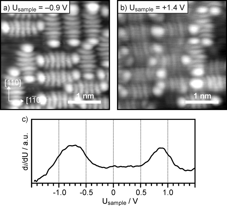
STM images of submonolayer coverages of 5A molecules on 2 ML MgO(001)/Ag(001) thin films are shown in Figure 3a,b, respectively. In contrast to clean Ag(001), the molecules are immobile, even at submonolayer coverage. They are again aligned, because of the [100]/[100] epitaxial relationship between Ag(001) and MgO(001), with their long axis parallel to the principal [110]/[11̅0] directions, i.e., along the closed-packed Mg/O rows of the film. The molecules display a distinct orbital-like structure at the bias voltages applied. All 5A molecules feature a 7-lobe structure, clearly resembling the LUMO of isolated 5A (Figure 1a),3 when imaged at Usample ≈1 V both below (Figure 3a) and above EF (Figure 3b). Representative STS spectra (Figure 3c) reveal the presence of two states at Usample = −0.8 V and Usample = +0.9 V, which both have, according to the images shown in Figure 3a,b, LUMO-like character. Observation of the LUMO shape below EF proves charge transfer into the 5A molecules, while the appearance of the LUMO above EF indicates that the LUMO is not fully occupied. One would naturally conclude from this result that the two states observed in STS correspond, respectively, to the singly occupied (SOMO, below EF) and its associated unoccupied (SUMO, above EF) molecular orbital state of the molecule. At this point, we have to mention that qualitatively comparable results have been reported for a neutral Au–5A complex created on 3 ML NaCl/Cu(111), where similar submolecular structures are observed above and below EF. However, there the splitting was attributed to temporary charging and discharging of the neutral molecule by the STM tip.27
Figure 3.
STM (3.3 nm × 3.3 nm, it = 20 pA) of submonolayer coverage of 5A on 2 ML MgO(001)/Ag(001) thin films. (a) Filled-state and (b) empty-state images obtained at a sample bias of −0.9 V and +1.4 V, respectively. (c) STS spectrum of 5A on 2 ML MgO(001)/Ag(001).
Since STM alone obviously does not allow to unambiguously conclude the electronic structure of the system, we performed ab initio calculations within the framework of density functional theory (DFT) and additional photoemission imaging and spectroscopy experiments to gain further insight into the charge rearrangement, electronic structure, and energy level alignment of the 5A/MgO(001)/Ag(001) (and 5A/Ag(001)) interface.
DFT Calculations
Two types of calculations were considered: one for 5A adsorbed on Ag(001) and MgO(001)/Ag(001), utilizing the VASP code,28,29 and another one for gas-phase 5A, using the NWChem package.30
On both surfaces, the calculations confirm the experimental findings of the molecules being aligned along the [110]/[11̅0] substrate directions and of charge transfer into the molecules. First, consider the situation for 5A adsorbed on clean Ag(001). The 5A molecule adsorbs on-top of the closed-packed Ag row with the central benzene unit centered on a Ag atom (Figure 4a) and a calculated adsorption energy of 2.65 eV/molecule. Information about charge transfer and charge rearrangement upon adsorption is gained from the charge density differences shown in Figure 4b and the projected density of states (PDOS) plotted in Figure 4c. Similar to 5A adsorbed on Ag(110),31 the energetic position of the molecular LUMO falls onto EF (Figure 4c), indicating charge transfer into 5A and partial occupation of the LUMO. This can also directly be seen in the charge density difference plot, which indicates that charge accumulation (red) at the molecule occurs at locations that resemble the shape of the LUMO (Figure 4b, horizontal cut). However, there is also considerable charge depletion (blue) from the molecule, which shows that deeper lying molecular orbitals donate charge to the molecule–substrate bond.32 The strong Pauli repulsion between the π electrons of 5A and the electrons of the Ag substrate is represented in the vertical cut in Figure 4b by the charge depletion layer directly above the topmost Ag atoms. The excellent agreement between experimental and calculated WFs for this weakly hybridized molecule–substrate system (Table 1) strongly suggests that the calculation correctly reproduces the effects of charge transfer and push-back in this system.
Figure 4.
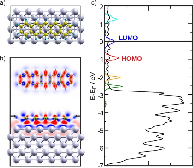
(a) Top view of the most stable adsorption configuration of 5A on Ag(001) (Ag: light gray; C: gold; H: light blue). (b) Horizontal (top) and vertical two-dimensional cuts showing the charge density differences induced by 5A adsorption on the Ag(001) substrate. The arrows indicate where the horizontal cut has been made. Red shows accumulation and blue depletion of charge, respectively. (c) PDOS obtained for the 5A/Ag(001) interface using the GGA functional. The DOS projected onto the Ag atoms (black) has been reduced for better visibility. In addition, the projections on the molecular orbitals are shown for LUMO+1 (cyan), LUMO (blue), HOMO (red), HOMO–1 (orange), and HOMO–2 (dark green).
We now turn to 5A on the 2 ML MgO(001)/Ag(001) films. Here, the most stable adsorption configuration is flat-lying on top of the oxygen rows (Figure 5a). In contrast to the bare Ag(001) surface, where potential barriers <0.1 eV for the lateral movement of 5A have been calculated, the potential barriers are increased by 0.6 eV on the MgO thin film. This immobilization can be understood when considering the calculated charge density differences depicted in Figure 5b. These show an accumulation of charge beneath the benzene rings, directed toward the Mg2+ ions beneath the molecule. Thus, there is a strong dipolar contribution to the bonding, and the molecule gets locked into the positions of the cations. Note that this is also reflected in the considerably enhanced adsorption energy of 4.71 eV/molecule compared to 5A/Ag(001) (2.65 eV). The substantially increased diffusion barrier is in accordance with STM observations of reduced mobility of submonolayer coverages of 5A on MgO(001)/Ag(001) compared to Ag(001) (at 77 K).
Figure 5.
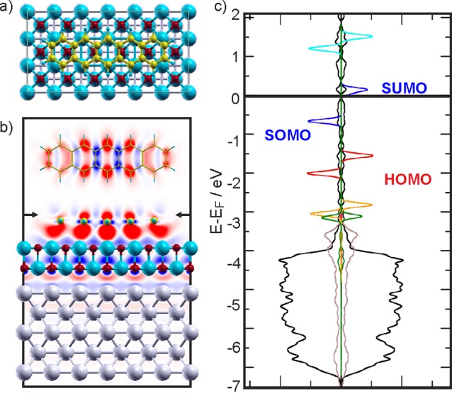
(a) Top view of the most stable adsorption configuration of 5A on 2 ML MgO(001)/Ag(001) (Ag: light gray; O: red; Mg: blue; C: gold; H: light blue). (b) Horizontal (top) and vertical two-dimensional cuts showing the charge density differences induced by 5A adsorption on the 2 ML MgO(001)/Ag(001) substrate. The arrows indicate where the horizontal cut has been made. Red shows accumulation and blue depletion of charge, respectively. (c) Spin-resolved PDOS obtained for the 5A/MgO(001)/Ag(001) interface using the HSE functional. The DOS projected onto the MgO (brown) and Ag (black) has been reduced for better visibility. In addition, the projections on the molecular orbitals are shown for LUMO+1 (cyan), LUMO (blue), HOMO (red), HOMO–1 (orange), and HOMO–2 (dark green).
The charge density difference plot (Figure 5b) also shows a charge accumulation above the molecular backbone, which again resembles the shape of the molecule’s LUMO, and naturally suggests charge transfer into the LUMO. Note that the calculated WF change resulting from the charge rearrangement in the system upon 5A adsorption is in good agreement with the experimentally determined WF change (Table 1). In addition, we mention that the presence of the charged 5A molecule induces similar effects in the MgO layer as other charged species, e.g. Au, including the buildup of a polarization in vertical direction (as seen in Figure 5b) and a polaronic distortion of the MgO lattice, which is a necessary factor for the stabilization of charged species above the dielectric film.33,34
The spin-resolved density of states calculated using the Heyd–Scuseria–Ernzerhof (HSE) functional,35 corresponding to the situation discussed above, is shown in Figure 5c. Clearly, and in contrast to the 5A/Ag(001) system, a distinct spin split of the former LUMO states (blue lines) below and above the Fermi level is observed. Consequently, the two states, which both have the shape of the LUMO, can be assigned as SOMO and SUMO states. As such, the PDOS further supports the conclusion, drawn from the experimental results, of charge transfer into 5A. However, the energy gap of 0.8 eV between the two spin states is undoubtedly underestimated due to the incorrect asymptotic behavior of the HSE potential. Note that this problem is far worse when using a standard GGA functional, which results in the LUMO straddling EF with an almost imperceptible difference between spin-up and spin-down energies.
In order to obtain a better estimation for the SOMO–SUMO gap, we have calculated the electronic structure of an isolated molecule using an optimally tuned range-separated hybrid (OT-RSH) functional.36 OT-RSH calculations are known to be useful for correcting the severe underestimation of gaps between occupied and unoccupied states inherent in DFT calculations.36−38 For neutral 5A, the calculated EA and IP of 1.4 and 6.3 eV (gap 4.9 eV)38,39 are in good agreement with gas-phase experimental results of 1.4 and 6.6 eV (gap 5.2 eV). The OT-RSH calculation for the singly charged 5A anion yields a SOMO–SUMO gap of 3.9 eV. Naturally, in the solid state, the polarizability of the environment will decrease the IP and increase the EA and thus reduce the band gap,39−42 which can be empirically estimated: As shown further below, the measured IP of the 5A HOMO on the MgO(001)/Ag(001) surface is 5.7 eV, thus 0.9 eV lower than that of the gas phase, and, as an increase similar in magnitude can be expected for the EA (see Supporting Information), a gap reduction of 1.8 eV is estimated. By taking this into account, the predicted SOMO–SUMO gap is reduced to 2.1 eV, in closer agreement with the gap measured with STS (1.7 eV).
Quantification of Charge Transfer
While the STM and DFT results are qualitatively in agreement, the unambiguous identification of the states observed in STM/STS may be problematic, owing to a possible influence of the tip, and the questions regarding the degree of charge transfer and the energy level alignment remain open. Photoemission tomography, the analysis of the angular photoemission distribution within the plane wave final-state approximation, has been demonstrated to be a quantitative tool to identify photoemission features and orbital energy ordering,43,44 deduce the molecular orientation, and even reconstruct real space orbitals of adsorbed molecules.40,45,46
The simulations for the photoemission distribution from the HOMO and LUMO of two orthogonally oriented, flat lying 5A molecules are shown in comparison to experimental momentum maps obtained from a monolayer of 5A on pristine Ag(001) and on 2 ML MgO(001)Ag(001), respectively, at binding energies where the emissions of the molecule-induced states appear (Figure 6a). We first note that in both, the resemblance of simulated and measured HOMO and LUMO intensity distributions is clear. Thus, the emissions are identified as HOMO and LUMO states, and, in agreement with STM, the molecules are concluded to lie flat and parallel to the [110]/[11̅0] azimuths. Furthermore, detection of the LUMO below EF (EB = 0.3 eV for 5A/Ag(001) and EB = 0.8 eV for 5A/MgO(001)/Ag(001)) immediately confirms that charge transfer into the molecule occurs on both substrates.
Figure 6.
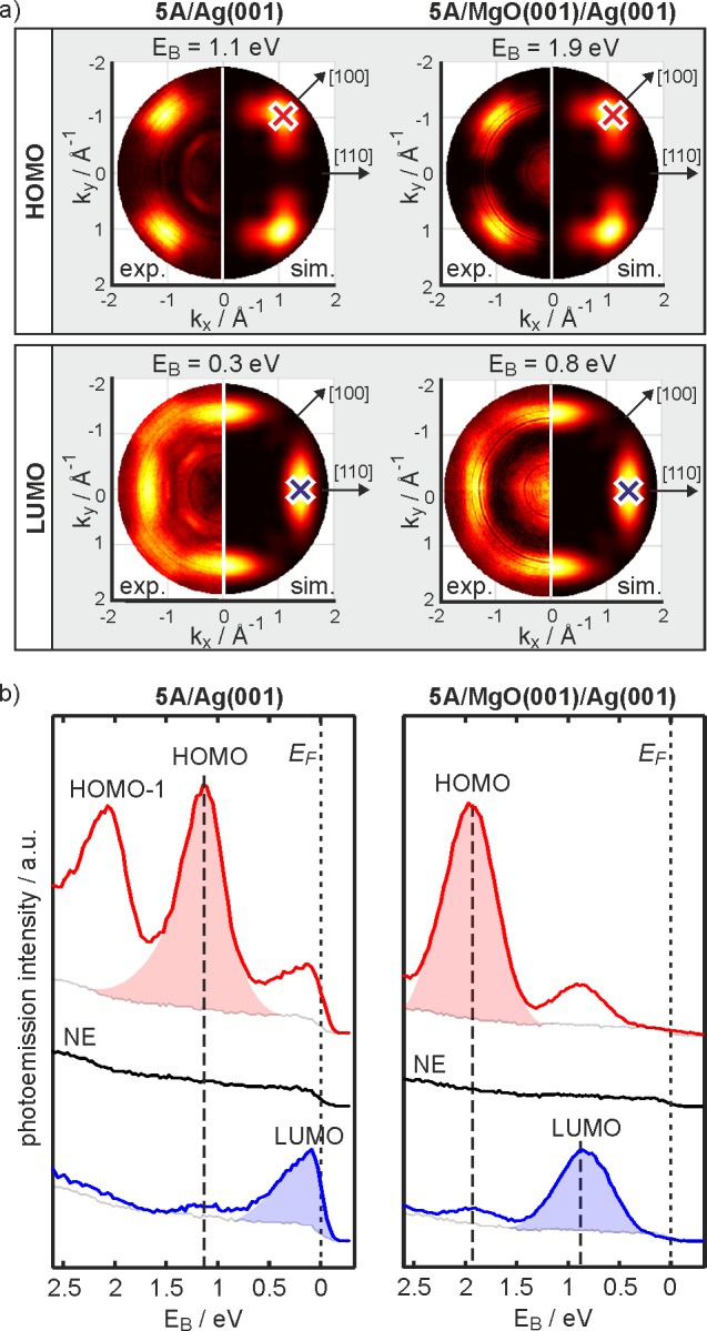
ARPES of 5A monolayer coverage on Ag(001) (left column) and on 2 ML MgO(001)/Ag(001) (right column). (a) Momentum maps of the HOMO (top row) and the LUMO (second row) emission features. Theoretical results for two isolated 5A molecules with perpendicular orientations (right halves of momentum maps) are compared to the experimentally obtained data (left halves of momentum maps) at the stated binding energies, EB. (b) ARPES spectra of 5A/Ag(001) (left column) and 5A/MgO(001)/Ag(001) (right column) measured at k positions of the HOMO(red)/LUMO(blue) intensity maxima in the momentum maps (depicted as red/blue crosses in panel (a)). Normal emission (NE) spectra are shown for comparison (black). The peak areas of the HOMO/LUMO emission features are depicted as red and blue shadings.
To better quantify the energies and intensities of the emission features, angle-resolved spectra were obtained with a goniometer-mounted electron spectrometer. Spectra at normal emission (kx = ky = 0) and at the emission directions where the HOMO and LUMO intensities are maximized (red and blue crosses in Figure 6a) are displayed in Figure 6b for 5A/Ag(001) and 5A/MgO(001)/Ag(001), respectively. For 5A on Ag(001), as predicted by the simulation, no molecular features are observed in normal emission, and only the Ag(001) Fermi edge is visible. At the geometry of the HOMO emission maximum, two peaks are visible corresponding to the HOMO–1 (EB = 2.07 eV) and the HOMO (EB = 1.14 eV), while for the LUMO geometry, only an enhancement at the Fermi edge is observed.
For 5A/MgO(001)/Ag(001), again no molecular features are visible in normal emission, and the intensity at the Fermi edge is diminished compared to 5A/Ag(001), indicating a well-established MgO interlayer. At emission directions characteristic for the HOMO and LUMO, the HOMO is found at EB = 1.94 eV, shifted down by 0.8 eV relative to 5A on Ag(001), and the LUMO is now a distinct emission feature well below the Fermi edge at EB = 0.81 eV.
Qualitatively, and somewhat counterintuitively, the peak area of the LUMO emission has increased substantially due to the introduction of the MgO dielectric layer. At the emission geometries of Figure 6b, the plane wave final-state simulations predict a HOMO/LUMO intensity ratio of 1.26 given the orbitals have the same occupation. With the not unreasonable assumption that the HOMO occupancy is 2 electrons, the relative experimental peak areas of the emissions (depicted as shaded blue and red areas in Figure 6b) can be used to estimate the LUMO filling. For 5A/Ag(001), a LUMO occupancy of 0.7 e per molecule is concluded. Fractional charge transfer is also indicated by the truncated appearance of the LUMO emission at EF in Figure 6b. This indicates hybridization of the molecular LUMO with states of the Ag(001) substrate.
Comparing the measured HOMO/LUMO ratios of several preparations of 5A/MgO(001)/Ag(001) yields a LUMO occupancy of 1.0 ± 0.2 e per molecule. On increasing the 5A exposure from submonolayer to monolayer coverage, the HOMO/LUMO intensity ratio remains constant, while the WF increases essentially linearly with the coverage. As such, there is no evidence for a relation between the amount of charge transfer or the fraction of charged molecules with the packing density in the first layer. This result strongly indicates integer charge transfer to the LUMO, and hence we conclude the observation of a SOMO for all adsorbed 5A molecules on 2 ML MgO(001)/Ag(001). A scenario where only a fraction of the molecules receive integer charge while others remain uncharged14,47 can be excluded since this would lead to two distinct HOMO peaks, which is clearly not observed.
Significantly, the observed LUMO binding energy in photoemission is in excellent agreement with the filled-state peak position measured with STS. Thus, the obtained STS energy positions reflect a direct tunneling process through the molecular states rather than measurement-induced effects such as charging/discharging, which is often invoked for adsorbates on insulating layers.27,48 Hence, the two peaks observed in the STS (Figure 3c) can be confidently attributed to the SOMO (below EF) and SUMO (above EF) of singly charged 5A on MgO(001)/Ag(001).
Energy Level Alignment
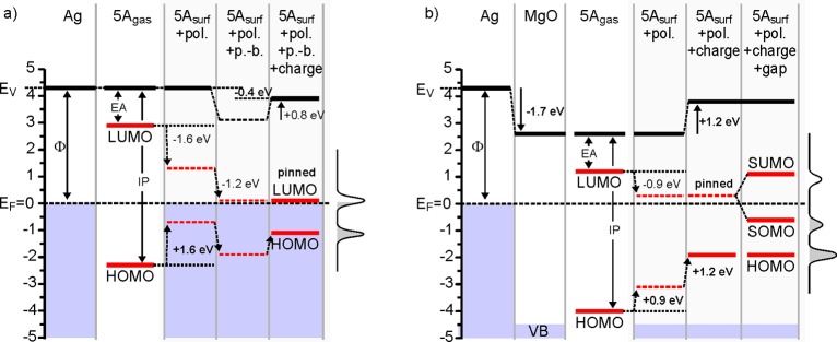
With the entire set of experimental results, we can now draw a picture of the energy level alignment, including an attempt to partition the various factors that influence the alignment and lead to the LUMO being close to EF, which is the necessary condition for the observed charge transfer (Figure 7). Naturally, these factors (polarizability, push-back, charge-transfer) are interconnected, and a partitioning is perhaps strictly not possible. However, intuitively, one can imagine that during the approach of the molecule to the surface, the major contributions to getting the LUMO to a point where charge transfer can occur come from HOMO–LUMO gap reduction due to the substrate polarizability and downward level-shifts because of push-back, while the final level alignment is affected by the charge-transfer dipole. It should be mentioned that as the molecule gets charged, additional contributions such as dynamic polarizability effects might influence the level alignment49 and lead to possible asymmetry in the gap reduction. These latter contributions cannot be estimated from our experimental data and are thus not taken into account here. However, an analysis of the effect of substrate polarizability based on DFT and using an approach similar to that given in ref (50) shows that our experimental estimates of the gap reduction due to substrate polarizability are reasonable (see Supporting Information).
Figure 7.
Partitioning of the energy level alignment for (a) 5A/Ag(001) and b) 5A/MgO(001)/Ag(001). The orbital energy levels (LUMO, HOMO) of isolated pentacene (5Agas) are aligned to the vacuum levels (EV) of Ag(001) and MgO(001)/Ag(001), and the contributions of polarization (pol.), push-back (p.-b.), charging (charge), and gap opening (gap, in b only) to the level alignment are added. The curves on the right side of each figure represent the measured spectra. Thick lines and bold numbers indicate experimentally determined energy levels and energy level shifts, whereas broken lines and normal numbers are derived level energies and shifts.
For 5A/Ag(001) (Figure 7a), we start by aligning the HOMO and LUMO levels with respect to the vacuum level (EV) of the system using the experimentally determined ionization potential (IP = 6.6 eV) and electron affinity (EA = 1.4 eV) of gas-phase 5A. As already mentioned, at the surface the polarizability of the environment will decrease the HOMO–LUMO gap. The decrease of the IP can be empirically estimated by taking the difference of the IPs of the 5A HOMO in the gas phase (IP5A,gas = 6.6 eV) and on the Ag(001) surface (IP5A/Ag(001) = Φ5A/Ag(001) + EB,HOMO = 5.0 eV), which is 1.6 eV. Since for the EA an increase of similar magnitude can be expected, the HOMO–LUMO gap is significantly reduced, and the LUMO level is pushed down, closer to EF.41,51 However, without a reduction of the WF (vacuum level), the EA is nevertheless not large enough to facilitate charge transfer. From WF measurements we know that the adsorption of 5A reduces the WF by 0.4 eV, which can be understood to result from push-back partly compensated by charge transfer. Since push-back reduces the WF, we estimate its effect to give rise to a 1.2 eV downward shift of all molecular levels, which brings the LUMO close to EF. As a result, charge transfer between Ag(001) and 5A is facilitated, and, while the partially occupied LUMO stays pinned at EF, the interface dipole created by the charged molecules increases the WF and shifts the HOMO level up. Note that in our analysis of the energy level alignment for the 5A/Ag(001) system, the different contributions of push-back and charge transfer can only indirectly be estimated with the help of the necessary requirement that the LUMO level has to be close to EF to enable charge transfer. In contrast, a similar analysis of the energy level alignment for the 5A/MgO(001)/Ag(001) system does not require any assumptions because the effects of push-back and charge transfer are separated.
For 5A/MgO(001)/Ag(001) (Figure 7b), we again start with the bare Ag(001) surface and the measured WF, which sets the vacuum level (EV) to 4.3 eV above EF. The formation of the MgO thin film reduces EV to 2.6 eV – a 1.7 eV reduction due to the push-back. As in the case of 5A/Ag(001), we align the HOMO and LUMO levels of gas-phase 5A with respect to the EV of the system and include the effect of the polarizability (determined in the same way as for 5A/Ag(001), using the WF and the energy of the HOMO level of 5A on MgO(001)/Ag(001)), which is naturally smaller than for 5A on Ag(001). This brings the LUMO very close to EF, enabling charge transfer from the substrate into the molecule. While the LUMO stays pinned at EF, the interface dipole created by the charging of the molecule leads to an increase of the WF by 1.2 eV and a corresponding shift of the HOMO level by the same magnitude. Because charge transfer through the dielectric barrier occurs by tunneling, the LUMO is occupied by an integer amount of charge, and the resulting singly occupied LUMO is split into a SOMO and a SUMO state separated by a gap of 1.7 eV, as determined by STS.
It is important to note that our experimental approach allows us to estimate separately the major factors that contribute to the energy level alignment as the molecule interacts with the surface. The consistency of this approach becomes immediately clear when comparing the experimentally measured level energies with those obtained by adding the various contributions of polarizability, push-back, and charge transfer to the vacuum level-aligned level energies of gas-phase 5A, as done in Figure 7, which are in perfect agreement with each other.
Conclusion
In conclusion, our study of the adsorption of pentacene (5A) on Ag(001) and Ag(001)-supported MgO(001) thin films provides a clear and comprehensive understanding of charge transfer and energy level alignment at these model inorganic/organic interfaces at a molecular level. Using WF measurements, STM and photoemission imaging and spectroscopy, together with DFT calculations, we show that the molecular LUMO gets pinned to the Fermi level on both substrates, and we are able to determine the individual contributions that affect the energy level alignment and lead to charging of the 5A molecule. In particular, the use of MgO(001) as thin dielectric layer enables us to demonstrate the transition from fractional charge transfer at the metal–organic interface to integer charge occupation of the molecular LUMO on an electronically decoupling, low-WF substrate. Our study unambiguously identifies the SOMO and SUMO of the singly charged pentacene anion adsorbed on the thin dielectric MgO layer and introduces an approach that permits the quantitative determination of the frontier orbital occupation.
In addition to addressing the problem of energy level alignment from a very fundamental point of view, our results are significant for the applied field, such as the organic device community. Dielectric interlayers are often used to improve charge injection at contacts.12 While they undoubtedly can reduce the electron injection barrier by WF reduction, if, as is the case here, the reduction is too great, integer charge transfer occurs and a significant gap opens, which renders their use counterproductive.
Methods
MgO(100) thin films were grown on clean Ag(001) surfaces following a recipe by J. Pal et al.52 The Ag(001) single crystal was cleaned by cycles of Ar+ sputtering (1 kV) and successive annealing (773 K, 2 min). Mg was deposited in an oxygen background of 1 × 10⁻⁶ mbar at a rate of 0.5 ML/min. During deposition, the Ag(001) crystal was kept at 573 K. The quality of the MgO thin film was checked by LEED and STM/STS. Pentacene was deposited at a sample temperature of Tsample = 300 K. The deposition rates were monitored with a quartz microbalance. STM and STS measurements were performed at 77 K with a Createc low-temperature STM attached to a ultrahigh-vacuum preparation chamber (base pressure 2 × 10⁻¹⁰ mbar) using electrochemically etched tungsten tips. The bias was applied to the sample, and during scanning on 5A covered surfaces, the tips were never intentionally functionalized. Angle-resolved photoemission spectroscopy (ARPES) measurements were performed using a goniometer-mounted VG ADES 400 spectrometer equipped with a helium gas discharge lamp (helium I, hν = 21.2 eV, angle of incidence α = 60°). Work functions were obtained from the secondary electron cutoff in normal emission with a sample bias. Photoemission tomography measurements were performed at the synchrotron radiation facility BESSY II (U125-2NIM beamline, hν = 21 eV, α = 40°) with a toroidal analyzer.53 The analyzer collects the full hemicircle of emission in the plane of incidence, and the momentum maps were obtained by rotating the crystal azimuth in 1° steps. Photoemission measurements reported in this work were taken at room temperature or 90 K.
DFT calculations were performed for the isolated 5A molecule by utilizing NWChem30 and for the full 5A/MgO(001)/Ag(001) and 5A/Ag(001) overlayers, for which the VASP code28,29 has been used. The calculations of the isolated molecule were performed using an OT-RSH functional.36 The simulated momentum maps of the HOMO and the LUMO of the isolated 5A molecule are obtained as Fourier transforms of the respective Kohn–Sham orbital as described in ref (43). The electronic structure calculations for 5A monolayers adsorbed on Ag(001) and MgO(001)/Ag(001) have been carried out using a repeated slab approach. The metallic substrate has been modeled by five metallic layers and the dielectric interface by two layers, and a vacuum layer of 15 Å has been added between the slabs. To avoid spurious electrical fields, a dipole layer is inserted in the vacuum region.54 Exchange–correlation effects were treated either within the GGA55 or within the HSE hybrid functional35 with k-point meshes of 4 × 8 × 1 and 2 × 4 × 1, respectively. The projector augmented wave (PAW)56 approach was used allowing for a relatively low kinetic energy cutoff of 500 eV, and a first-order Methfessel–Paxton smearing of 0.1 eV.57 During the geometry optimization, the atomic positions of the molecular layer, the dielectric interlayer, and the first two metallic layers were allowed to relax. In order to account for van der Waals interactions, we employ the vdW-surf method according to Ruiz et al.58,59 during the geometry optimization.
Acknowledgments
We thank the Helmholtz-Zentrum Berlin-Electron storage ring BESSY II for provision of synchrotron radiation at beamline U125/2-NIM and Xiaosheng Yang for help during the beamtime. Financial support from Austrian Science Fund (FWF): P21330-N20, P27649-N20, P27427 is gratefully acknowledged. The computational results presented have been achieved using the computing facilities of the University of Graz and the Vienna Scientific Cluster (VSC3).
Supporting Information Available
The Supporting Information is available free of charge on the ACS Publications website at DOI: 10.1021/acsnano.7b02449.
Theoretical estimation of the contribution of static substrate polarizability on HOMO–LUMO gap reduction (PDF)
The authors declare no competing financial interest.
Supplementary Material
References
- Oxide Ultrathin Films: Science and Technology; Pacchioni G., Valeri S., Eds.; Wiley-VCH: Weinheim, 2011. [Google Scholar]
- Oxide Materials at the Two-Dimensional Limit, Springer Series in Materials Science; Netzer F. P., Fortunelli A., Eds.; Springer International Publishing: Switzerland, 2016; Vol. 234. [Google Scholar]
- Repp J.; Meyer G.; Stojkovic S. M.; Gourdon A.; Joachim C. Molecules on Insulating Films: Scanning-Tunneling Microscopy Imaging of Individual Molecular Orbitals. Phys. Rev. Lett. 2005, 94, 026803. 10.1103/PhysRevLett.94.026803. [DOI] [PubMed] [Google Scholar]
- Swart I.; Sonnleitner T.; Repp J. Charge State Control of Molecules Reveals Modification of the Tunneling Barrier with Intramolecular Contrast. Nano Lett. 2011, 11, 1580–1584. 10.1021/nl104452x. [DOI] [PubMed] [Google Scholar]
- Repp J.; Meyer G.; Olsson F. E.; Persson M. Controlling the Charge State of Individual Gold Adatoms. Science 2004, 305, 493–495. 10.1126/science.1099557. [DOI] [PubMed] [Google Scholar]
- Rau I. G.; Baumann S.; Rusponi S.; Donati F.; Stepanow S.; Gragnaniello L.; Dreiser J.; Piamonteze C.; Nolting F.; Gangopadhyay S.; Albertini O. R.; Macfarlane R. M.; Lutz C. P.; Jones B. A.; Gambardella P.; Heinrich A. J.; Brune H. Reaching the Magnetic Anisotropy Limit of a 3d Metal Atom. Science 2014, 344, 988–992. 10.1126/science.1252841. [DOI] [PubMed] [Google Scholar]
- Pacchioni G.; Giordano L.; Baistrocchi M. Charging of Metal Atoms on Ultrathin MgO/Mo(100) Films. Phys. Rev. Lett. 2005, 94, 226104. 10.1103/PhysRevLett.94.226104. [DOI] [PubMed] [Google Scholar]
- Sterrer M.; Risse T.; Pozzoni U. M.; Giordano L.; Heyde M.; Rust H. P.; Pacchioni G.; Freund H.-J. Control of the Charge State of Metal Atoms on Thin MgO Films. Phys. Rev. Lett. 2007, 98, 096107. 10.1103/PhysRevLett.98.096107. [DOI] [PubMed] [Google Scholar]
- Sun Y. N.; Qin Z. H.; Lewandowski M.; Carrasco E.; Sterrer M.; Shaikhutdinov S.; Freund H. J. Monolayer Iron Oxide Film on Platinum Promotes Low Temperature CO Oxidation. J. Catal. 2009, 266, 359–368. 10.1016/j.jcat.2009.07.002. [DOI] [Google Scholar]
- Sun Y. N.; Giordano L.; Goniakowski J.; Lewandowski M.; Qin Z. H.; Noguera C.; Shaikhutdinov S.; Pacchioni G.; Freund H. J. The Interplay between Structure and CO Oxidation Catalysis on Metal-Supported Ultrathin Oxide Films. Angew. Chem., Int. Ed. 2010, 49, 4418–4421. 10.1002/anie.201000437. [DOI] [PubMed] [Google Scholar]
- Calaza F.; Stiehler C.; Fujimori Y.; Sterrer M.; Beeg S.; Ruiz-Oses M.; Nilius N.; Heyde M.; Parviainen T.; Honkala K.; Häkkinen H.; Freund H. J. Carbon Dioxide Activation and Reaction Induced by Electron Transfer at an Oxide-Metal Interface. Angew. Chem., Int. Ed. 2015, 54, 12484–12487. 10.1002/anie.201501420. [DOI] [PubMed] [Google Scholar]
- Greiner M. T.; Helander M. G.; Tang W. M.; Wang Z. B.; Qiu J.; Lu Z. H. Universal Energy-Level Alignment of Molecules on Metal Oxides. Nat. Mater. 2012, 11, 76–81. 10.1038/nmat3159. [DOI] [PubMed] [Google Scholar]
- Jönsson S. K. M.; Salaneck W. R.; Fahlman M. Photoemission of AlQ(3) and C-60 Films on Al and LiF/Al Substrates. J. Appl. Phys. 2005, 98, 014901. 10.1063/1.1929884. [DOI] [Google Scholar]
- Hofmann O. T.; Rinke P.; Scheffler M.; Heimel G. Integer versus Fractional Charge Transfer at Metal(/Insulator)/Organic Interfaces: Cu(/NaCl)/TCNE. ACS Nano 2015, 9, 5391–5404. 10.1021/acsnano.5b01164. [DOI] [PMC free article] [PubMed] [Google Scholar]
- Gruenewald M.; Schirra L. K.; Winget P.; Kozlik M.; Ndione P. F.; Sigdel A. K.; Berry J. J.; Forker R.; Bredas J. L.; Fritz T.; Monti O. L. A. Integer Charge Transfer and Hybridization at an Organic Semiconductor/Conductive Oxide Interface. J. Phys. Chem. C 2015, 119, 4865–4873. 10.1021/jp512153b. [DOI] [Google Scholar]
- Mohn F.; Repp J.; Gross L.; Meyer G.; Dyer M. S.; Persson M. Reversible Bond Formation in a Gold-Atom-Organic-Molecule Complex as a Molecular Switch. Phys. Rev. Lett. 2010, 105, 266102. 10.1103/PhysRevLett.105.266102. [DOI] [PubMed] [Google Scholar]
- Amsalem P.; Niederhausen J.; Wilke A.; Heimel G.; Schlesinger R.; Winkler S.; Vollmer A.; Rabe J. P.; Koch N. Role of Charge Transfer, Dipole-Dipole Interactions, and Electrostatics in Fermi-Level Pinning at a Molecular Heterojunction on a Metal Surface. Phys. Rev. B: Condens. Matter Mater. Phys. 2013, 87, 035440. 10.1103/PhysRevB.87.035440. [DOI] [Google Scholar]
- Witte G.; Lukas S.; Bagus P. S.; Wöll C. Vacuum Level Alignment at Organic/Metal Junctions: ″Cushion″ Effect and the Interface Dipole. Appl. Phys. Lett. 2005, 87, 263502. 10.1063/1.2151253. [DOI] [Google Scholar]
- Willenbockel M.; Lüftner D.; Stadtmüller B.; Koller G.; Kumpf C.; Soubatch S.; Puschnig P.; Ramsey M. G.; Tautz F. S. The Interplay Between Interface Structure, Energy Level Alignment and Chemical Bonding Strength at Organic-Metal Interfaces. Phys. Chem. Chem. Phys. 2015, 17, 1530–1548. 10.1039/C4CP04595E. [DOI] [PubMed] [Google Scholar]
- Gross L.; Moll N.; Mohn F.; Curioni A.; Meyer G.; Hanke F.; Persson M. High-Resolution Molecular Orbital Imaging Using a p-Wave STM Tip. Phys. Rev. Lett. 2011, 107, 086101. 10.1103/PhysRevLett.107.086101. [DOI] [PubMed] [Google Scholar]
- Gross L.; Mohn F.; Moll N.; Liljeroth P.; Meyer G. The Chemical Structure of a Molecule Resolved by Atomic Force Microscopy. Science 2009, 325, 1110–1114. 10.1126/science.1176210. [DOI] [PubMed] [Google Scholar]
- Soe W. H.; Manzano C.; De Sarkar A.; Chandrasekhar N.; Joachim C. Direct Observation of Molecular Orbitals of Pentacene Physisorbed on Au(111) by Scanning Tunneling Microscope. Phys. Rev. Lett. 2009, 102, 176102. 10.1103/PhysRevLett.102.176102. [DOI] [PubMed] [Google Scholar]
- Jaouen T.; Jezequel G.; Delhaye G.; Lepine B.; Turban P.; Schieffer P. Work Function Shifts, Schottky Barrier Height, and Ionization Potential Determination of Thin MgO Films on Ag(001). Appl. Phys. Lett. 2010, 97, 232104. 10.1063/1.3525159. [DOI] [Google Scholar]
- König T.; Simon G. H.; Rust H. P.; Heyde M. Work Function Measurements of Thin Oxide Films on Metals-MgO on Ag(001). J. Phys. Chem. C 2009, 113, 11301–11305. 10.1021/jp901226q. [DOI] [Google Scholar]
- Giordano L.; Cinquini F.; Pacchioni G. Tuning the Surface Metal Work Function by Deposition of Ultrathin Oxide Films: Density Functional Calculations. Phys. Rev. B: Condens. Matter Mater. Phys. 2006, 73, 045414. 10.1103/PhysRevB.73.045414. [DOI] [Google Scholar]
- Braun S.; Salaneck W. R.; Fahlman M. Energy-Level Alignment at Organic/Metal and Organic/Organic Interfaces. Adv. Mater. 2009, 21, 1450–1472. 10.1002/adma.200802893. [DOI] [Google Scholar]
- Repp J.; Meyer G.; Paavilainen S.; Olsson F. E.; Persson M. Imaging Bond Formation Between a Gold Atom and Pentacene on an Insulating Surface. Science 2006, 312, 1196–1199. 10.1126/science.1126073. [DOI] [PubMed] [Google Scholar]
- Kresse G.; Hafner J. Ab-initio Molecular Dynamics for Liquid Metals. Phys. Rev. B: Condens. Matter Mater. Phys. 1993, 47, 558–561. 10.1103/PhysRevB.47.558. [DOI] [PubMed] [Google Scholar]
- Kresse G.; Joubert D. From Ultrasoft Pseudopotentials to the Projector Augmented-Wave Method. Phys. Rev. B: Condens. Matter Mater. Phys. 1999, 59, 1758–1775. 10.1103/PhysRevB.59.1758. [DOI] [Google Scholar]
- Valiev M.; Bylaska E. J.; Govind N.; Kowalski K.; Straatsma T. P.; Van Dam H. J. J.; Wang D.; Nieplocha J.; Apra E.; Windus T. L.; de Jong W. NWChem: A Comprehensive and Scalable Open-Source Solution for Large Scale Molecular Simulations. Comput. Phys. Commun. 2010, 181, 1477–1489. 10.1016/j.cpc.2010.04.018. [DOI] [Google Scholar]
- Ules T.; Lüftner D.; Reinisch E. M.; Koller G.; Puschnig P.; Ramsey M. G. Orbital Tomography of Hybridized and Dispersing Molecular Overlayers. Phys. Rev. B: Condens. Matter Mater. Phys. 2014, 90, 155430. 10.1103/PhysRevB.90.155430. [DOI] [Google Scholar]
- Romaner L.; Nabok D.; Puschnig P.; Zojer E.; Ambrosch-Draxl C. Theoretical Study of PTCDA Adsorbed on the Coinage Metal Surfaces, Ag(111), Au(111) and Cu(111). New J. Phys. 2009, 11, 053010. 10.1088/1367-2630/11/5/053010. [DOI] [Google Scholar]
- Honkala K.; Häkkinen H. Au Adsorption on Regular and Defected Thin MgO(100) Films Supported by Mo. J. Phys. Chem. C 2007, 111, 4319–4327. 10.1021/jp066822l. [DOI] [Google Scholar]
- Giordano L.; Martinez U.; Sicolo S.; Pacchioni G. Observable Consequences of Formation of Au Anions from Deposition of Au Atoms on Ultrathin Oxide Films. J. Chem. Phys. 2007, 127, 144713. 10.1063/1.2794339. [DOI] [PubMed] [Google Scholar]
- Heyd J.; Scuseria G. E.; Ernzerhof M. Hybrid Functionals Based on a Screened Coulomb Potential (vol 118, pg 8207, 2003). J. Chem. Phys. 2006, 124, 219906. 10.1063/1.2204597. [DOI] [Google Scholar]
- Kronik L.; Stein T.; Refaely-Abramson S.; Baer R. Excitation Gaps of Finite-Sized Systems from Optimally Tuned Range-Separated Hybrid Functionals. J. Chem. Theory Comput. 2012, 8, 1515–1531. 10.1021/ct2009363. [DOI] [PubMed] [Google Scholar]
- Refaely-Abramson S.; Baer R.; Kronik L. Fundamental and Excitation Gaps in Molecules of Relevance for Organic Photovoltaics from an Optimally Tuned Range-Separated Hybrid Functional. Phys. Rev. B: Condens. Matter Mater. Phys. 2011, 84, 075144. 10.1103/PhysRevB.84.075144. [DOI] [Google Scholar]
- Refaely-Abramson S.; Sharifzadeh S.; Govind N.; Autschbach J.; Neaton J. B.; Baer R.; Kronik L. Quasiparticle Spectra from a Nonempirical Optimally Tuned Range-Separated Hybrid Density Functional. Phys. Rev. Lett. 2012, 109, 226405. 10.1103/PhysRevLett.109.226405. [DOI] [PubMed] [Google Scholar]
- Refaely-Abramson S.; Sharifzadeh S.; Jain M.; Baer R.; Neaton J. B.; Kronik L. Gap Renormalization of Molecular Crystals from Density Functional Theory. Phys. Rev. B: Condens. Matter Mater. Phys. 2013, 88, 081204. 10.1103/PhysRevB.88.081204. [DOI] [Google Scholar]
- Lüftner D.; Milko M.; Huppmann S.; Scholz M.; Ngyuen N.; Wiessner M.; Scholl A.; Reinert F.; Puschnig P. CuPc/Au(110): Determination of the Azimuthal Alignment by a Combination of Angle-Resolved Photoemission and Density Functional Theory. J. Electron Spectrosc. Relat. Phenom. 2014, 195, 293–300. 10.1016/j.elspec.2014.06.002. [DOI] [PMC free article] [PubMed] [Google Scholar]
- Liu Z.-F.; Egger D. A.; Refaely-Abramson S.; Kronik L.; Neaton J. B. Energy Level Alignment at Molecule-Metal Interfaces from an Optimally Tuned Range-Separated Hybrid Functional. J. Chem. Phys. 2017, 146, 092326. 10.1063/1.4975321. [DOI] [Google Scholar]
- Egger D. A.; Liu Z. F.; Neaton J. B.; Kronik L. Reliable Energy Level Alignment at Physisorbed Molecule-Metal Interfaces from Density Functional Theory. Nano Lett. 2015, 15, 2448–2455. 10.1021/nl504863r. [DOI] [PMC free article] [PubMed] [Google Scholar]
- Puschnig P.; Berkebile S.; Fleming A. J.; Koller G.; Emtsev K.; Seyller T.; Riley J. D.; Ambrosch-Draxl C.; Netzer F. P.; Ramsey M. G. Reconstruction of Molecular Orbital Densities from Photoemission Data. Science 2009, 326, 702–706. 10.1126/science.1176105. [DOI] [PubMed] [Google Scholar]
- Ules T.; Lüftner D.; Reinisch E. M.; Koller G.; Puschnig P.; Ramsey M. G. Continuous or Discrete: Tuning the Energy Level Alignment of Organic Layers with Alkali Dopants. Phys. Rev. B: Condens. Matter Mater. Phys. 2016, 94, 205405. 10.1103/PhysRevB.94.205405. [DOI] [Google Scholar]
- Wiessner M.; Hauschild D.; Sauer C.; Feyer V.; Scholl A.; Reinert F. Complete Determination of Molecular Orbitals by Measurement of Phase Symmetry and Electron Density. Nat. Commun. 2014, 5, 4156. 10.1038/ncomms5156. [DOI] [PubMed] [Google Scholar]
- Weiß S.; Lüftner D.; Ules T.; Reinisch E. M.; Kaser H.; Gottwald A.; Richter M.; Soubatch S.; Koller G.; Ramsey M. G.; Tautz F. S.; Puschnig P. Exploring Three-Dimensional Orbital Imaging with Energy-Dependent Photoemission Tomography. Nat. Commun. 2015, 6, 8287. 10.1038/ncomms9287. [DOI] [PMC free article] [PubMed] [Google Scholar]
- Wang H.; Amsalem P.; Heimel G.; Salzmann I.; Koch N.; Oehzelt M. Band-Bending in Organic Semiconductors: The Role of Alkali-Halide Interlayers. Adv. Mater. 2014, 26, 925–930. 10.1002/adma.201303467. [DOI] [PubMed] [Google Scholar]
- Wu S. W.; Nazin G. V.; Chen X.; Qiu X. H.; Ho W. Control of Relative Tunneling Rates in Single Molecule Bipolar Electron Transport. Phys. Rev. Lett. 2004, 93, 236802. 10.1103/PhysRevLett.93.236802. [DOI] [PubMed] [Google Scholar]
- Sau J. D.; Neaton J. B.; Choi H. J.; Louie S. G.; Cohen M. L. Electronic Energy Levels of Weakly Coupled Nanostructures: C60-Metal Interfaces. Phys. Rev. Lett. 2008, 101, 026804. 10.1103/PhysRevLett.101.026804. [DOI] [PubMed] [Google Scholar]
- Khoo K. H.; Chen Y.; Li S.; Quek S. Y. Length Dependence of Electron Transport Through Molecular Wires – A First Principles Perspective. Phys. Chem. Chem. Phys. 2015, 17, 77–96. 10.1039/C4CP05006A. [DOI] [PubMed] [Google Scholar]
- Neaton J. B.; Hybertsen M. S.; Louie S. G. Renormalization of Molecular Electronic Levels at Metal-Molecule Interfaces. Phys. Rev. Lett. 2006, 97, 216405. 10.1103/PhysRevLett.97.216405. [DOI] [PubMed] [Google Scholar]
- Pal J.; Smerieri M.; Celasco E.; Savio L.; Vattuone L.; Rocca M. Morphology of Monolayer MgO Films on Ag(100): Switching from Corrugated Islands to Extended Flat Terraces. Phys. Rev. Lett. 2014, 112, 126102. 10.1103/PhysRevLett.112.126102. [DOI] [PubMed] [Google Scholar]
- Broekman L.; Tadich A.; Huwald E.; Riley J.; Leckey R.; Seyller T.; Emtsev K.; Ley L. First Results from a Second Generation Toroidal Electron Spectrometer. J. Electron Spectrosc. Relat. Phenom. 2005, 144-147, 1001–1004. 10.1016/j.elspec.2005.01.022. [DOI] [Google Scholar]
- Neugebauer J.; Scheffler M. Adsorbate-Substrate and Adsorbate-Adsorbate Interactions of Na and K Adlayers on Al(111). Phys. Rev. B: Condens. Matter Mater. Phys. 1992, 46, 16067–16080. 10.1103/PhysRevB.46.16067. [DOI] [PubMed] [Google Scholar]
- Perdew J. P.; Burke K.; Ernzerhof M. Generalized Gradient Approximation Made Simple. Phys. Rev. Lett. 1996, 77, 3865–3868. 10.1103/PhysRevLett.77.3865. [DOI] [PubMed] [Google Scholar]
- Blöchl P. E. Projector Augmented-Wave Method. Phys. Rev. B: Condens. Matter Mater. Phys. 1994, 50, 17953–17979. 10.1103/PhysRevB.50.17953. [DOI] [PubMed] [Google Scholar]
- Methfessel M.; Paxton A. T. High-Precision Sampling for Brillouin-Zone Integration in Metals. Phys. Rev. B: Condens. Matter Mater. Phys. 1989, 40, 3616–3621. 10.1103/PhysRevB.40.3616. [DOI] [PubMed] [Google Scholar]
- Tkatchenko A.; Scheffler M. Accurate Molecular van der Waals Interactions from Ground-State Electron Density and Free-Atom Reference Data. Phys. Rev. Lett. 2009, 102, 073005. 10.1103/PhysRevLett.102.073005. [DOI] [PubMed] [Google Scholar]
- Ruiz V. G.; Liu W.; Zojer E.; Scheffler M.; Tkatchenko A. Density-Functional Theory with Screened van der Waals Interactions for the Modeling of Hybrid Inorganic-Organic Systems. Phys. Rev. Lett. 2012, 108, 146103. 10.1103/PhysRevLett.108.146103. [DOI] [PubMed] [Google Scholar]
Associated Data
This section collects any data citations, data availability statements, or supplementary materials included in this article.


