Abstract
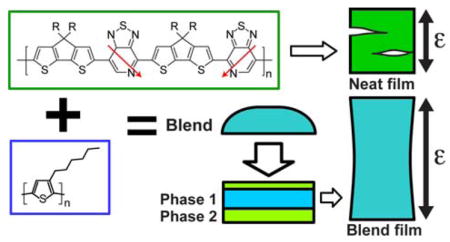
Polymer semiconductors based on donor-acceptor monomers have recently resulted in significant gains in field effect mobility in organic thin film transistors (OTFTs). These polymers incorporate fused aromatic rings and have been designed to have stiff planar backbones, resulting in strong intermolecular interactions, which subsequently result in stiff and brittle films. The complex synthesis typically required for these materials may also result in increased production costs. Thus, developing methods to improve mechanical plasticity while lowering material consumption during fabrication will significantly improve opportunities for adoption in flexible and stretchable electronics. To achieve these goals, we consider blending a brittle donor-acceptor polymer poly[4-(4,4-dihexadecyl-4H-cyclopenta[1,2-b:5,4-b′]dithiopen-2-yl)-alt-[1,2,5]thiadiazolo[3,4-c]pyridine] (PCDTPT) with ductile poly(3-hexylthiophene). We find that the ductility of the blend film is significantly improved compared to neat PCDTPT films, and when employed in an OTFT, the performance is largely maintained. The ability to maintain charge transport character is due to vertical segregation within the blend, while the improved ductility is achieved due to intermixing of the polymers throughout the film thickness. Importantly, applying large strains to the ductile films is shown to orient both polymers, which further increases charge carrier mobility. These results highlight a processing approach to achieve high performance polymer OTFTs that are electrically and mechanically optimized.
Keywords: polymer semiconductors, blend films, vertical segregation, ductility, thin film transistors
Graphical Abstract
1. Introduction
Multi-component polymer films cast from a common solution where one constituent material is a semiconductor and a second is an insulating commodity polymer has a number of potential advantages for the development of organic thin film transistors (OTFTs).1–12 The blend solution provides an opportunity to encapsulate the environmentally sensitive active layer,4 reduce the use of the costly semiconductor material, and manage solution viscosity for processing optimization.2,10,12 There are also potential mechanical benefits where blending an appropriate secondary polymer can improve the ductility and strength of the film. For example, demonstrations include blending high density polyethylene (PE) with doped polythiophene, where the ductility of bulk samples increased significantly while electrical conduction through the sample was still possible.13 The use of block-copolymers composed of poly(3-hexylthiophene) (P3HT) and PE was also shown to increase film ductility and strength while the performance of these films, in their unstrained state, were similar to neat polythiophene films for both bulk charge transport measured in a diode configuration, and in-plane charge transport measured in an OTFT.14 In a recent report, P3HT fibrils were embedded into an elastomer host resulting in highly stretchable composite, although with a drop in mobility compared to the fibril network in an unstrained state.15
In demonstrations of polymer semiconductor blend films used in OTFTs, the polymer semiconductors employed have largely been polythiophenes: poly(3-hexylthiophene) (P3HT), poly(2,5-bis(3-dodecylthiophene-2-yl)thieno[3,2-b]thiophene) (pBTTT), and poly[5,5′-bis(3-dodecyl-2-thienyl)-2,2′-bithiophene (PQT).2,5,7,9,10,16 Here, we are interested in employing the blend film approach to high performance donor-acceptor polymers with a focus on increasing film ductility while maintaining OTFT performance. Polymer semiconductors based on donor-acceptor monomers have garnered considerable attention for application in OTFTs due to their significant gains in field effect mobility.17,18 The high charge mobility in this class of materials is associated with highly planar polymer backbones, and strong intramolecular interactions that improve local polymer order and increase charge delocalization.17,18 This results in polymers with rigid backbones and strong intermolecular interactions that can lead to films that fracture at a few percent strain.19 Here, we show that blending the donor-acceptor polymer with a secondary ductile polymer significantly increases the film ductility. The polymer blend films have performance associated with the higher performance polymer while increasing the film ductility such that when strain is applied to the film, the polymer backbones align in the direction of strain and the charge mobility in the chain alignment direction increases compared to an unstrained film. The increase in ductility is key to realizing physically robust flexible and stretchable devices.15,17–19, In particular, retaining similar performance under large strains is a powerful screening tool to asses the suitability of a material for stretchable device applications.20,21 These results highlight a design approach capable of achieving high mobility and highly ductile polymer semiconductor films.
In this work, we consider the donor-acceptor polymer poly[4-(4,4-dihexadecyl-4H-cyclopenta[1,2-b:5,4-b′]dithiophen-2-yl)-alt-[1,2,5]thiadiazolo[3,4-c]pyridine] (PCDTPT) with molecular structure given in Figure 1.22,23 The crack onset strain of PCDTPT occurs at ≤ 4 % strain as determined by straining the film on an elastomer host substrate and observing the film under optical microscopy. A neat PCDTPT film strained by 10 % is pictured in Figure 1 showing clear tearing in the film. A strain larger than crack-onset is imaged to highlight the tearing in the film. To improve ductility we blend this polymer with P3HT. The use of the polymer semiconductor P3HT as the secondary material is a departure from previous studies where the secondary material has typically been an insulating polymer. P3HT was chosen as the secondary polymer for several reasons. The high molecular weight P3HT used in this study is known to be ductile at room temperature with a glass transition temperature below room temperature.24,25 P3HT is semicrystalline with strong aggregation characteristics that will promote segregation of the polymers. P3HT is a well characterized system such that variations in morphology can be probed optically and with diffraction.26,27 In addition, the absorption spectrum of P3HT does not significantly overlap with the absorption spectrum of PCDTPT, allowing the components to be characterized by UV-visible optical spectroscopy. We show that blending P3HT with PCDTPT can significantly increase film ductility while largely maintaining the charge transport characteristics in an OTFT configuration. Furthermore, the increased ductility allows for large strains to be applied to the film orienting the polymers in the plane of the film, resulting in an increase in charge mobility relative to the neat PCDTPT counterpart. Importantly, in blend films for OTFTs, it is typically desirable to promote vertical segregation within the film such that the semiconductor is found near the gate dielectric surface. This helps ensure that the narrow region of the film that is responsible for charge transport is composed of the desired semiconductor material. This then suggests that we require a blend film system that will increase ductility and have vertical segregation, potentially conflicting design requirements. The ability to achieve high ductility and mobility demonstrated here is attributed to a unique morphology that includes vertical segregation of the components while maintaining some intermixing of the polymers through the film thickness. Below, we first discuss the OTFT performance of the blend films followed by morphological characterization and analysis of film ductility.
Figure 1.
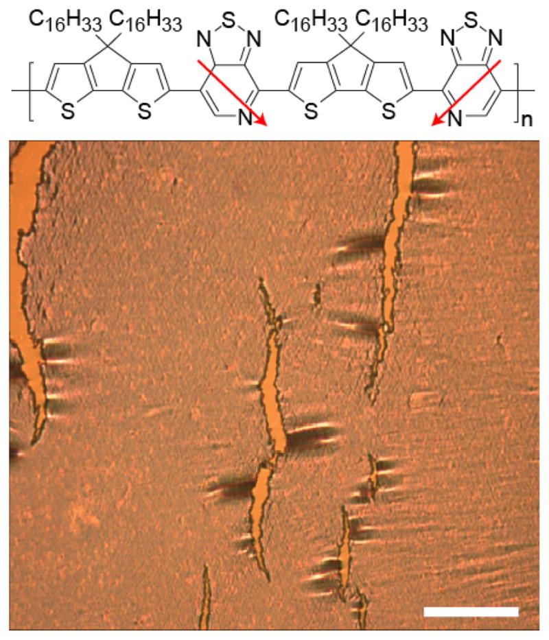
Optical microscope image of cracked PCDTPT at 10 % strain. The scale bar is 40 μm. Top, molecular structure of PCDTPT.
2. Results and Discussion
Processing Considerations and OTFT Performance
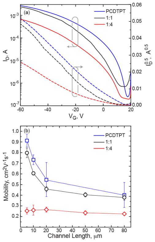
Blend films were cast from solutions composed of 1:0, 1:1, and 1:4 weight ratio of PCDTPT:P3HT dissolved in a 1:1 volume ratio of 1,2-dichlorobenzene:chloroform. The solutions were spun cast at room temperature onto octyltrichlorosilane (OTS) treated Si substrates. Charge transport characteristics were measured in a bottom-gate bottom-contact OTFT configuration with a focus on saturated field effect mobility. The transfer and output characteristics of 5 μm devices are given in Figure 2(a) and Figure S1, respectively. The channel length dependence of the saturated mobility is also shown in Figure 2(b). We find that the neat PCDTPT film has the highest saturated field effect mobility followed by the 1:1 blend film, where the mobility for 5 μm channel length devices were approximately 0.9 cm2V−1s−1 and 0.8 cm2V−1s−1, respectively. These films are also found to have a similar channel length behavior. Going to the 1:4 film, there is a drop in mobility and a flatter channel length dependence.
Figure 2.
(a) OTFT transfer curves for 5 μm devices for neat PCDTPT, 1:1 PCDTPT:P3HT, and 1:4 PCDTPT:P3HT blend films. (b) Channel length behavior of the saturated field effect mobility for these films.
To gain insight into this channel length behavior, contact resistance analysis was performed on each film type following a previously described process,28 with details provided in the supporting information and results giving in Figure S2. The 1:4 blend film is found to have a higher contact resistance compared to the other films, and all films have a similar channel resistance. In the 1:4 blend film the contact resistance is significantly higher than the channel resistance per μm of channel length, such that one would expect a significant influence on the measured mobility for the shorter channel length devices,29 which supports the flatter channel length dependence observed for these films. Nevertheless, the relatively high charge mobility in the both blend films suggests that PCDTPT is primarily responsible for charge transport. While there is a drop in mobility for the 1:4 film, PCDTPT is still believed to be the primary charge carrier material given that P3HT typically has an order of magnitude lower mobility.30 The charge transport characteristics suggest we have vertical segregation of the materials within the film, with PCDTPT preferentially segregating to the bottom interface.
Film Morphology
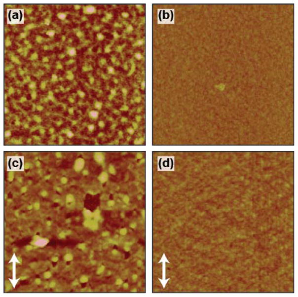
We begin the morphological characterization by investigating the segregation behavior of the polymers in the films. Segregation in polymer blends commonly occurs due to the low entropy gain upon mixing.3,31 This segregation can be both lateral and vertical in nature. Several factors can contribute to the vertical segregation within the film including the interaction energy between the film/substrate and film/air interfaces,3,32,33 crystallization order of the components,2 and solubility differences of the materials in the solution.7,12,31 In cast films, lateral segregation can also develop due to polymer interface instabilities during solidification.31 Lateral segregation is first considered by inspection by atomic force microscopy (AFM) and optical microscopy, with characteristic images shown in Figure 3 and Figure S3, respectively. We see that the 1:1 film has nanoscale nodules that can be attributed to lateral segregation of PCDTPT within the film. This is supported in part by the distinct color of the nodules observed in the microscope images. An AFM image of a neat PCDTPT film is also provided in Figure S4 where no signs of nodule formation are visible, showing that this formation is not inherent to the PCDTPT film. In the 1:4 blend, the film is relatively smooth without any signs of significant lateral segregation of the polymers.
Figure 3.
Atomic force microscope images of the spun cast (a) 1:1 and (b) 1:4 ratio PCDTPT:P3HT blend films. Images of 75 % strained (c) 1:1 and (d) 1:4 ratio PCDTPT:P3HT blend films. The applied strain direction is given in the bottom left corner of the strained films. All images are 10 μm by 10 μm.
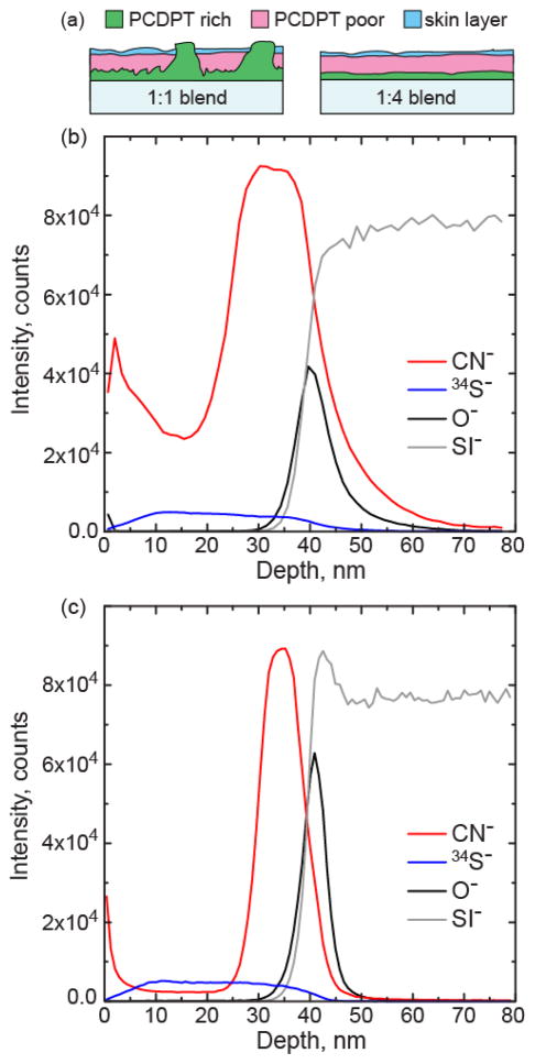
To determine the vertical segregation character, the blend films were measured with Time-of-Flight Secondary Ion Mass Spectrometry (TOF-SIMS). TOF SIMS depth profiles for the 1:1 and 1:4 films are shown in Figure 4(b,c). For the polymers under consideration, the nitrogen in the PCDTPT provides a unique marker for depth profiling through the CN− ion. Also shown in the SIMS depth profile is O− and Si−, which captures the Si substrate with its native oxide layer.
Figure 4.
(a) Schematic of the segregation character of the 1:1 and 1:4 blend films. (b,c) TOF-SIMS results for vertical segregation of the (b) 1:1 and (c) 1:4 blend film on a Si substrate with native oxide layer. The CN− ion is unique to the PCDTPT polymer.
From these depth profiles, segregation of the PCDTPT is clearly visible, and the blend films can be roughly divided into 3 regions. The bottom of the film is PCDTPT rich, the middle of the film has a significantly reduced PCDTPT concentration, and the top of the film we find that the PCDTPT begins to increase again in concentration, as illustrated in Figure 4(a). The relative fraction of the PCDTPT in the middle region of the film is greater in the 1:1 film compared to the 1:4 film, likely due to the lateral segregation of the PCDTPT resulting in pure aggregates that form through the film thickness. In addition, as the ratio of PCDTPT in the blend drops, the PCDTPT rich bottom layer becomes thinner. The depth resolution of the 1:1 film also appears to be poorer than the 1:4 film, which is most likely due to the rougher initial surface of the 1:1 film as a result of the lateral segregation. While clear vertical segregation is observed with TOF-SIMS, it does not provide information on the purity of the bottom PCDTPT rich region. To determine if both polymers are still found near the surface of the film, X-ray photoelectron spectroscopy (XPS) measurements are made on neat P3HT and PCDTPT films and 1:4 blend films, with data provided in Figure S5. Results show that the bottom surface of the blend film has signatures associated with both P3HT and PCDTPT. A characteristic N 1s peak is evident at 400 eV confirming the presence of PCDTPT at this interface while the C 1s peak at 286 eV and the S 2p peak at 164 eV indicate the presence of P3HT. Thus, while there is vertical segregation of the PCDTPT to the bottom surface of the film, a fraction of P3HT remains distributed near the surface. The fraction of P3HT at the surface is not quantitatively determined in this report. However, the TOF-SIMS is consistent with the OTFT measurements that suggest the surface in contact with the gate dielectric is composed primarily of PCDTPT.
Fully describing the phase separation of the polymers is out of the scope of this article. However, we provide here possible mechanisms that are driving the segregation behavior. The vertical segregation observed in the films is primarily attributed to preferential wetting of the PCDTPT to the film surfaces. The surface interactions are considered by measuring the contact angle of saturated PCDTPT and P3HT solutions in 1,2-dichlorobenzene on OTS-treated Si. The contact angles were determined to be 42° for PCDTPT and 52° for P3HT. These results suggest that PCDTPT preferentially wets the substrate surface.5 Preferential solubility of the polymers may also be a factor in the vertical segregation characteristics.5,7,12,34,35 During spin coating, a gradient in solvent concentration can form in the film where solvent evaporation from the top of the film is faster the solvent diffusion through the film.31 Thus, the polymer with lower solubility will be rejected from the solvent poor region of the film toward the more solvent rich region near the substrate surface. 4,5,12 We have not completed a full solubility analysis, but believe that the PCDTPT is not as soluble as P3HT in the co-solvent mixture. The high higher molecular weight of the PCDTPT and the stiff polymer backbone reduces its solubility as previously reported.22 Thus the PCDTPT may be driven toward the bottom surface during the casting process. Given that the TOF-SIMS data shows a PCDTPT rich region at both the air and substrate interfaces of the film, this mechanism is believed to be secondary to preferential wetting. The solvent gradient along with polymer-polymer interface interaction can also drive lateral segregation.31 The variation in polymer blend ratio along with the solidification rate and the solvent gradient during casting likely drives the differences observed in the lateral segregation in the films. The greater lateral segregation found in the 1:4 blend films may partially cause the lower mobility in these films compared to the 1:1 blend films.
Finally, it should be noted that the processing approach used here is a fast cast method processed at room temperature. This approach simplifies the casting procedure considerably compared to previous polymer blend OTFT approaches that required elevated temperature casting with fine control of solidification order and rate.2 Nor does the method use a marginal solvent approach to promote polymer segregation that requires careful solution design.7,34 The trade-off compared to these other methods is the limited ability to minimize the active polymer semiconductor in the blend film while still maintaining high OTFT performance.
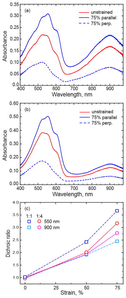
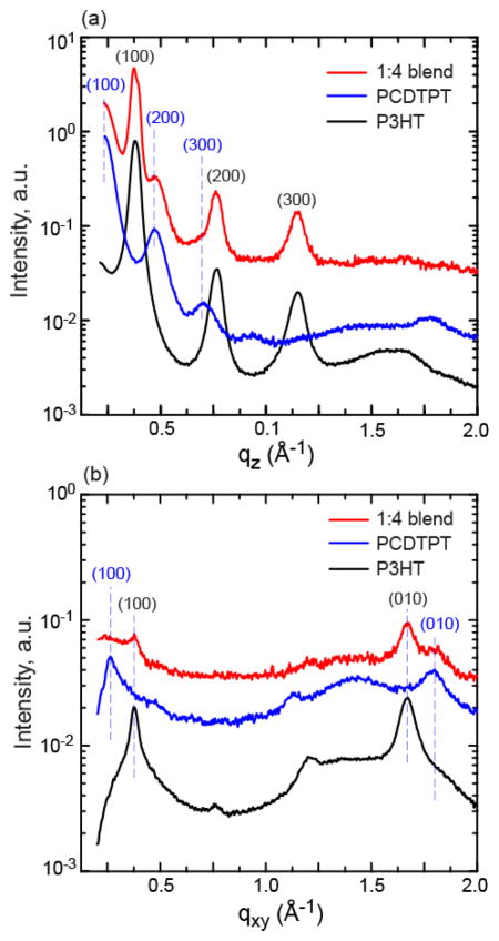
The segregation and aggregation character of the blend films are further characterized with UV-visible spectroscopy and grazing incidence X-ray diffraction (GIXD). The UV-visible absorbance of the films is given in Figure 5. Clear absorption features associated with the P3HT and PCDTPT are present and their relative absorption associated with the polymer ratio is apparent. The vibronic features associated with P3HT aggregates are clearly visible showing that pure P3HT aggregates form in the cast film. Neat PCDTPT film absorption is roughly from 700 nm to 1100 nm and is rather featureless, and the absorption character remains similar in the blend films over this range. GIXD of the neat P3HT, neat PCDTPT and the 1:4 blend films are given in Figure 6 and Figure S6. The line scans shown in Figure 6 are taken from the 2D image plate data shown in Figure S6. Note that the out of plane line scans have a fixed incident angle and are not specular scans.36,37 However, for samples with a broad orientation distribution, the out of plane data captures the relative diffraction character of the two polymers and is used qualitatively for comparison purposes.38,39 In the neat films, it is clear that both films are semicrystalline with characteristically edge-on stacking (i.e. conjugated ring plane perpendicular to the substrate plane). The d-spacing of the (100) planes (alkyl stacking direction) is found to be approximately 18.5 Å for PCDTPT and 16.5 Å for P3HT. The d-spacing of the (010) planes (pi-stacking) is found to be 3.5 Å for PCDTPT and 3.8 Å for P3HT. The differences in stacking distances are such that the diffraction peaks are separated in reciprocal space. In the blend film, the unique peaks from each polymer crystal are observable. Thus, the P3HT and PCDTPT continue to crystalize within the film and no co-crystal formation or chemical interaction is apparent. The diffraction peaks (h00) and (0l0) observed in the neat PCDTPT films appear to become weaker in the blend film. This may be due in part to the lower volume fraction of PCDTPT in the blend film, and may not necessarily reflect a change in polymer crystallinity.
Figure 5.
(a,b) Absorbance of PCDTPT:P3HT blend films without applied strain and after 75 % strain for (a) 1:1 ratio and (b) 1:4 ratio films. The strained films have polarized light incident parallel and perpendicular (perp.) to the strain direction. (c) Dichroic ratio of the 1:1 and 1:4 P3HT:PCDTPT films with strain measured at 550 nm and 900 nm.
Figure 6.
Line scans taken from 2-D GIXD images for the neat P3HT, neat PCDTPT, and 1:4 PCDTPT:P3HT blend films. The images include (a) out of plane diffraction, and (b) in-plane diffraction. The indices associated with P3HT are shown in black, while the diffraction from PCDTPT is shown in blue. The diffraction intensity is offset for each film for clarity. Note that the qz label in (a) is not specular.
Film Ductility
Thus far, the films are shown to have clear aggregation of each of the polymer components and vertical segregation of the PCDTPT towards the bottom surface of the film. The vertical segregation results in field effect mobility in the blend films that are comparable to the neat PCDTPT film for bottom gate, bottom contact OTFTs. A primary motivation of this paper is to explore the impact blending a film has on the mechanical behavior with particular focus on film ductility. To estimate changes in film ductility, we measure the onset of fracture in the film using optical microscopy and atomic force microscopy. We further verify the plasticity and fracture nature by measuring charge transport of the strained films in an OTFT configuration. In addition, we show that we can exploit the increased ductility of the film to strain orient the polymer chains in the plane of the film to improve charge mobility.25
The crack onset strain is first investigated by transfer printing the films from the initial cast substrate onto a polydimethylsiloxane (PDMS) elastomer host, following a procedure previously described.23 The films are then strained while on the elastomer and visually inspected by optical microscopy to determine the crack onset strain.40 Straining the films by up to 75 %, film fracture cannot be observed, with characteristic images shown in Figure S3. However, in the 1:1 film, the lateral segregation features may obscure the presence of fracture. A more detailed inspection of highly strained films is thus performed by AFM, with images shown in Figure 3. Here, films are strained while on a PDMS elastomer by a specified amount and then transferred onto an OTS treated Silicon surface. The 1:4 film appears continuous up to the maximum applied strain of 75 %. In contrast the 1:1 films show tearing features at strains of 50 % and higher. The film is found to be continuous at 25 % strain (Figure S7), and thus the tearing starts between 25 % and 50 % strain. While this fracture strain in the 1:1 film is lower than the 1:4 film, it remains significantly larger than the neat PCDTPT films, which cracks at strains of approximately 4 %. It is interesting to note that tearing in the 1:1 films is localized near the PCDTPT aggregates. Fracture is not observed in regions absent of these PCDTPT nodules, suggesting that the more intermixed regions have increased ductility. Removing the laterally segregated PCDTPT, as found in the 1:4 blend films, results in highly ductile films.
To gain insight into the plastic deformation occurring in the films, UV-vis absorption under linearly polarized illumination is measured in the films with applied strain, with results shown in Figure 5(a,b). We observe dichroism in both the P3HT and PCDTPT absorption as the film is strained. Given that the optical transition dipole moment in these conjugated polymers is along the polymer backbone, the measured absorbance anisotropy indicates that both polymer backbones are aligning in the direction of strain.25,26,41 To quantify the anisotropy, we plot the dichroic ratio (R) of the blend films with strain in Figure 5(c), where R = A||/A⊥, and A is the absorbance of the film with polarized light parallel (||) and perpendicular (⊥) to the applied strain direction.42 R is taken at the wavelengths of 550 nm and 900 nm representing the peak absorption associated with P3HT and PCDTPT, respectively. In the 1:4 film, R at 550 nm and 900 nm are similar at 50 % applied strain, but deviate slightly at 75 % strain, where the P3HT component of the film (550 nm) is shown to have a larger R. In the 1:1 blend film, R is larger at 550 nm (P3HT component) than 900 nm (PCDTPT component) at both 50 % and 75 % strain. These results show that both polymers are reorienting with plastic deformation. The larger divergence observed in the 1:1 film is likely due to the laterally segregated PCDTPT aggregates that do not plastically deform and thus have isotropic absorbance for normal incidence light.
Charge Transport in Strained Films
Finally, strained films are printed onto OTFT test beds and charge mobility is measured parallel to the direction of strain. Here, the films are thermally annealed at 200 °C after printing to improve local order and charge mobility. However, it should be noted that films annealed at 200 °C and then strained are found to have a crack onset strain similar to strained as-cast films, suggesting this anneal process does not significant change ductility. The field effect mobility with applied strain, for 5 μm channel length devices, is given in Figure 7.
Figure 7.
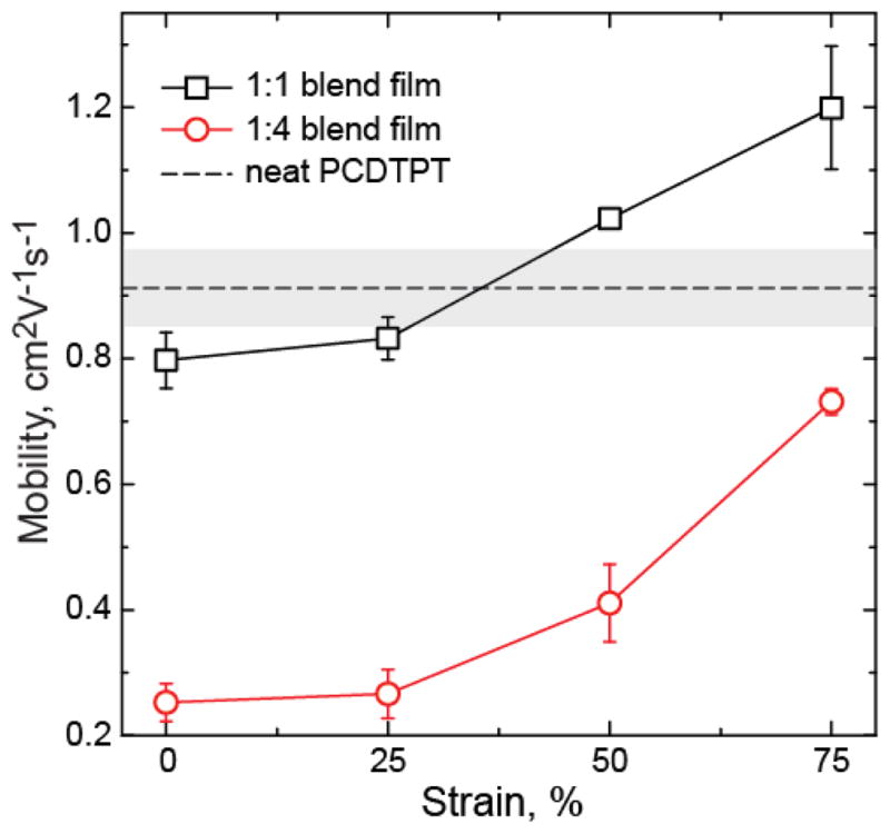
Saturated field effect mobility in the blend films with applied strained for charge transport parallel to the strain direction. The unstrained neat PCDTPT mobility is shown as a dotted line with uncertainty in gray, and is shown to compare to the strained films. The channel length of the devices was 5 μm.
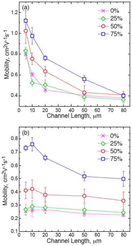
We see that the mobility increases with strain for both the 1:1 and 1:4 blend films with maximum achieved mobility values of 1.48 cm2V−1s−1 and 0.76 cm2V−1s−1, respectively. The strained 1:1 film achieves a mobility that surpasses the neat PCDTPT film. This increase in mobility with strain is commonly observed in strained polymer films, associated with alignment of the polymer backbone in the direction of strain.25,43 By increasing the ductility of the blend films, we are able to strain orient the polymer semiconductors and increase charge mobility. Here, we see that the relative increase in mobility of the 1:4 strained film is larger than the 1:1 film. The increase in mobility of the 1:1 film also appears to dampen at large strains. This is likely due to the nanoscale tearing that develops in the strained films. This is consistent with the channel length behavior in the strained films, shown in Figure 8. The relative mobility increase in the 1:4 strained films is similar for short and long channel lengths. In the 1:1 films, the long channel length mobility does not improve significantly with strain. This lack of improvement at large strains is likely associated with tearing in the primary transport material (PCDTPT). While charge transport is able to overcome small fracture features at short channel lengths and larger tearing features may be avoided, at long length scales the cumulative film discontinuity impedes improved carrier mobility. This channel length behavior is consistent with previous work on charge transport in the oriented pBTTT films, where film discontinuity limits long channel length mobility enhancement in oriented films.43 The larger increase in mobility with strain in the 1:4 films further supports that no significant fracture occurs in these film at large strains.
Figure 8.
Channel length dependence of the saturated mobility for various applied strains for transport parallel to the strain direction for (a) the 1:1 PCDTPT:P3HT blend films and (b) 1:4 blend film.
3. Conclusions
Methods to increase ductility of conjugated polymers have included the addition of small molecule additives,44 and to add disorder to the conjugated polymer backbone.45 Here, we have shown that the addition of a secondary polymer to the high mobility and stiff donor-acceptor polymer semiconductor PCDTPT can significantly increase the film ductility while maintaining charge transport characteristics. The ability to maintain charge transport behavior is attributed to vertical segregation of the high performance PCDTPT to the interface with the gate dielectric. The large increase in ductility is attributed to the fact that while vertical segregation is observed in the film, there is P3HT intermixed throughout the film thickness and the PCDTPT rich phase at the bottom of the film is not pure. Due to the increased ductility of the film, large strains were shown to orient both polymers in the direction of strain. The strain-oriented films were then shown to increase charge mobility in the direction of applied strain. The strain process enables the 1:1 blend film to achieve mobility values of 1.2 cm2V−1s−1 (with highest value obtained of 1.48 cm2V−1s−1) which is greater than the spun cast neat PCDTPT counterpart. The large increase in ductility observed in the polymer blend approach is a possible method to achieve stretchable polymer semiconductor films employing donor-acceptor polymers.
These results show that polymer blend films can be designed to retain the charge transport characteristics of the primary high mobility polymer semiconductor while also improving ductility associated with the secondary polymer. Thus, this work highlights the material opportunities for high performance polymer blend film transistors that are suitable for highly flexible and stretchable device applications. The improved mechanical behavior may also work in combination with other blend film advantages including optimized ink viscosity, reduced semiconductor consumption, improved lifetime, and self-patterning. Beyond polymer semiconductors, these results have significant implications on mechanical behavior of multi-component polymer thin films with vertically segregated character.
4. Experimental Methods
Film Preparation
The P3HT was obtained from Sigma Aldrich, Inc. with a number average molecular mass Mn = 54 kg/mol, polydispersity of 2.4 and a regioregularity of 0.99.46 The PCDTPT was synthesized using a previously described method, Mn = 103 kg/mol and polydispersity of 3.5.22 The neat P3HT and PCDTPT solutions and the blend solutions were dissolved in a solvent mixture of chloroform and dichlorobenzene at a 1:1 volume ratio at approximately 7 mg mL−1. Two PCDTPT:P3HT solutions were made with weight ratios of 1:1 and 1:4. All solutions were placed on a hot plate at 70°C for at least 24 h prior to processing. The solutions were spun cast at room temperature with a spinning rate of 1500(2π/60) rad s−1 (i.e. 1500 rpm) for 30 s onto OTS-modified silicon substrates with a native oxide layer (OTS-Si). This resulted in blend films of approximately 35 nm to 45 nm thick. The OTS treatment followed a previously described method.41 Large plastic strains were applied to the films by picking up from the donor OTS-Si substrate on PDMS and then applying the strain. Once the desired strain is reached, the films are then printed onto the secondary receiving substrate for further characterization, which included an OTS treated glass or Silicon substrate. The change in film thickness with applied strain can be estimated as t2 = t1/(1+ε)1−ν, where t2 is the final film thickness, t1 is the initial film thickness, ε is the applied strain, and ν is the Poisson’s ratio of the PDMS substrate, taken as 0.5.47
OTFT Fabrication and Electrical Characterization
The transistors had a bottom-gate bottom-contact configuration with Au source drain electrodes and a 200 nm SiO2 gate dielectric that was OTS treated. The neat PCDTPT films were directly cast on an OTFT test bed. The blend films were transfer printed from the initial casted substrate to the OTFT test bed using polydimethylsiloxane (PDMS) as the stamp. The transfer printing process follows a process previously described.35 All devices are thermally annealed at 200 °C for 5 min followed by slow cooling prior to device testing. The electrical properties were probed in a Nitrogen environment with a HP 4156B semiconductor parameter analyzer. For transfer characteristic, the gate voltage was swept from 20 V to −60 V for a drain source voltage of −60 V (saturation regime). Output characteristics were measured with gate voltages from 20 V to −60 V in steps of −20 V while sweeping the drain source voltage from 20 V to −60 V. The saturated field-effect mobility was calculated from a linear fit of ID1/2 versus VG, fitting a slope over a minimum 5 V range. The error bars are given as a standard deviation of a minimum of five measured devices.
Morphology Characterization
Contact angle measurements were performed with a Rame-Hart Inc. NRL C.A. Goniometer 100–00. AFM measurements were performed on a Bruker Dimension 3000 in tapping mode. The UV-Vis absorbance measurements were performed with an Ocean Optics Jazz spectrometer. X-ray diffraction measurements were performed at the Stanford Synchrotron Radiation Lightsource (SSRL) on beam line 11–3 with an area detector (MAR345 image plate), an energy of 12.735 keV, and an incidence angle of ≈0.12°. Samples were enclosed in a helium chamber to reduce air scattering and beam damage. The data was processed using previously published methods to convert detector images into intensity versus scattering angle, q.36,38,39 The XPS measurements were performed with a SPECS XPS with a 6 channel PHOIBIS 150 analyzer with pressure less than 3x10⁻¹⁰ Torr. Films were spun cast onto OTS Si then removed with carbon tape so that the bottom of the film was exposed for XPS measurements. The TOF-SIMS measurements were performed with ION TOF SIMS V instrument. The depth profiles were acquired with Cs ion beam sputtering and Bi ion beam analyzing.
Supplementary Material
Acknowledgments
This research work was supported by the National Science Foundation awards CMMI-1200340 and ECCS-1407885. Research at UCSB for the synthesis of PCDTPT was supported through the Mitsubishi Chemical Center for Advanced Materials (MC-CAM). X-ray diffraction was carried out at the Stanford Synchrotron Radiation Lightsource, a national user facility operated by Stanford University on behalf of the U.S. Department of Energy, Office of Basic Energy Sciences. TOF-SIMS, XPS, and AFM were carried out at the Analytical Instrumentation Facility at North Carolina State University. We thank Prof. Jan Genzer’s group of NC State University for assistance with contact angle measurements.
Footnotes
The following data are available free of charge: OTFT output curves of the 1:1 and 1:4 blend film, optical microscope images of blend films, XPS data of 1:4 blend film, 2D GIXD images of neat films and 1:4 blend film, AFM of strained 1:1 films.
References
- 1.Stingelin-Stutzmann N, Smits E, Wondergem H, Tanase C, Blom P, Smith P, De Leeuw D. Organic Thin-film Electronics from Vitreous Solution-Processed Rubrene Hypereutectics. Nat Mater. 2005;4(8):601–606. doi: 10.1038/nmat1426. [DOI] [PubMed] [Google Scholar]
- 2.Goffri S, Muller C, Stingelin-Stutzmann N, Breiby DW, Radano CP, Andreasen JW, Thompson R, Janssen RAJ, Nielsen MM, Smith P, Sirringhaus H. Multicomponent Semiconducting Polymer Systems with Low Crystallization-Induced Percolation Threshold. Nat Mater. 2006;5(12):950–956. doi: 10.1038/nmat1779. [DOI] [PubMed] [Google Scholar]
- 3.Arias AC. Vertically Segregated Polymer Blends: Their Use in Organic Electronics. Polym Rev. 2006;46(1):103–125. [Google Scholar]
- 4.Arias AC, Endicott F, Street RA. Surface-Induced Self-Encapsulation of Polymer Thin-Film Transistors. Adv Mater. 2006;18(21):2900. [Google Scholar]
- 5.Salleo A, Arias AC. Solution Based Self-Assembly of an Array of Polymeric Thin-Film Transistors. Adv Mater. 2007;19(21):3540. [Google Scholar]
- 6.Hamilton R, Smith J, Ogier S, Heeney M, Anthony JE, McCulloch I, Veres J, Bradley DDC, Anthopoulos TD. High-Performance Polymer-Small Molecule Blend Organic Transistors. Adv Mater. 2009;21(10–11):1166–1171. [Google Scholar]
- 7.Qiu LZ, Lee WH, Wang XH, Kim JS, Lim JA, Kwak D, Lee S, Cho K. Organic Thin-film Transistors Based on Polythiophene Nanowires Embedded in Insulating Polymer. Adv Mater. 2009;21(13):1349–1353. [Google Scholar]
- 8.Ferenczi TAM, Muller C, Bradley DDC, Smith P, Nelson J, Stingelin N. Organic Semiconductor: Insulator Polymer Ternary Blends for Photovoltaics. Adv Mater. 2011;23(35):4093. doi: 10.1002/adma.201102100. [DOI] [PubMed] [Google Scholar]
- 9.Lu GH, Blakesley J, Himmelberger S, Pingel P, Frisch J, Lieberwirth I, Salzmann I, Oehzelt M, Di Pietro R, Salleo A, Koch N, Neher D. Moderate Doping Leads to High Performance of Semiconductor/Insulator Polymer Blend Transistors. Nat Commun. 2013:4. doi: 10.1038/ncomms2587. [DOI] [PubMed] [Google Scholar]
- 10.Scaccabarozzi AD, Stingelin N. Semiconducting:Insulating Polymer Blends for Optoelectronic Applications-A Review of Recent Advances. J Mater Chem A. 2014;2(28):10818–10824. [Google Scholar]
- 11.Huang Y, Wen W, Mukherjee S, Ade H, Kramer EJ, Bazan GC. High-Molecular-Weight Insulating Polymers Can Improve the Performance of Molecular Solar Cells. Adv Mater. 2014;26(24):4168–4172. doi: 10.1002/adma.201400497. [DOI] [PubMed] [Google Scholar]
- 12.Smith J, Hamilton R, McCulloch I, Stingelin-Stutzmann N, Heeney M, Bradley DDC, Anthopolous TD. Solution-Processed Organic Transistor Based on Semiconductor Blends. J Mater Chem. 2010;20:2562–2574. [Google Scholar]
- 13.Moulton J, Smith P. Gel Processing of Electrically Conductive Blends of Poly(3-Octylthiophene) and Ultrahigh Molecular-Weight Polyethylene. J Polym Sci Pol Phys. 1992;30(8):871–878. [Google Scholar]
- 14.Muller C, Goffri S, Breiby DW, Andreasen JW, Chanzy HD, Janssen RAJ, Nielsen MM, Radano CP, Sirringhaus H, Smith P, Stingelin-Stutzmann N. Tough, Semiconducting Polyethylene-Poly(3-hexylthiophene) Diblock Copolymers. Adv Funct Mater. 2007;17(15):2674–2679. [Google Scholar]
- 15.Song E, Kang B, Choi HH, Sin DH, Lee H, Lee WH, Cho K. Stretchable and Transparent Organic Semiconducting Thin Film with Conjugated Polymer Nanowires Embedded in an Elastomeric Matrix. Adv Electron Mater. 2016;2 doi: 10.1002/aelm.201500250. [DOI] [Google Scholar]
- 16.Babel A, Jenekhe SA. Morphology and Field-Effect Mobility of Charge Carriers in Binary Blends of Poly(3-hexylthiophene) with Poly[2-methoxy-5-(2-ethylhexoxy)-1,4-phenylenevinylene] and Polystyrene. Macromolecules. 2004;37:9835–9840. [Google Scholar]
- 17.Biniek L, Schroeder BC, Nielsen CB, McCulloch I. Recent Advances in High Mobility Donor-Acceptor Semiconducting Polymers. J Mater Chem. 2012;22(30):14803–14813. [Google Scholar]
- 18.Sirringhaus H. 25th Anniversary Article: Organic Field-Effect Transistors: The Path Beyond Amorphous Silicon. Adv Mater. 2014;26(9):1319–1335. doi: 10.1002/adma.201304346. [DOI] [PMC free article] [PubMed] [Google Scholar]
- 19.Chortos A, Lim J, To JWF, Vosgueritchian M, Dusseault TJ, Kim TH, Hwang S, Bao ZA. Highly Stretchable Transistors Using a Microcracked Organic Semiconductor. Adv Mater. 2014;26(25):4253–4259. doi: 10.1002/adma.201305462. [DOI] [PubMed] [Google Scholar]
- 20.Savagatrup S, Printz AD, O’Connor TF, Zaretski AV, Lipomi DJ. Molecularly Stretchable Electronics. Chem Mater. 2014;26(10):3028–3041. [Google Scholar]
- 21.Wu HC, Benight SJ, Chortos A, Lee WY, Mei JG, To JWF, Lu CE, He MQ, Tok JBH, Chen WC, Bao Z. A Rapid and Facile Soft Contact Lamination Method: Evaluation of Polymer Semiconductors for Stretchable Transistors. Chem Mater. 2014;26(15):4544–4551. [Google Scholar]
- 22.Ying L, Hsu BBY, Zhan HM, Welch GC, Zalar P, Perez LA, Kramer EJ, Nguyen TQ, Heeger AJ, Wong WY, Bazan GC. Regioregular Pyridal[2,1,3]thiadiazole pi-Conjugated Copolymers. J Am Chem Soc. 2011;133(46):18538–18541. doi: 10.1021/ja207543g. [DOI] [PubMed] [Google Scholar]
- 23.Tseng HR, Ying L, Hsu BBY, Perez LA, Takacs CJ, Bazan GC, Heeger AJ. High Mobility Field Effect Transistors Based on Macroscopically Oriented Regioregular Copolymers. Nano Lett. 2012;12(12):6353–6357. doi: 10.1021/nl303612z. [DOI] [PubMed] [Google Scholar]
- 24.Virkar AA, Mannsfeld S, Bao ZA, Stingelin N. Organic Semiconductor Growth and Morphology Considerations for Organic Thin-Film Transistors. Adv Mater. 2010;22(34):3857–3875. doi: 10.1002/adma.200903193. [DOI] [PubMed] [Google Scholar]
- 25.O’Connor B, Kline RJ, Conrad BR, Richter LJ, Gundlach D, Toney MF, DeLongchamp DM. Anisotropic Structure and Charge Transport in Highly Strain-Aligned Regioregular Poly(3-hexylthiophene) Adv Funct Mater. 2011;21(19):3697–3705. [Google Scholar]
- 26.Gurau MC, Delongchamp DM, Vogel BM, Lin EK, Fischer DA, Sambasivan S, Richter LJ. Measuring Molecular Order in Poly(3-alkylthiophene) Thin Films with Polarizing Spectroscopies. Langmuir. 2007;23(2):834–842. doi: 10.1021/la0618972. [DOI] [PubMed] [Google Scholar]
- 27.Spano FC. Modeling Disorder in Polymer Aggregates: The Optical Spectroscopy of Regioregular Poly(3-hexylthiophene) Thin Films. J Chem Phys. 2005;122:23. doi: 10.1063/1.1914768. [DOI] [PubMed] [Google Scholar]
- 28.Klauk H, Schmid G, Radik W, Weber W, Zhou L, Sheraw CD, Nichols JA, Jackson TN. Contact Resistance in Organic Thin Film Transistors. Solid-State Electron. 2003;47:297–301. [Google Scholar]
- 29.Hamadani BH, Gundlach DJ, McCulloch I, Heeney M. Undoped Polythiophene Field-Effect Transistors with Mobility of 1 cm(2) V(−1) s(−1) Appl Phys Lett. 2007;91:24. [Google Scholar]
- 30.Bao Z, Dodabalapur A, Lovinger AJ. Soluble and Processable Regioregular Poly(3-hexylthiophene) for Thin Film Field-Effect Transistor Applications with High Mobility. Appl Phys Lett. 1996;69(26):4108–4110. [Google Scholar]
- 31.Heriot SY, Jones RAL. An Interfacial Instability in a Transient Wetting Layer Leads to Lateral Phase Separation in Thin Spin-Cast Polymer-Blend Films. Nat Mater. 2005;4(10):782–786. doi: 10.1038/nmat1476. [DOI] [PubMed] [Google Scholar]
- 32.Germack DS, Chan CK, Kline RJ, Fischer DA, Gundlach DJ, Toney MF, Richter LJ, DeLongchamp DM. Interfacial Segregation in Polymer/Fullerene Blend Films for Photovoltaic Devices. Macromolecules. 2010;43(8):3828–3836. [Google Scholar]
- 33.Campoy-Quiles M, Ferenczi T, Agostinelli T, Etchegoin PG, Kim Y, Anthopoulos TD, Stavrinou PN, Bradley DDC, Nelson J. Morphology Evolution via Self-Organization and Lateral and Vertical Diffusion in Polymer:Fullerene Solar Cell Blends. Nat Mater. 2008;7(2):158–164. doi: 10.1038/nmat2102. [DOI] [PubMed] [Google Scholar]
- 34.Sparrowe D, Baklar M, Stingelin N. Low-Temperature Printing of Crystalline:Crystalline Polymer Blend Transistors. Org Electron. 2010;11(7):1296–1300. [Google Scholar]
- 35.Boltau M, Walheim S, Mlynek J, Krausch G, Steiner U. Surface-Induced Structure Formation of Polymer Blends on Patterned Substrates. Nature. 1998;391(6670):877–879. [Google Scholar]
- 36.Baker JL, Jimison LH, Mannsfeld S, Volkman S, Yin S, Subramanian V, Salleo A, Alivisatos AP, Toney MF. Quantification of Thin Film Crystallographic Orientation Using X-ray Diffraction with an Area Detector. Langmuir. 2010;26(11):9146–9151. doi: 10.1021/la904840q. [DOI] [PubMed] [Google Scholar]
- 37.Muller-Buschbaum P. The Active Layer Morphology of Organic Solar Cells Probed with Grazing Incidence Scattering Techniques. Adv Mater. 2014;26:7692–7709. doi: 10.1002/adma.201304187. [DOI] [PubMed] [Google Scholar]
- 38.DeLongchamp DM, Kline RJ, Herzing A. Nanoscale Structure Measurements for Polymer-Fullerene Photovoltaics. Energy Environ Sci. 2012;5:5980–5993. [Google Scholar]
- 39.Kline RJ, Toney MF, McGehee MD. Highly Oriented Crystals at the Buried Interface in Polythiophene Thin-Film Transistors. Nature Mater. 2006;5:222–228. [Google Scholar]
- 40.O’Connor B, Chan EP, Chan C, Conrad BR, Richter LJ, Kline RJ, Heeney M, McCulloch I, Soles CL, DeLongchamp DM. Correlations Between Mechanical and Electrical Properties of Polythiophenes. ACS Nano. 2010;4(12):7538–7544. doi: 10.1021/nn1018768. [DOI] [PubMed] [Google Scholar]
- 41.Gargi D, Kline RJ, DeLongchamp DM, Fischer DA, Toney MF, O’Connor BT. Charge Transport in Highly Face-On Poly(3-hexylthiophene) Films. J Phys Chem C. 2013;117(34):17421–17428. [Google Scholar]
- 42.O’Connor BT, Reid OG, Zhang XR, Kline RJ, Richter LJ, Gundlach DJ, DeLongchamp DM, Toney MF, Kopidakis N, Rumbles G. Morphological Origin of Charge Transport Anisotropy in Aligned Polythiophene Thin Films. Adv Funct Mater. 2014;24(22):3422–3431. [Google Scholar]
- 43.Xue X, Chandler G, Zhang X, Kline RJ, Fei Z, Heeney M, Diemer PJ, Jurchescu OD, O’Connor BT. Oriented Liquid Crystalline Polymer Semiconductor Films with Large Ordered Domains. ACS Appl Mater Interfaces. 2015;7(48):26726–26734. doi: 10.1021/acsami.5b08710. [DOI] [PMC free article] [PubMed] [Google Scholar]
- 44.Savagatrup S, Chan E, Renteria-Garcia SM, Printz AD, Zaretski AV, O’Connor TF, Rodriquez D, Valle E, Lipomi DJ. Plasticization of PEDOT:PSS by Common Additives for Mechanically Robust Organic Solar Cells and Wearable Sensors. Adv Funct Mater. 2015;25(3):427–436. [Google Scholar]
- 45.Printz AD, Savagatrup S, Burke DJ, Purdy TN, Lipomi DJ. Increased Elasticity of a Low-Bandgap Conjugated Copolymer by Random Segmentation for Mechanically Robust Solar Cells. RSC Adv. 2014;4(26):13635–13643. [Google Scholar]
- 46.Certain commercial equipment, or materials are identified in this paper in order to specify the experimental procedure adequately. Such identification is not intended to imply recommendation or endorsement by the National Institute of Standards and Technology, nor is it intended to imply that the materials or equipment identified are necessarily the best available for the purpose.
- 47.Awartani OM, Zhao B, Curie T, Kline RJ, Zikry MA, O’Connor BT. Anisotropic Elastic Modulus of Oriented Regioregular Poly(3-hexylthiophene) Films. Macromolecules. 2016;49(327):327–333. [Google Scholar]
Associated Data
This section collects any data citations, data availability statements, or supplementary materials included in this article.


