Abstract
An 8-channel current steerable, multi-phasic neural stimulator with on-chip current DAC calibration and residue nulling for precise charge balancing is presented. Each channel consists of two sub-binary radix DACs followed by wide-swing, high output impedance current buffers providing time-multiplexed source and sink outputs for anodic and cathodic stimulation. A single integrator is shared among channels and serves to calibrate DAC coefficients and to closely match the anodic and cathodic stimulation phases. Following calibration, the differential non-linearity is within ± 0.3 LSB at 8-bit resolution, and the two stimulation phases are matched within 0.3%. Individual control in digital programming of stimulation coefficients across the array allows altering the spatial profile of current stimulation for selection of stimulation targets by current steering. Combined with the self-calibration and current matching functions, the current steering capabilities integrated on-chip support use in fully implanted neural interfaces with autonomous operation for and adaptive stimulation under variations in electrode and tissue conditions. As a proof-of-concept we applied current steering stimulation through a multi-channel cuff electrode on the sciatic nerve of a rat.
Index Terms: neurostimulator, electrical stimulation, neuromodulation, charge balancing, field steering, current steering DAC calibration, sub-binary radix
I. Introduction
Electrical stimulation is a widely used tool in basic and clinical neuroscience and neuroengineering. Common stimulation targets lie within the central and peripheral nervous system. Stimulation of the central nervous system (CNS) has been used to probe the functional role of populations of neurons, and provide sensory feedback to users of a neuroprosthetic device. Clinically, CNS stimulation is used to ameliorate symptoms of Parkinson’s disease, and epilepsy. Stimulation of the peripheral nervous system (PNS) has also been used to provide sensory feedback to users of prosthetic devices [1]. Emerging applications of PNS stimulation include treatment of hypertension and inflammatory disorders [2].
Designing neurostimulator circuits with very-large-scale-integration (VLSI) technology allows for the development of miniaturized, fully implantable systems, while simultaneously permitting the integration of extremely large numbers of channels, and increased functionality. Increased functionality means gains can be made in domains such as stimulation efficacy without compromising device size. This can be used to overcome limitations of electrical stimulation such as non-specificity.
It is straightforward to deliver electrical stimulation to target organs or neurons by placing electrodes within the proximity of the target. However, cell-types or tissue components cannot be selectively stimulated with electrical methods, as robustly as they can be with optical methods, which poses a challenge for therapeutic stimulation systems. Modifying the stimulus pulse shape or duration is one method for achieving more selective stimulation [3], [4]. Another degree of selectivity comes from the limited spatial extent of the induced electric field within tissue. Spatial patterns of stimulation, such as bipolar and tripolar, can be used to shape the electric field in-vivo to target groups of cells that are topographically segregated [5]. This has been leveraged in many neuroprosthetic applications such as cochlear implants, vestibular prostheses, visual prostheses, spinal stimulators, deep-brain stimulators, and peripheral nerve prosthetics [6], [7]. Due to its widespread use, VLSI neurostimulator systems should be designed to accurately stimulate in modes other than the standard monopolar and bipolar [8]–[10].
Additionally, circuits can be integrated with stimulator systems to ensure safety at the electrode-electrolyte interface. Chronic electrical stimulation can be damaging to both the electrode and tissue either through excitotoxic or electrochemical means [11]. Existing neural stimulators have addressed minimization of harmful electrochemical effects in several ways. Precise discrete components, or a capacitor in series with the output stage is one way to ensure no DC current flows through the electrode. A variety of ways amenable to VLSI implementation have also been proposed. Passive discharge is achieved by shorting the electrode to a reference voltage through a MOS switch, but due to the large RC time-constant associated with the electrode this can be a very slow process. An active discharge approach, i.e. driving the electrode to a reference voltage through a buffer, has similar effects as passive discharge, but limits the current that flows during the discharge phase [12]. Very precise charge balancing can be obtained using feedback that measures and dynamically matches the anodic current [13]. This method requires auxiliary amplifiers for every channel. An alternative strategy is to monitor the electrode voltage after stimulation, and use a feedback controller to update stimulation parameters or apply compensatory pulses [14]–[16]. By ensuring the electrode potential stays within safe limits, this approach prevents harmful charge buildup. In addition to the overhead required to implement the feedback loop, controller parameters must be tuned to obtain an acceptable transient response.
We propose an architecture that includes a single calibration circuit that is shared across all channels in the array. This support-circuitry performs three functions. First, it accurately ratios the currents across channels. Second, within channels, it matches the anodic and cathodic phases for charge balancing. Finally, it allows for blind calibration of each channel’s digital-to-analog converter (DAC). We provide results from a circuit fabricated in a commercial 180 nm CMOS process. Additionally, we use the proposed circuits to stimulate the sciatic nerve of anesthetized rats. By measuring the induced electromyogram (EMG), we demonstrate in-vivo effects of spatially patterned nerve stimulation.
This architecture, which includes the use of a sub-binary radix DAC and least-squares based calibration algorithm, was first introduced in conference form [17], and here we expand on these results. We provide more comprehensive descriptions and characterizations of the circuits and extensive in-vivo testing, demonstrating current steering stimulation applied to the sciatic nerve of rat.
II. Circuit Design
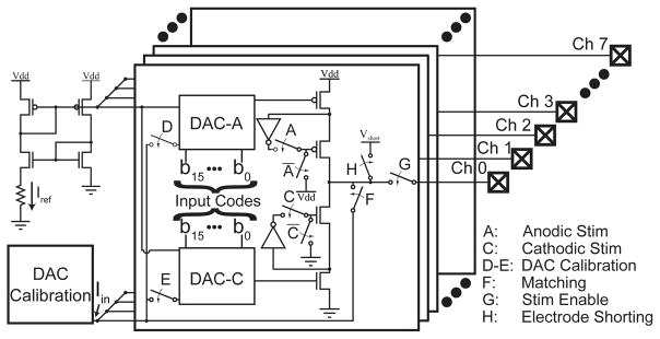
The block diagram of a single channel of our circuit is illustrated in Fig. 1. Two independent current-mode DACs supply biases to the current sources. The output of either DAC can be mirrored into the calibration circuit by closing switch D or E. Switches A and C activate anodic and cathodic stimulation respectively. Switch G disconnects current sources from electrodes. Closing switches A, C and F causes the difference in the anodic and cathodic currents to flow into the calibration circuit.
Fig. 1.
A block diagram for a single channel of the neural stimulator. Anodic and cathodic current sources have independent DACs which are routed to a calibration circuit for coarse calibration (switches D and E). When both current sources are simultaneously on, closing switch F allows the mismatch between the anodic and cathodic currents (the error current) to be measured by the calibration circuit. Switch H shorts the electrode to a reference voltage.
A. Digital-to-Analog Converter
DAC topologies used for neurostimulators include current steering DACs, implemented with binary [18] or unary [10] weighted current source arrays, and R-2R ladders [12]. An advantage of current steering DACs is that only the current sources needed for stimulation are switched on, whereas in a splitter the entire current is consumed regardless of the selected code. However, the area consumed by the weighted arrays increases exponentially with the number of bits, whereas the area of a splitter increases linearly. So for large number of bits, the weighted arrays occupy prohibitive amount of area.
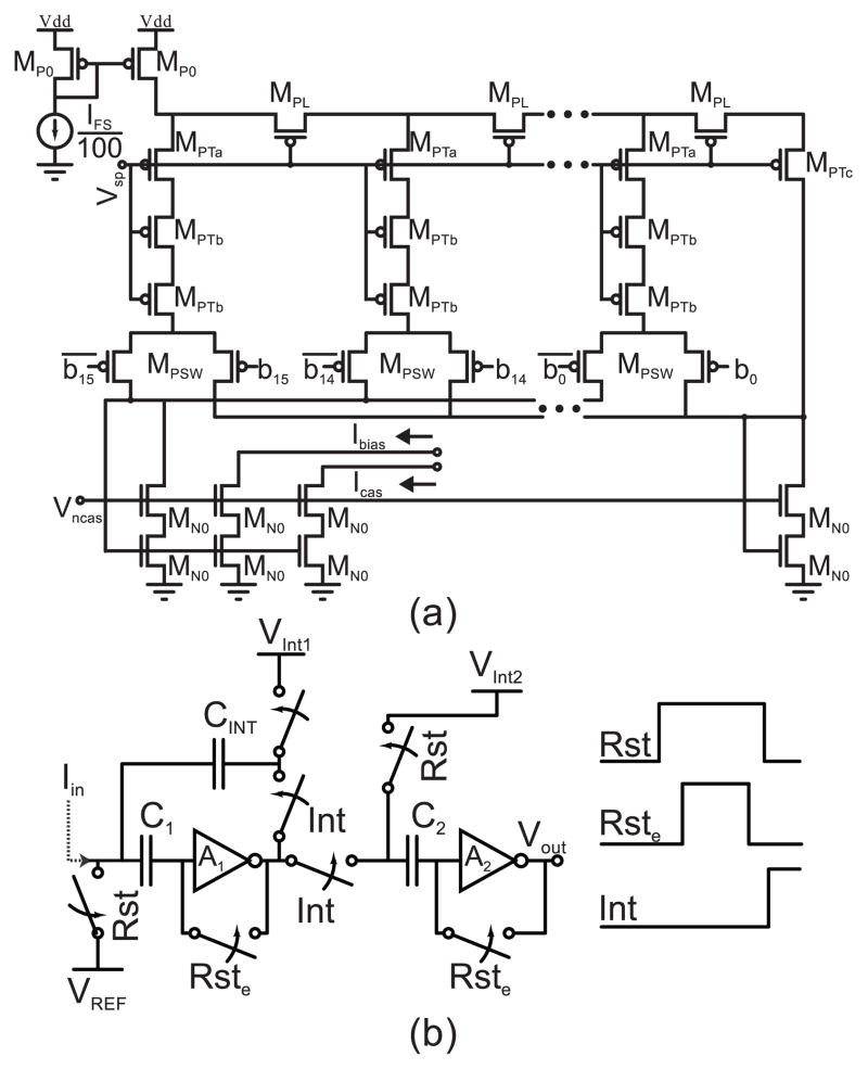
Both DACs (Fig. 2(a)) are 16-bit variations of the MOST R-2R structure [19]. The PMOS switches in Fig. 2(a) operate as switched cascodes. This helps reduce the sensitivity of the tap currents to the digital input code, which is important for the calibration procedure described later. Further, the increased lengths of the transistors in the vertical branches yield an R-βR structure, with β=2.5. At each node of an infinitely long R-βR ladder, if β >2, more current flows laterally than vertically through the respective tap. This introduces redundancies into the input-output relationship [20]. These redundancies can be removed via digital calibration [21].
Fig. 2.
(a) Circuit diagram for the R-βR splitter. (b) The calibration circuit consists of an integrator and comparator for an analog-to-time-to-digital conversion.
An external resistor sets the current reference to 1/100th of the fullscale stimulation level (IFS). This current is mirrored with unity-gain into each DAC. Two copies of the programmed current are mirrored out (Ibias and Icas in Fig. 2) to generate the voltage biases used in the output current buffer in Fig. 3. The total current consumed by the DAC and biasing network is 2 × IFS/100 + 8 × Istim/100
Fig. 3.
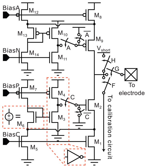
A modified regulated cascode, described in [22], serves as the output current source.
B. Calibration Circuit
The calibration circuit, shown in Fig. 2(b), consists of an integrator and a comparator described previously [23], [24]. Briefly, when Rst and Rste are high, the offsets of the inverters (common-source amplifiers, A1, A2) are stored on the capacitors in series with their inputs, the inverters are reset to their tripping point, and the integration capacitor is precharged. The offsets between Rst and Rste are to mitigate errors due to charge injection [22]. When Int goes high, CINT appears in parallel with A1, and the input current is integrated. When the output of A1 passes through VInt2, A2 trips. The time it takes for A2 to trip is quantified with a counter, digitizing the input current.
VInt1,2 are generated off-chip and set to 800 mV and 2.5 V to keep all devices in saturation during the integration. Their precise values do not matter, so they could be generated on-chip using a resistor string and a pair of buffers to drive the offset-storage capacitor and integration capacitor. The integration capacitor is 4.5 pF, providing an integration times greater than 3 μs. This analog-to-time-to-digital conversion is used in a calibration procedure described in Section III, and allows for the removal of the redundancies of the R-βR ladder. Additionally, Section IV describes how the measurement can be used to match the anodic and cathodic stimulation phases.
C. Biphasic Current Source
The output current sources are regulated cascodes; an additional branch (M5–M7 in Fig. 3) increases the output swing [22]. The gate of M3 is the input to a common source amplifier that provides output impedance boosting. Typically, this is connected to the drain of M1, which must stay in the vicinity of Vth, so that M3 is at least weakly inverted.
M7 and M4 are biased to source Istim/100 and Istim/50 respectively, and M5 is an additional finger of M1. M6 acts as a level-shifter, which allows the drain of M1 to drop to Vds,sat. Since Vds,1 is set to a value equal to the difference in Vgs between M3 and M6, the aspect ratios of M3,6 are set to provide sufficient Vds,1 for all output currents. The output swing of the current source is 2Vds,sat from each supply rail, and the devices were sized to give a Vds,sat of 120 mV and 150 mV for the NMOS and PMOS devices respectively. Maximizing output swing was a major concern, as large voltages can be developed across the electrode-electrolyte interface.
The feedback in regulated cascode circuits can lead to instability. M2 and M9 in Fig. 3 are driven by the feedback amplifiers, and are sized with a very large W/L (Table II) to minimize their Vds,sat. The large gate area provides a large load capacitance (400fF - 1pF depending on bias condition) to the feedback common-source amplifier which stabilizes the circuit [25].
TABLE II.
Transistor Sizing in the Current Buffer
| Transistor | W/L (μm) | Transistor | W/L (μm) |
|---|---|---|---|
| M1,2 | 200 × 1.5/1.4 | M8,9 | 300 × 0.95/0.71 |
| M5 | 2 × 1.5/1.4 | M12 | 3 × 0.95/0.71 |
| M3 | 4 × 2/2 | M10 | 16 × 1/1 |
| M6 | 12 × 2/2 | M13 | 48 × 1/1 |
| M4 | 2 × 1/2.5 | M11 | 15 × 1/5 |
| M7 | 1/2.5 | M14 | 5 × 1/5 |
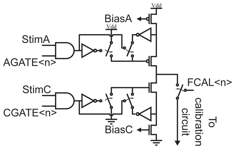
In practice, the signals that turn on the current sources (A and C in Fig. 3) are gated by the bits within two serially loaded registers, AGATE<0:7> and CGATE<0:7>. This configuration, shown in Fig. 4, permits the generation of arbitrary stimulation patterns.
Fig. 4.
The signals that activate the current sources, and connect the current sources to the calibration circuit are gated by a set of registers that are programmed serially.
III. Calibration Procedure
A sub-binary radix DAC can produce an analog output x, scaled from −1 to 1, from an n-bit binary code (here, n = 16) found through n iterations of the algorithm of Eqn. 1 [26]. In Eqn. 1, rk represents the residue at the kth step, and initialized to be x, bk is the kth bit in the binary code, and γk is the radix at the kth step.
| (1) |
For Fig. 2(a), γk is the ratio of currents flowing in adjacent vertical branches (tap currents). Therefore, to calibrate the DAC, we first obtain estimates of the tap currents.
The time Δt for a DC current source Iin to charge a capacitor CI from VInt1 to VInt2 is:
| (2) |
| (3) |
Here, b is a column vector of zeros and ones corresponding to the input binary code, and i is the column vector of tap currents. Combining Eqns. 2 and 3 gives Eqn. 4, where CI(VInt1 − VInt2) can be replaced by a single constant c1.
| (4) |
Eqn. 4 contains 16 unknowns (the 16 elements in i). For M DAC currents, the inverse of the integration times (Δt), obtained using the calibration circuit described in Section II-B, are stored in a vector f and the corresponding M input codes are stored in an M×16 matrix B. With M > 16, the system can be solved in the least squares sense. In practice, we make use of all 216 measurements for each DAC.
We chose to fit our solution to the differential linearity since it is much less affected by global nonlinearities which are approximately linear at small scales. Therefore, the inverse times in f and the rows of B are sorted in ascending order and adjacent values differenced yielding fΔ and BΔ respectively.
Then, the least squares estimate of the tap current coefficients, î is found by solving BΔi = c1fΔ
| (5) |
Since each γi is a ratio of the elements of î, the constant c1 cancels, except in the case of the MSB. For that case, γ15 is obtained by taking the ratio of i15 to the sum of the other elements of î. The precise values of γi do not matter if they are <2, providing a degree of insensitivity to the mismatch in the R-β R ladder of Fig. 2.
Here, the calibration procedure is initiated by an external FPGA which monitors and times the output of the comparator (Vout Fig. 2(b)). Integration times are uploaded to a PC which obtains the least-squares solution. In practice, the system need not be connected to a PC. Calculation of the DAC coefficients (γ0 - γ15) could be performed once by a low power FPGA or microcontroller using the recursive least-squares algorithm (RLS). With the calculated γ’s, the proper input code for a given output is obtained from 16 iterations of Eqn 1.
IV. Matching
A. Charge Balancing
Matching the two stimulation phases is performed by activating both current sources and closing switch F in Fig. 1. The difference between the two currents, the error current, will flow into the integrator in Fig. 2(b). The matching procedure consists of two steps.
First, VInt1andVInt2 are set equal, and an integration is triggered. The state of Vout reflects the polarity of the error current. For example, if the anodic current is larger than the cathodic current, the output of the integrator will fall, and Vout will hit the positive rail (Vout = 1). Likewise, if the cathodic current is larger, the output of the integrator will rise and Vout will hit the negative rail (Vout = 0).
Next, VInt1 ≠ VInt2; if at the end of step 1, Vout = 1, then VInt1 > VInt2, and vice versa. When an integration is triggered, the time it takes for the comparator to trip is inversely proportional to the error current. Therefore, the error current integration is timed and the input code to one of the DACs is adjusted until the error current is minimized.
The integration time for matching is bounded only by leakage currents, which should cause the comparator to trip over time scales of seconds. Therefore, in software a timeout of 150 ms is enforced. Furthermore, to facilitate a quick matching procedure, a successive approximation strategy is used, where the outcome of step 1 is used to determine the state of a given bit in the binary code, and at the end, the code with the maximum integration time is selected.
B. Current Steering
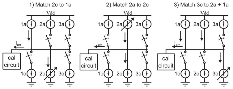
The above procedure can be generalized to match stimulation across channels, allowing the circuit to operate in bipolar stimulation mode, or to create complex current-steering stimulation patterns. Fig. 4, illustrates a single stimulator channel with the control signals that are arrayed across all channels. An 8-bit serially loaded register FCAL controls the switches (switch F in Fig 1) that route currents to the calibration circuit. Along with the gating discussed in Section II-C, arbitrary combinations of channels can be matched by connecting all active channels to the calibration circuit simultaneously, and asserting the required gating bits.
For example, a tripolar configuration consists of one cathodic channel sinking a current of Ic, counterbalanced by two anodic channels, each sourcing a current Ia = Ic/2. Fig. 5 depicts how a tripolar stimulation pattern can be generated in three steps. In steps 1 and 2, the anodic channels (1a and 2a) are indirectly matched to each other. In the third step, the cathodic channel (3c) is matched to their sum.
Fig. 5.
The calibration circuit can be used to generate spatial stimulation patterns. Here, a tripolar pattern can be generated by first matching the anodic phases of two channels, then matching the cathodic phase of a third channel to their sum.
This procedure fixes the digital codes for the anodic sources of channel 1 and 2, and the cathodic source of channel 3. The complementary DACs must then be tuned for in-channel charge balance.
V. Electrode Interface
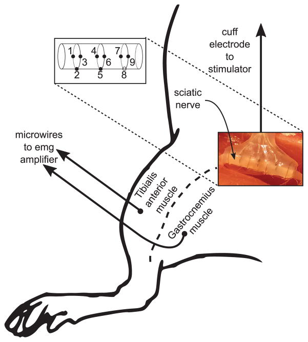
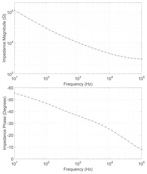
We interfaced our stimulator to concentric cuff electrodes (MicroProbes for Life Science, Gaithersburg, MD). Each cuff contained nine 125 μm diameter stainless steel contacts, with three groups of three electrodes arranged circumferentially, 90 degrees apart, and with each group spaced 2.5 mm apart (Fig. 13 (inset)). These electrodes, when used for acute, small-animal studies, and at low current levels (≤ 250 μA), do not require high voltage transistors or special circuit techniques to prevent oxide breakdown or hot-carrier effects. Figure 6 illustrates impedance magnitude and phase data for a single electrode from the cuff array.
Fig. 13.
Experimental setup for in-vivo testing. A multi-channel concentric cuff was interfaced to the sciatic nerve of a rat. The electrode consisted of three concentric triplets for a total of nine electrodes, and eight of the nine electrodes (solid circles in inset) were connected to the neurostimulator chip. Microwires were inserted into two muscle groups (tibialis anterior and gastrocnemius) to record intramuscular EMG in response to stimulation.
Fig. 6.
Impedance data for a single stainless-steel electrode from the cuff array used to interface the stimulator in-vivo
VI. Benchtop Characterization
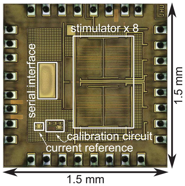
An eight channel version of the neural stimulator was fabricated in a 0.18 μm CMOS process. A micrograph of the 1.5 mm × 1.5 mm chip is illustrated in Fig 7. Each stimulator channel, including DACs, occupied an area of 290 μm × 220 μm, and the calibration circuit occupied 200 μm × 70 μm. Additionally, an SPI interface was synthesized from a standard cell library. The remaining area consists of metal fill.
Fig. 7.
Micrograph of an eight-channel stimulator, fabricated in a 0.18 μm CMOS process. The die size including pads measures 1.5 ×1.5 mm2
A. DAC Calibration
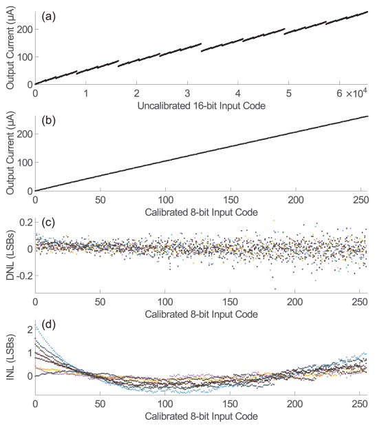
Fig. 8(a,b) shows the digital input - analog output relationship before and after calibration for a single channel. The pre-calibration non-monotonicity is by design and clearly evident, and the procedure described in Section III was used to remove the redundancies. The measured differential nonlinearity (DNL) and integral non-linearity (INL) for all channels are summarized in Fig. 8(c,d). The worst case DNL was 0.3 LSBs, and the mean absolute value was <0.04 LSBs. INL was defined as the difference between the actual output and the best-fit line. The worst case INL was measured to be 2.2 LSBs, and the mean absolute value was <0.3 LSBs. Currents were measured with a Keithley 6430 Source Measurement Unit.
Fig. 8.
Input output relationship of the DAC before (a) and after calibration (b). Linearity is quantified by the differential non-linearity (DNL)(c) ≤0.3 LSBs and the integral non-linearity (INL)(d) <3 LSBs. Points represent data across 8 channels.
Integration times ranged from 3 μs to 30 ms, and the calibration process for each DAC, took on average less than 9 seconds. Calibration of all 16 DACs took 140 seconds.
B. Matching
The matching error was determined by measuring the mean residual voltage left on a 100 nF capacitor following four biphasic 200 μs pulses, and normalizing that value to the peak capacitor voltage at full-scale. The capacitor voltage was buffered by an off-the-shelf CMOS op-amp (AD8608, Analog Devices, Norwood, MA), and digitized by a DAQ with a 16-bit A/D converter (NI USB 6251, National Instruments, Austin, TX). The capacitor voltage was sampled at 1 MHz for 150 us before and after each biphasic pulse. Each set of 150 samples were averaged, and the difference gave the voltage error, which was then referred back to an equivalent error current. For each measurement, the dynamic range of DAQ was set to the minimum necessary to accommodate the peak capacitor voltage on that trial to mitigate the effects of measurement noise. This ranged from ±0.1 V (the device minimum) to ±1 V.
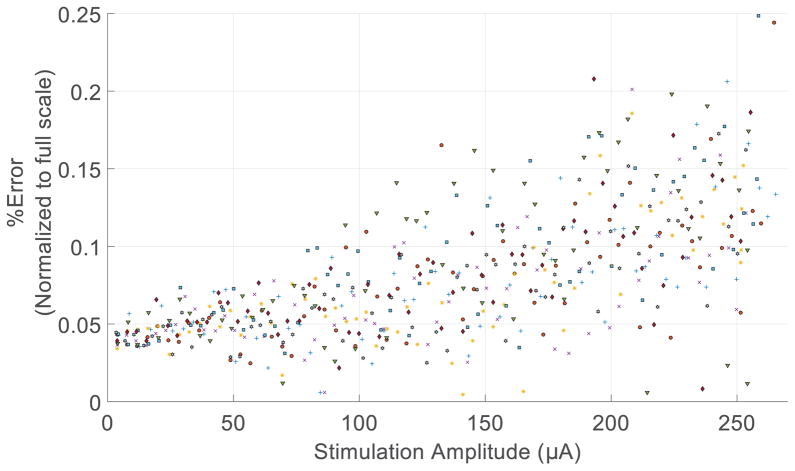
Fig. 9 illustrates the error currents after matching, normalized to the full-scale current output. We performed this measurement only on a subset of calibrated DAC values. For each channel 64 measurements were made instead of all 256. The worst-case error is less than 0.3% of the full-scale current, comparable with other state-of-the-art designs [27], [28].It typically takes less than 200 ms to find the closest match.
Fig. 9.
The difference between the anodic and cathodic currents normalized to the full scale current.
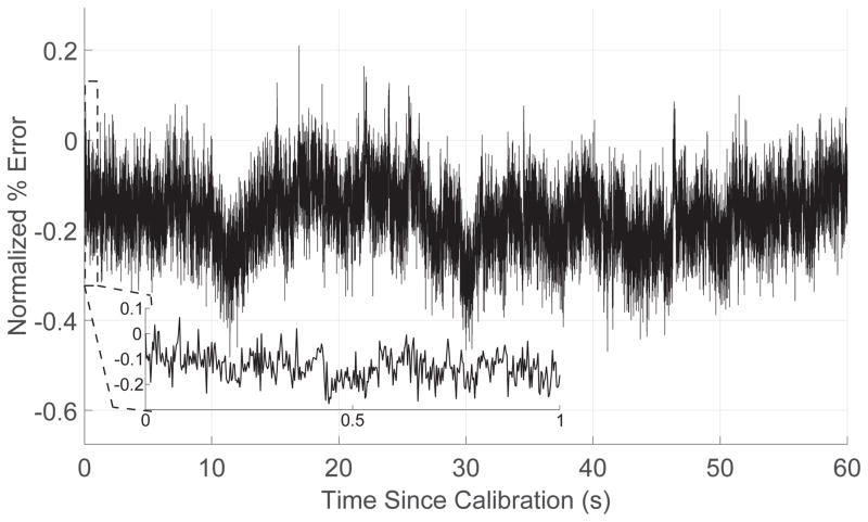
One advantage of this design is that once matching is performed, the parameters can be stored digitally. However, this also leads to a potential limitation in its sensitivity to 1/f noise. To evaluate this possibility, we continuously applied 250 μA pulses to a capacitor over the course of 60 seconds, measuring the residual voltage after each pulse. The pulse widths were 200 μs, and the pulse rate was 400 Hz, for a total of 24,000 pulses. After each pulse, a 200 μs delay was added to allow calculation of the residual voltage in post-processing, and then the shorting switch was closed to bring the capacitor voltage back to baseline before the next pulse.
Fig 10 shows the residual capacitor voltage, normalized to the peak voltage, over time. The error over all 24,000 pulses had a mean and standard deviation of 0.17% and 0.07%; over the first 400 pulses (Fig. 10 inset) the mean and standard deviation were 0.12% and 0.06%.
Fig. 10.
Variation in the matching between anodic and cathodic currents over time.
C. Current Steering
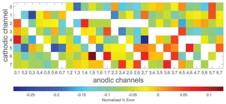
The accuracy of current steering was similarly also evaluated. Here, error was determined by shorting all channels to a single 10 nF capacitor and measuring the voltage on the capacitor during the inter-pulse interval. Fig. 11 shows the measured error from matching a tripolar configuration (Fig. 5). The rows of Fig. 11 correspond to the channel selected as the cathodic sink (Ic = 250 μA). The columns correspond to different channel pairs that complete the tripolar unit. There are 28 possible pairs of channels, 7 of which include the channel used as the cathodic sink (white entries). As with charge balancing, the errors were measured < 0.3%.
Fig. 11.
The percent difference between the stimulating cathodic current and a pair of anodic channels. The y-axis indicates the channel selected as the cathodic source, and the x-axis corresponds to the different pairs of channels that complete the tripolar unit. White entries correspond to combinations where the cathodic channel and anodic pair conflict.
VII. In-vitro Results
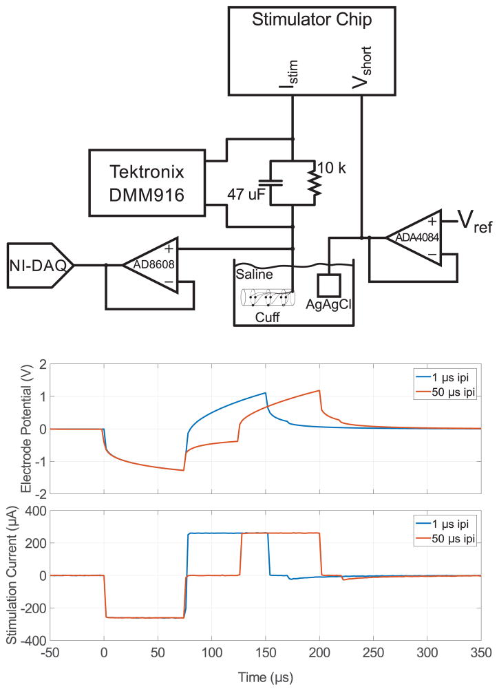
We used the setup depicted in Fig. 12(a) to evaluate the effective DC current when stimulating through electrodes. We measured the effective DC level for 250 μA, 75 μs stimulation at 500, and 1000 Hz, with two inter-pulse-intervals (1 μs and 50 μs). Matching was performed immediately before the pulse train started, and the shorting switch was activated in between biphasic pulses. No re-calibration was made during this interval. Fig. 12(b) shows the time-domain stimulation waveform recorded during this measurement. The DC measurement was given 1 minute to settle; the values listed in Table III lists the maximum DC measured by the DMM thereafter as well as the current density given the 0.0123 mm2 electrode surface area. To evaluate the effect of 1/f noise in-vitro, the 1000 Hz, 50 μs ipi measurement was taken out to 10 minutes. Throughout the test, the maximum and minimum measurement was 5 nA and 3 nA respectively, with the mean shifting slightly from 5 nA to 4 nA after 5 minutes.
Fig. 12.
Experimental setup for in-vitro testing. A parallel RC was placed in series with the stimulator and the cuff electrode array submerged in saline along with an AgAgCl return electrode. A Tektronix digital multi-meter (DMM) measured the average voltage across the RC to record the effective DC current. The electrode potential time-domain waveform and current profile are shown below. A CMOS input op-amp was used to buffer the electrode waveform and digitized with a 16-bit NI-DAQ. Two waveforms are shown, one with a 1 μs inter-pulse interval (ipi) and the other with a 50 μs ipi. The current profile was measured by replacing the parallel RC with a single 100 Ω resistor, adding a second buffer, and feeding the two buffered waveforms into the DAQ to be read differentially.
TABLE III.
Effective DC measured in-vitro
| Frequency (Hz) | Inter-pulse interval (μs) | DC (nA) | Current density (nA/mm2) |
|---|---|---|---|
| 500 | 1 | 2 | 163 |
| 500 | 50 | 3 | 244 |
| 1000 | 1 | 3 | 244 |
| 1000 | 50 | 5 | 407 |
VIII. In-vivo Results
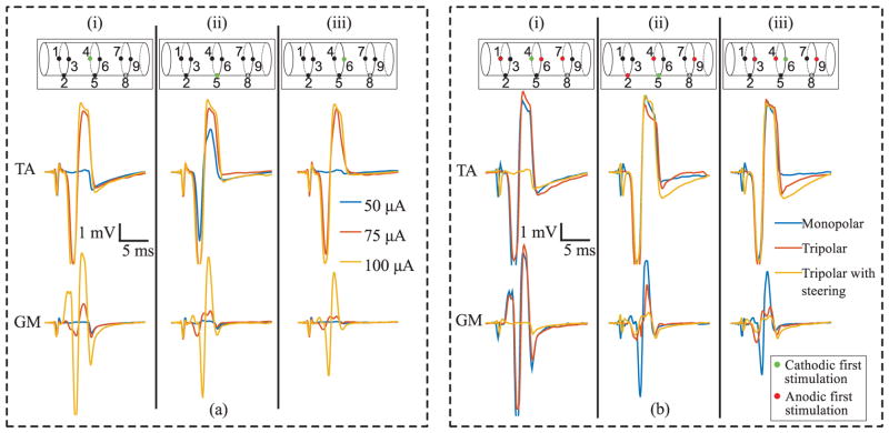
To test the stimulator in-vivo, we interfaced the cuff electrode described in Section V to the sciatic nerve in a rat, and recorded electromyogram (EMG) signals from the tibialis anterior (TA) and gastrocnemius (GM) muscles of the lower leg (Fig. 13). Male Wistar rats weighting 300–320 g were used in this experiment. All procedures were approved by Johns Hopkins Medical Institute Animal Care and Use Committee (ACUC). Each rat was implanted under 2% isoflurane anesthesia with a nose cone. After swabbing the dissection area with 70% ethanol, the skin was cut along the back of the thigh. The left sciatic nerve was dissected at the midthigh and carefully freed from surrounding tissues from the sciatic notch to the knee. The cuff electrode was opened and placed around the sciatic nerve avoiding compression and stretch. To record EMG activity, pairs of fine wire hook electrodes (two 40-gauge Teflon-coated steel wires in a 27-gauge 12.5 mm hypodermic needle) were implanted in the left gastrocnemius (GM) and tibialis anterior (TA) muscle; signals were amplified and digitized with an RA16PA preamplifier (Tucker-Davis Technologies, Alachua, FL). All EMG responses plotted in Figs. 14, 15 are averages of five responses.
Fig. 14.
In-vivo recorded physiological response to spatially patterned nerve stimulation in anesthetized rat. In all plots, insets indicate the electrodes used, and the polarity of stimulation at those sites. Green indicates cathodic first, and red indicates anodic first. (a) EMG response of the tibialis anterior (TA) muscle (top row) and the gastrocnemius (GM) muscle (bottom row) to monopolar stimulation of the three center-ring electrodes at three levels of stimulation. (b) EMG response of TA (top row) and GM (bottom row) to three patterns of stimulation at 100 μA.
Fig. 15.
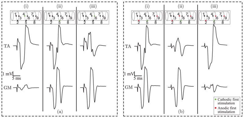
EMG response to stimulation of the sciatic nerve in the TA (top row) and GM muscles (bottom row). (a) Columns i–iii show responses due to monopolar stimulation at the three center contacts. (b) Column i shows the response to a tripolar stimulation pattern, with electrode 5 used as the cathodic contact, and columns ii–iii show the altered response when an anodic steering contact is added at electrodes 4 and 6 respectively. The anodic contact at electrode 4 attenuates the TA response while the anodic contact at electrode 6 attenuates the GM response.
The EMG response from monopolar stimulation of each of the center triplet’s contacts is depicted in Fig. 14(a). Stimulation consisted of single pulses with a 75 μs pulse width, and a 50 μs inter-pulse interval. The current’s return path was through a stainless steel needle electrode in the neck. Electrode 5 showed the highest sensitivity for TA; a 50 μA pulse was sufficient to evoke an EMG response, while no response was seen in GM. A 75 μA pulse was needed at electrodes 4 and 6 to evoke a response, but each site still appeared selective to TA. At each site, the non-specificity of stimulation prevented the stimulator from inducing the maximal response from TA without activation of GM.
Current steering stimulation patterns were applied to assess how EMG responses might be altered. Fig. 14(b) compares the EMG response to three stimulation patterns, monopolar, tripolar, and tripolar with an additional current steering contact. The tripolar pattern consisted of the middle contact activated cathodic first (primary electrode), and the two adjacent electrodes activated anodic first, calibrated with an amplitude of 1/2 as described in Section IV. The tripolar with current steering pattern was identical to the tripolar pattern, but with an additional second center contact activated anodic first with an amplitude matched to the primary electrode. Patterned stimulation at electrodes 5 and 6 had a clear effect on the evoked response. At electrode 4, the additional anodal contact suppressed an EMG response within both muscles; while not useful in practice, it is shown here for completeness.
Fig. 15 illustrates another example of the physiological effects of using the circuit for current steering stimulation. In this experiment, performed in a different rat, stimulation again consisted of single pulses. We used a 50 μs pulse width, and a 50 μs inter-pulse interval. Due to the decreased pulse width selected a slightly higher amplitude of 150 μA was required to evoke maximal EMG responses. Fig. 15(a) shows the effects of monopolar stimulation to the three center contacts. Contact 4 was preferential to the TA muscle, contact 6 was preferential to the GM muscle, and contact 5 exhibited no preference. Fig. 15(b) illustrates the effects of steering. Columns i–iii depict the EMG response to tripolar stimulation with (i) no steering contact, (ii) electrode 4 as an anodic steering contact, and (iii) electrode 6 as an anodic steering contact. Steering with electrode 4 suppressed the EMG response in the TA muscle, while steering with electrode 6 suppressed the EMG response in the GM muscle.
IX. Discussion
A. DAC Calibration
The post-calibration resolution of the DACs is limited to 8-bits. One likely cause is that the tap currents vary significantly with the input code. Interestingly, we have found the lower order bits seem to provide no additional benefit here. For example, running the algorithm on the upper 12 bits, leaving the lower 4 bits set to 0 provides the same level of accuracy and precision. However, presently, this is not much of a concern as most neurostimulator designs make use of only 5 to 6 bits (Table IV). Given that the precision of matching can exceed 0.3%, the lower bits do provide a benefit for charge balancing.
TABLE IV.
Comparison of this work with the state-of-the-art
| Parameter | This Work | [37] | [10] | [18] | [28] | [38] | [27] | [14] | [13] |
|---|---|---|---|---|---|---|---|---|---|
| Year | 2016 | 2015 | 2015 | 2014 | 2014 | 2013 | 2013 | 2012 | 2007 |
| Technology | 0.18 μm | 0.18 μm HV |
0.5 μm HV |
65 nm | 0.35 μm HV |
0.18 μm HV |
65 nm | 0.35 μm HV |
0.7 μm HV |
| Supply Voltage (V) | 3.3 | 18 | 12 | 3 | 15 | 12 | ±2.5 | 20 | +6/−9 |
| Number of Channels | 8 | 1 | 16 | 256 | 2 | 8 | 512 | 2 | 1 |
| Max Istim (mA) | 0.25 | 1.05 | 1.45 | 0.465 | 1 | 0.504 | 0.05 | 1 | 1 |
| Resolution (ENOB) | 8 (7.4) | 7 (-) | 9 (8) | 5 (4.3) | 5 (4.6) | 6 (-) | 5 (-) | 5 (-) | 7 (-) |
| Charge balance architecture | biphasic + calibration | H-bridge | current mirror | dynamic current mirror | dynamic current mirror | asymmetric H-bridge | biphasic + calibration | pulse insertion, offset regulation | dynamic current mirror |
| Matching (%) | 0.3 | <0.01 | 3.6 ±2.5 | 0.5 | 0.1 | 0.05 | 2.24 | N.A. | 0.4 |
| Stimulation Modes | multipolar | monopolar, bipolar | multipolar | multipolar | monopolar | bipolar | monopolar | monopolar | monopolar |
A limitation of the proposed calibration technique is that a linear regression is required to compute DAC coefficients. While an on-chip implementation of the recursive least squares algorithm is not prohibitive, it would be far more economical to have an FPGA or microcontroller compute the coefficients in the background and communicate them back to the stimulator chip.
B. Matching
The offline calibration strategy proposed here achieves a precision of 0.3% in matching of the anodic and cathodic phases. The use of an interpulse delay allows charge stored in the double-layer capacitance to be lost through faradaic reactions, but the inclusion of a passive discharge switch compensates.
The 1/f noise in the current sources and biasing network increases the variance of this measurement. To assess the long-term implications, we directly measured the DC current flowing through a cuff electrode in-vitro over ten minutes [29], [30], and found only a 1 nA shift in the baseline. With recalibration performed every 10 minutes and 200 ms required per channel, the calibration circuit would need to operate with a duty cycle of only 0.27%.
Reported safe current densities for effective DC in-vivo range from 230 nA/mm2 [31] to 750 nA/mm2 [32]. The maximum effective DC level measured here (407 nA/mm2) falls within this range. Note that this DC level was measured with 1000 Hz stimulation, a much higher frequency than would be used in virtually any stimulation application. However, our measurement setup had a minimum detectable level of 1 nA, so high stimulus rates were required to drive the measured DC well above 1 nA. For the low stimulus rates used here, passive discharge alone may have been sufficient to reduce net DC down to what are considered safe levels. Balanced biphasic stimulation confers an additional safety margin, and may be necessary in a chronically implanted system where electrode-tissue impedances can change over time.
C. In-vivo results
The results of Section VIII demonstrated altered physiological responses to current steering stimulation patterns. The parameter space for current steering stimulation is extensive, and we have not undertaken an exhaustive search for optimal patterns. The stimulation patterns tested here were based off of previous studies in similar animal models, and have rigorously demonstrated the enhanced selectivity obtained through current steering [5], [33]–[35]. This is an active and promising area of research, and progress will likely rely on both novel hardware as well as mathematical modeling of the electric field profile in tissue [36].
One limitation was large variability between the two animals tested. For the first rat, were unable to find any configurations (neither monopolar nor multipolar) that were selective for GM. The results from the second rat show that multi-electrode arrays themselves can offer some degree of selectivity. For the second rat both monopolar and multipolar configurations could be selective for GM and TA. Therefore, these results only serve to demonstrate feasibility.
Inter-animal variability was likely due to a combination of variations in nerve cuff electrode orientation and fine-wire electrode placement within the muscles of interest. In particular, fine-wire electrodes have a small conduction volume that can sensitively collect even individual motor unit action potentials. Therefore, despite consistent placement within a specific muscle of interest, variations in the composition of motor units, in terms of muscle type and patterns of activation, may influence the output recorded by a fine-wire electrode. Future experiments could mitigate this effect through the use of multiple fine-wire electrodes, and taking either averaged measurements across the electrodes or differences between electrodes to capture higher conduction volumes. Additionally, prior work in the field have used cuff electrodes with contacts spanning the entire circumference of the nerve [5], [33], [34], whereas here the arrays used covered 75% of the nerve circumference, in the future, histological examination of the stimulated tissue should be made to validate.
D. Comparison with the state-of-the-art
Table IV lists the specifications from this work along with six other published works. This work, as well as that of [10] and [18] demonstrate multipolar stimulation, but rely on inter-channel matching for the accuracy of such patterned stimulation, whereas here, a calibration method ensures such accuracy. Any neurostimulator system with multiple of independent current sources can be used as a current-steering stimulator. The methods proposed here offer a way to ensure the accuracy of such stimulation waveforms. Furthermore, the overhead to accomplish this is shared with a method to improve charge balance. However, the precision necessary to ensure the desired in-vivo effect (in this case the specificity of stimulation) remains to be demonstrated. The works that have leveraged multipolar stimulation tend to make use of a separate source and sink per channel. A VLSI systems based on the H-bridge architecture, designed for multipolar stimulation, was presented in [39]. This work used a switch network connecting a single current source to two blocks of 50 electrodes. Current could be passed from any single member of one block through any arbitrary combination of electrodes in the opposing block.
Charge balancing accuracy trends can also be gleaned from Table IV. As noted in [37], the H-bridge architecture is intrinsically charge balanced; the same current source is used for both phases of stimulation. As such, this architecture tends to achieve charge-balance accuracy an order of magnitude greater than other methods. The calibration method described here achieves similar accuracy to the dynamic current mirror method. Both methods null the error between anodic and cathodic phases; the dynamic current mirror does so using analog feedback and a storage capacitor, whereas we use a digital feedback loop, storing the result in a digital register. The use of an additional “shorting” switch in each channel allows for DC current levels to be brought well below safety-limits [13], [18], [28].
X. Conclusion
We have presented an architecture for a current steering neurostimulator array. An on-chip calibration circuit facilitates spatial patterning of the electric field in-vivo and additionally is used to calibrate an 8-bit current-mode DAC for each channel, as well as charge balance biphasic stimulation. The calibration circuitry is shared across channels, and therefore the architecture is particularly suited for high channel-count systems. Further, since charge balancing is achieved without off-chip components the system is amenable to implantable systems. Spatial patterning of electrical stimulation offers a method to activate specific targets in-vivo, a major obstacle in the development of low-side-effect neurotherapeutic stimulation systems
TABLE I.
Transistor Sizing in the R-βR Splitter
| Transistor | W/L (μm) |
|---|---|
| MP0 | 4 × 3.6/3.6 |
| MPL | 0.84/0.4 |
| MPTa | 0.84/0.4 |
| MPTb | 0.84/0.3 |
| MPTc | 0.84/0.52 |
| MPSW | 2 × 0.84/0.6 |
| MN0 | 2 × 2.36/2.36 |
Acknowledgments
This work was supported in part by the National Institutes of Health RO1HL071568 and T32EB005176, and in part by the National Science Foundation EFRI-M3C 1137279
Drs. Phillipe Pouliquen, Kartik Murari and Mohsen Mol-lazadeh provided valuable input on circuit design and characterization.
Contributor Information
Elliot Greenwald, Department of Biomedical Engineering, Johns Hopkins School of Medicine, Baltimore, MD, 21205 USA.
Christoph Maier, Department of Bioengineering, and Institute for Neural Computation, University of California San Diego, La Jolla, CA 92093 USA.
Qihong Wang, Department of Biomedical Engineering, Johns Hopkins School of Medicine, Baltimore, MD, 21205 USA.
Robert Beaulieu, Department of Biomedical Engineering, Johns Hopkins School of Medicine, Baltimore, MD, 21205 USA.
Ralph Etienne-Cummings, Department of Electrical and Computer Engineering, Johns Hopkins University, Baltimore, MD, 21218 USA.
Gert Cauwenberghs, Department of Bioengineering, and Institute for Neural Computation, University of California San Diego, La Jolla, CA 92093 USA.
Nitish Thakor, Department of Biomedical Engineering, Johns Hopkins School of Medicine, Baltimore, MD, 21205 USA. Singapore Institute for Neurotechnology, National University of Singapore, Singapore 119077.
References
- 1.Nag S, Thakor NV. Implantable neurotechnologies: electrical stimulation and applications. Medical & Biological Engineering & Computing. 2016;54(1):63–76. doi: 10.1007/s11517-015-1442-0. [DOI] [PubMed] [Google Scholar]
- 2.Famm K, Litt B, Tracey KJ, Boyden ES, Slaoui M. Drug discovery: a jump-start for electroceuticals. Nature. 2013;496(7444):159–161. doi: 10.1038/496159a. [DOI] [PMC free article] [PubMed] [Google Scholar]
- 3.Fang ZP, Mortimer JT. Selective activation of small motor axons by quasitrapezoidal current pulses. IEEE Transactions on Biomedical Engineering. 1991 Feb;38(2):168–174. doi: 10.1109/10.76383. [DOI] [PubMed] [Google Scholar]
- 4.Grill WM, Mortimer JT. The effect of stimulus pulse duration on selectivity of neural stimulation. IEEE Transactions on Biomedical Engineering. 1996 Feb;43(2):161–166. doi: 10.1109/10.481985. [DOI] [PubMed] [Google Scholar]
- 5.Sweeney J, Ksienski D, Mortimer J. A nerve cuff technique for selective excitation of peripheral nerve trunk regions. Biomedical Engineering, IEEE Transactions on. 1990 Jul;37(7):706–715. doi: 10.1109/10.55681. [DOI] [PubMed] [Google Scholar]
- 6.Eiber CD, Lovell NH, Suaning GJ. Attaining higher resolution visual prosthetics: a review of the factors and limitations. Journal of Neural Engineering. 2013;10(1):011002. doi: 10.1088/1741-2560/10/1/011002. [DOI] [PubMed] [Google Scholar]
- 7.Butson CR, McIntyre CC. Current steering to control the volume of tissue activated during deep brain stimulation. Brain Stimulation. 2008;1(1):7– 15. doi: 10.1016/j.brs.2007.08.004. [DOI] [PMC free article] [PubMed] [Google Scholar]
- 8.Liu X, Demosthenous A, Donaldson N. An integrated stimulator with DC-isolation and fine current control for implanted nerve tripoles. Solid-State Circuits, IEEE Journal of. 2011 Jul;46(7):1701–1714. [Google Scholar]
- 9.Valente V, Demosthenous A, Bayford R. A tripolar current-steering stimulator ASIC for field shaping in deep brain stimulation. Biomedical Circuits and Systems, IEEE Transactions on. 2012 Jun;6(3):197–207. doi: 10.1109/TBCAS.2011.2171036. [DOI] [PubMed] [Google Scholar]
- 10.Hageman K, Kalayjian Z, Tejada F, Chiang B, Rahman M, Fridman G, Dai C, Pouliquen P, Georgiou J, Della Santina C, Andreou A. A CMOS neural interface for a multichannel vestibular prosthesis. Biomedical Circuits and Systems, IEEE Transactions on. 2015;(99):1–1. doi: 10.1109/TBCAS.2015.2409797. [DOI] [PMC free article] [PubMed] [Google Scholar]
- 11.Merrill DR, Bikson M, Jefferys JG. Electrical stimulation of excitable tissue: design of efficacious and safe protocols. Journal of neuroscience methods. 2005;141(2):171–198. doi: 10.1016/j.jneumeth.2004.10.020. [DOI] [PubMed] [Google Scholar]
- 12.Thurgood BK, Warren DJ, Ledbetter NM, Clark GA, Harrison RR. A wireless integrated circuit for 100-channel charge-balanced neural stimulation. Biomedical Circuits and Systems, IEEE Transactions on. 2009;3(6):405–414. doi: 10.1109/TBCAS.2009.2032268. [DOI] [PubMed] [Google Scholar]
- 13.Sit JJ, Sarpeshkar R. A low-power blocking-capacitor-free charge-balanced electrode-stimulator chip with less than 6 nA DC error for 1-mA full-scale stimulation. Biomedical Circuits and Systems, IEEE Transactions on. 2007;1(3):172–183. doi: 10.1109/TBCAS.2007.911631. [DOI] [PubMed] [Google Scholar]
- 14.Noorsal E, Sooksood K, Xu H, Hornig R, Becker J, Ortmanns M. A neural stimulator frontend with high-voltage compliance and programmable pulse shape for epiretinal implants. Solid-State Circuits, IEEE Journal of. 2012;47(1):244–256. [Google Scholar]
- 15.Krishnan A, Kelly SK. On the cause and control of residual voltage generated by electrical stimulation of neural tissue. Engineering in Medicine and Biology Society (EMBC), 2012 Annual International Conference of the IEEE; Aug 2012; pp. 3899–3902. [DOI] [PMC free article] [PubMed] [Google Scholar]
- 16.Butz N, Taschwer A, Manoli Y, Kuhl M. A 22V compliant 56μW active charge balancer enabling 100% charge compensation even in monophasic and 36% amplitude correction in biphasic neural stimulators. 2016 IEEE International Solid-State Circuits Conference (ISSCC); Jan 2016; pp. 390–391. [Google Scholar]
- 17.Greenwald E, Chen C, Maier C, Thakor N, Cauwenberghs G. A CMOS neurostimulator with on-chip DAC calibration and charge balancing. Biomedical Circuits and Systems Conference (BioCAS), 2013 IEEE; Oct 2013; pp. 89–92. [Google Scholar]
- 18.Tran N, Bai S, Yang J, Chun H, Kavehei O, Yang Y, Muktamath V, Ng D, Meffin H, Halpern M, Skafidas E. A complete 256-electrode retinal prosthesis chip. Solid-State Circuits, IEEE Journal of. 2014 Mar;49(3):751–765. [Google Scholar]
- 19.Delbrück T, Van Schaik A. Bias current generators with wide dynamic range. Analog Integrated Circuits and Signal Processing. 2005;43(3):247–268. [Google Scholar]
- 20.Scandurra G, Ciofi C. R-βR ladder networks for the design of high-accuracy static analog memories. Circuits and Systems I: Fundamental Theory and Applications, IEEE Transactions on. 2003;50(5):605–612. [Google Scholar]
- 21.Cauwenberghs G, Temes GC. Adaptive digital correction of analog errors in MASH ADCs. I. Off-line and blind on-line calibration. Circuits and Systems II: Analog and Digital Signal Processing, IEEE Transactions on. 2000;47(7):621–628. [Google Scholar]
- 22.Carusone TC, Johns DA, Martin KW. Analog Integrated Circuit Design. 2. John Wiley & Sons; 2011. [Google Scholar]
- 23.Stanacevic M, Murari K, Rege A, Cauwenberghs G, Thakor NV. VLSI potentiostat array with oversampling gain modulation for wide-range neurotransmitter sensing. Biomedical Circuits and Systems, IEEE Transactions on. 2007;1(1):63–72. doi: 10.1109/TBCAS.2007.893176. [DOI] [PubMed] [Google Scholar]
- 24.Mollazadeh M, Murari K, Cauwenberghs G, Thakor N. Micropower CMOS integrated low-noise amplification, filtering, and digitization of multimodal neuropotentials. Biomedical Circuits and Systems, IEEE Transactions on. 2009;3(1):1–10. doi: 10.1109/TBCAS.2008.2005297. [DOI] [PMC free article] [PubMed] [Google Scholar]
- 25.Azin M, Guggenmos D, Barbay S, Nudo R, Mohseni P. A battery-powered activity-dependent intracortical microstimulation IC for brain-machine-brain interface. Solid-State Circuits, IEEE Journal of. 2011 Apr;46(4):731–745. [Google Scholar]
- 26.Cauwenberghs G. Blind on-line digital calibration of multi-stage Nyquist-rate and oversampled A/D converters. Circuits and Systems, 1998. ISCAS’98. Proceedings of the 1998 IEEE International Symposium on; IEEE; 1998. pp. 508–511. [Google Scholar]
- 27.Monge M, Raj M, Nazari M, Chang HC, Zhao Y, Weiland J, Humayun M, Tai YC, Emami A. A fully intraocular high-density self-calibrating epiretinal prosthesis. Biomedical Circuits and Systems, IEEE Transactions on. 2013 Dec;7(6):747–760. doi: 10.1109/TBCAS.2014.2298334. [DOI] [PubMed] [Google Scholar]
- 28.Chun H, Yang Y, Lehmann T. Safety ensuring retinal prosthesis with precise charge balance and low power consumption. Biomedical Circuits and Systems, IEEE Transactions on. 2014 Feb;8(1):108–118. doi: 10.1109/TBCAS.2013.2257171. [DOI] [PubMed] [Google Scholar]
- 29.Huang CQ, Shepherd RK, Center PM, Seligman PM, Tabor B. Electrical stimulation of the auditory nerve: direct current measurement in vivo. IEEE Transactions on Biomedical Engineering. 1999 Apr;46(4):461–469. doi: 10.1109/10.752943. [DOI] [PubMed] [Google Scholar]
- 30.Jiang D, Demosthenous A, Perkins T, Liu X, Donaldson N. A stimulator asic featuring versatile management for vestibular prostheses. IEEE Transactions on Biomedical Circuits and Systems. 2011 Apr;5(2):147–159. doi: 10.1109/TBCAS.2011.2138139. [DOI] [PubMed] [Google Scholar]
- 31.Xu J, Shepherd RK, Millard RE, Clark GM. Chronic electrical stimulation of the auditory nerve at high stimulus rates: a physiological and histopathological study. Hearing Research. 1997;105(1–2):1–29. doi: 10.1016/s0378-5955(96)00193-1. [DOI] [PubMed] [Google Scholar]
- 32.Hurlbert RJ, Tator CH, Theriault E. Dose-response study of the pathological effects of chronically applied direct current stimulation on the normal rat spinal cord. Journal of Neurosurgery. 1993;79(6):905–916. doi: 10.3171/jns.1993.79.6.0905. [DOI] [PubMed] [Google Scholar]
- 33.Veraart C, Grill W, Mortimer J. Selective control of muscle activation with a multipolar nerve cuff electrode. Biomedical Engineering, IEEE Transactions on. 1993 Jul;40(7):640–653. doi: 10.1109/10.237694. [DOI] [PubMed] [Google Scholar]
- 34.Tarler M, Mortimer J. Selective and independent activation of four motor fascicles using a four contact nerve-cuff electrode. Neural Systems and Rehabilitation Engineering, IEEE Transactions on. 2004 Jun;12(2):251–257. doi: 10.1109/tnsre.2004.828415. [DOI] [PubMed] [Google Scholar]
- 35.Chiang B, Fridman GY, Dai C, Rahman MA, Santina CCD. Design and performance of a multichannel vestibular prosthesis that restores semicircular canal sensation in rhesus monkey. IEEE Transactions on Neural Systems and Rehabilitation Engineering. 2011 Oct;19(5):588–598. doi: 10.1109/TNSRE.2011.2164937. [DOI] [PMC free article] [PubMed] [Google Scholar]
- 36.Kent AR, Grill WM. Model-based analysis and design of nerve cuff electrodes for restoring bladder function by selective stimulation of the pudendal nerve. Journal of Neural Engineering. 2013;10(3):036010. doi: 10.1088/1741-2560/10/3/036010. [DOI] [PMC free article] [PubMed] [Google Scholar]
- 37.Ngamkham W, van Dongen M, Serdijn W, Bes C, Briaire J, Frijns J. A 0.042 mm2 programmable biphasic stimulator for cochlear implants suitable for a large number of channels. 2015 arXiv preprint arXiv:1502.00549. [Google Scholar]
- 38.Williams I, Constandinou T. An energy-efficient, dynamic voltage scaling neural stimulator for a proprioceptive prosthesis. Biomedical Circuits and Systems, IEEE Transactions on. 2013 Apr;7(2):129–139. doi: 10.1109/TBCAS.2013.2256906. [DOI] [PubMed] [Google Scholar]
- 39.Suaning GJ, Lovell NH. CMOS neurostimulation ASIC with 100 channels, scaleable output, and bidirectional radio-frequency telemetry. IEEE Transactions on Biomedical Engineering. 2001 Feb;48(2):248–260. doi: 10.1109/10.909646. [DOI] [PubMed] [Google Scholar]


