Abstract
This work presents an integrated system-on-chip (SoC) that forms the core of a long-term, fully implantable, battery assisted, passive continuous glucose monitor. It integrates an amperometric glucose sensor interface, a near field communication (NFC) wireless front-end and a fully digital switched mode power management unit for supply regulation and on board battery charging. It uses 13.56 MHz (ISM) band to harvest energy and backscatter data to an NFC reader. System was implemented in 14nm CMOS technology and validated with post layout simulations.
I. INTRODUCTION
Currently, an estimated 400 million individuals worldwide have been diagnosed with diabetes. A leading cause of death and disability throughout the world, this disease is expected to reach epidemic levels in the next few decades [1]. Management of this condition centers on maintenance of blood glucose levels within a certain range though the frequent blood sampling and administration of insulin injections. Continuous glucose monitoring (CGM) can help early diagnosis and effective control of diabetes complications.
Enzyme-based finger-pricking measurement is most widely used. However, blood glucose levels can change rapidly (0.125 mM/min) leading to missed detection of hypoglycemic and hyperglycemic events. Moreover, the procedure is invasive and may cause infection. Another measurement approach is the use of noninvasive near-infrared spectroscopy [2]. This method analyzes the light scattering or transmission spectrum in the fingertip to infer metabolic concentration, but is susceptible to optical interference and poor specificity and is therefore not sufficient for clinical use. Electrochemical sensing of glucose in body fluids such as tears, or sweat offers the most accurate reading as it is immune to optical and other metabolite interferences and can be used in a noninvasive manner [3]. However, due to the poor correlation between tear and sweat with blood glucose and the presence of a significant event propagation delay, these approaches are not clinically useful. A better approach would be the measurement of glucose in body interstitial fluids found beneath the skin for instance. Commercially available CGM systems are transdermal and battery powered requiring frequent costly replacements due to limited battery life, whereas implantable passive systems rely on rectified voltage recovered from an RF carrier field to transiently power sensing and communication, thereby lacking continuous monitoring capabilities in the absence of the RFID reader. Battery assisted passive sensing offers the best of both active and passive paradigms. It allows for small footprint fully implantable sensors that can be powered using conventional NFC fields and have a small on board rechargeable battery that enables continued sensing.
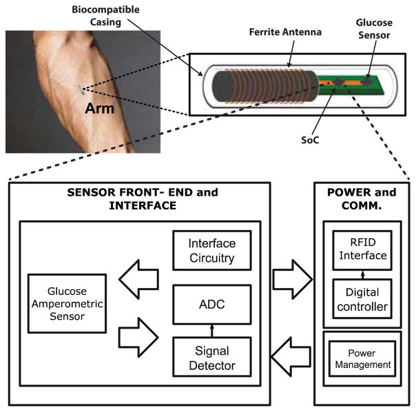
This work presents an integrated system-on-chip (SoC) that forms the core of a long-term, fully implantable, battery assisted, passive continuous glucose monitor (Fig. 1). It uses a 13.56 MHz, Industrial Scientific and Medical band (ISM) RF signal to harvest energy and communicate data to an interrogating reader. Harvested energy is stored in an off chip printable battery for use in absence of the RF field. The monitor includes an off-chip amperometric electrochemical glucose sensor, ferrite antenna, printable battery, and SoC. Section II describes the proposed architecture whereas implementation is provided in section III. Transistor level simulations are presented in section IV, and finally conclusions in section V.
Fig. 1.
Wireless powered implantable sensor tag for continuous glucose monitoring.
II. SYSTEM LEVEL ARCHITECTURE
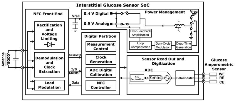
Fig. 2 illustrates the System level architecture of the SoC. Sensor read out and digitization includes a potentiostat that interfaces directly with the glucose sensor leads and conditions the readout signal for digitization by the frequency discriminator based analog to digital converter (ADC). During wireless transmission, two coupled coils are used, the reader’s coil and the SoC connected ferrite antenna. NFC front end rectifies harvested RF energy providing an unregulated supply (Vrec) to the power management unit. It is also responsible for communication with the reader via load modulation. Power management unit generates two regulated, 0.4V (digital) and 0.9V (analog) supplies. When an interrogating field is present, Vrec is supplied by rectification circuitry. The regulated digital output powers the digital core and recharges the off-chip battery and on-chip storage capacitor. Once the RF field is removed, Vrec is supplied by the battery and storage cap. The digital partition includes control and calibration circuits, decodes incoming commands and manages system operation.
Fig. 2.
System level architecture for the interstitial glucose monitor SoC.
III. IMPLEMENTATION
A. Amperometric Sensor Front-End and ADC
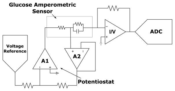
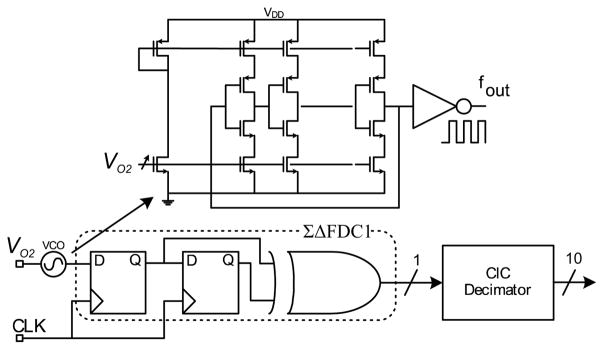
The amperometric sensor used has an active area of 0.1 mm2 and sensitivity of 0.05 μA·mm−2 · mM−1 for clinically relevant glucose concentrations (0 – 30 mM). It has three electrodes, working, reference, and counter electrodes (WE, RE, and CE, respectively, Fig. 3). When a constant voltage is applied between (WE) and (RE) (250 mV in this work) by the potentiostat, a current proportional to interstitial glucose concentration is produced. For RE to ideally draw zero current and track the applied voltage, the amplifiers A1 and A2 require large gain. This is achieved using folded cascaded topology with device stacking and rail-to-rail input/output stages to drive the large double layer capacitor of CE and WE. The output current is converted to voltage via the I-to-V converter. The front-end can resolve a current range of 1 nA to 1μA with an Integrated input referred noise voltage of 20 μVrms in the measurement band of 1 – 25 Hz. Input referred DC offset is 1.6 nV. A 1st order, digital, none feedback, ΣΔ frequency Discriminator (ΣΔFDC) is used to implement the ADC [4]. It processes a frequency modulated (FM) input signal to produce a single bit output stream. A schematic of the ΣΔFDC is shown in Fig. 4. It consists of a voltage controlled oscillator (VCO), two D flip flops and one XOR gate. Decimation of ΣΔFDC output is implemented using CIC filter to generate a 10 bit code word.
Fig. 3.
Analog front-end for the glucose sensor.
Fig. 4.
ΣΔ based frequency discriminator analog-to-digital converter.
B. Power Management
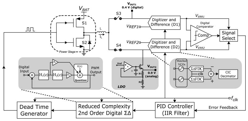
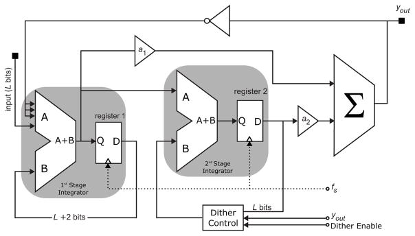
Fig. 5 illustrates the proposed power management unit used in this work. It is a switched mode single inductor, dual output regulator. Two error signals VERR1 and VERR2 are generated from the regulated output voltages VOUT1 (digital) and VOUT2 (analog) respectively [5]. The signals VERR1 and VERR2 are compared using the comparator (Comp). The higher of the two signals is then passed through the ‘signal select’ block to the PID controller. Instead of using a conventional pulse width (PWM) or pulse code (PCM) modulator to drive the power stage, a 2nd order ΣΔ modulator (Fig. 6) is used to avoid tonal noise. The comparator’s decision controls the operation of switches S3 and S4. If VERR1 > VERR2, then S3 is closed and S4 is left open and vice versa. This arrangement allows the control loop to regulate the two output voltages by tracking the signals VERR1 and VERR2 and adjusting the on/off times for S3 and S4. Digital implementation of the loop controller allows for low power consumption, ease of programmability, and high tolerance to mismatch and process variations. Blocks D1 and D2 digitize the output voltages VOUT1 and VOUT2 using 1st order ΣΔFDCs similar to the one used to digitize the sensor’s output. To generate the error signals VERR1 and VERR2, the digital representation of VOUT1 and VOUT2 is subtracted from the digitized reference voltages VREF1 and VREF2 respectively. To reduce the switching ripple generated by the regulator and generate a stable analog supply for the amperometric sensor, an LDO is used in series with the VOUT2. This arrangement allows for maximum power efficiency and very low supply line ripple needed for accurate reference generation and sensor readout. Inductor (L) is realized using on chip top metal spiral windings.
Fig. 5.
System level architecture for the power management unit.
Fig. 6.
2nd order digital ΣΔ modulator implementation.
C. NFC Front End
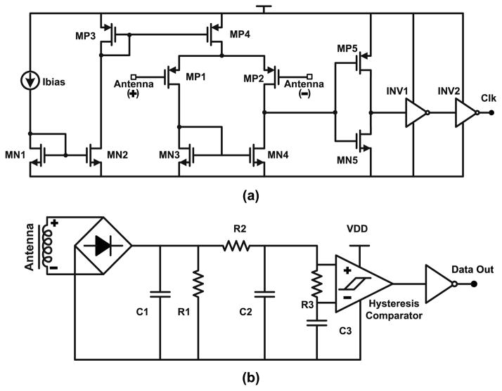
An ASK demodulation circuit (Fig. 7b) composed of a rectifier, diode based envelope detector, low pass filter and comparator with an average signal driven threshold is used to read the interrogator’s commands. Fig. 7a shows the clock extraction circuit used to extract a 13.56-MHz clock from the carrier. It is composed of a high bandwidth differential comparator followed by inverters. Extracted clock is used to generate remaining system clocks in the digital partition. A 40mV minimum antenna output signal is needed to for successful extraction. Load shift key (LSK) is used to generate remaining system clocks in the digital partition. A 40mV minimum antenna output signal is needed to for successful extraction. Load shift key (LSK) is used to transmit data back to the reader by varying the load impedance of the passive wireless link.
Fig. 7.
Schematic diagrams of the (a) clock extractor and (b) demodulation circuits.
IV. Simulation Results
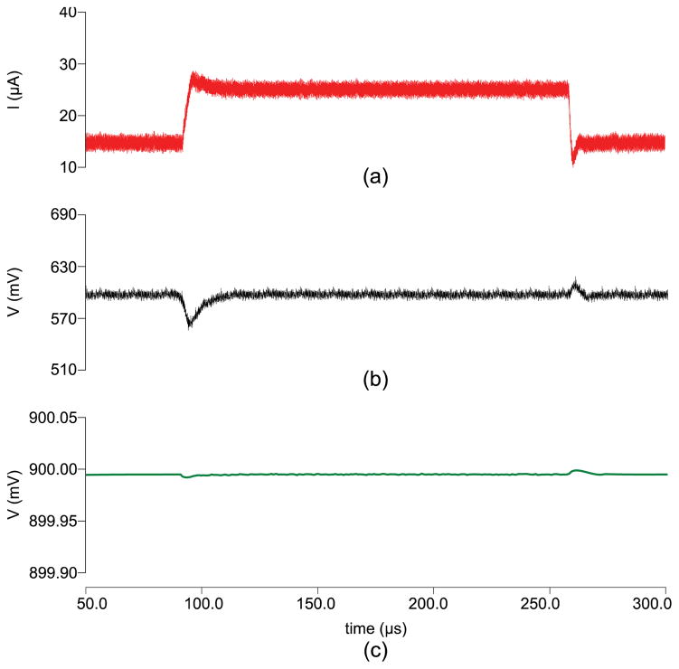
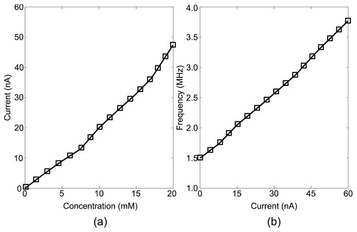
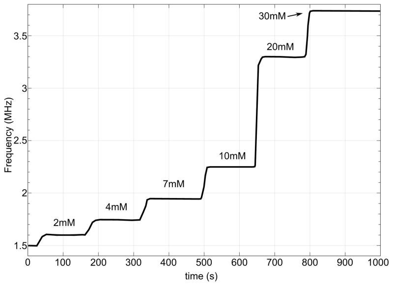
The SoC was designed in 14nm bulk CMOS process and validated through simulations. Target specifications for the integrated power management unit are a total output current of 1 mA while charging the battery and operating the sensor and NFC front ends simultaneously, down to 15 μA while running off battery power alone. Output switching ripple must remain below 20 mV and 10 μV for digital and analog regulated supplies respectively. Fig. 8 demonstrates load regulation test in presence of the RF field. The two output voltages, Vout1 and Vout2, are regulated to 0.4 V and 0.9 V respectively. At t = 100μs, Total output current (IL) is ramped up from 15 μA to 28 μA and back down at t = 250μs, both outputs settle back to nominal values in 12 μs. Fig. 9a demonstrates the measured sensor only transfer characteristics and simulated post layout VCO sensitivity. The simulated results of a continuous glucose flow test are shown in Fig. 10. The SoC layout is provided in Fig. 11. Key metrics are summarized in Table 1.
Fig. 8.
Power regulation during charging operation showing (a) total output current, (b) regulated digital output (VOUT1) and (c) regulated analog output (VOUT2). Charging engaged at t = 100μs and disengaged at t = 250μs.
Fig. 9.
(a) Measured sensor current versus glucose concentration and (b) simulated VCO frequency versus sensor output current.
Fig. 10.
Post layout transient simulation response of the continuous glucose monitor running on battery power (RF rectification disengaged). Glucose concentration 0mM.at t = 0s.
Fig. 11.
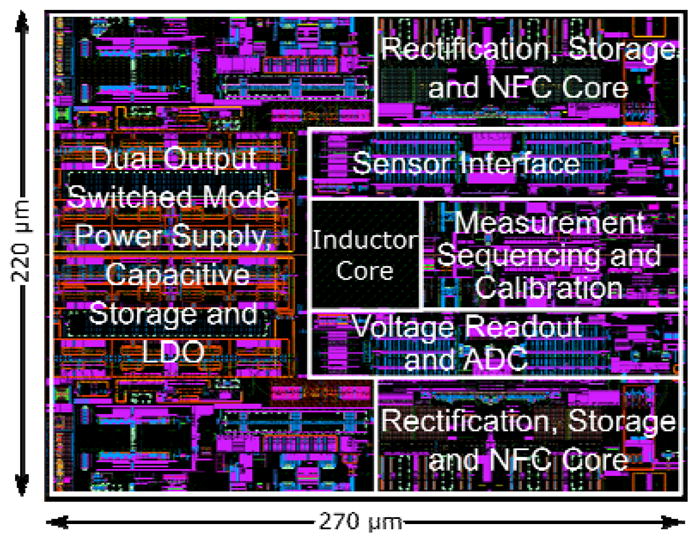
Layout of the glucose monitor SoC showing base layers only. Inductor windings on top metal layers are not visible.
Table 1.
Key System Metrics
| Unregulated Supply Voltage Range (V) | 1.0 – 3.3 |
| On-Chip Inductor (nH) | 20 |
| Efficiency, Rectifier, Regulator (%) | 46, 94 |
| Total Power Consumption (W) | Charging Enabled: 47m Charging Disabled: 24μ - Potentiostat: 2.5μ - ΣΔFDC: 50n - NFC Front-End: 12μ - Digital Controller:110n - SMPS (Loop Controller): 9μ |
V. Conclusion
This work presented an integrated system-on-chip (SoC) that forms the core of a long-term, fully implantable, battery assisted, passive continuous glucose monitor. It integrates an amperometric glucose sensor interface, a near field communication (NFC) wireless front-end and a fully digital switched mode power management unit for supply regulation and on board battery charging. It uses 13.56 MHz (ISM) band to harvest energy and backscatter data to an NFC reader. System was implemented in 14nm CMOS technology and validated with post layout simulations.
Contributor Information
Nijad Anabtawi, Intel Corporation, Chandler, AZ and the Department of Electrical Engineering, Arizona State University, Tempe, AZ.
Sabrina Freeman, Department of Biomedical Engineering, Arizona State University, Tempe, AZ.
Rony Ferzli, Department of Electrical Engineering, Arizona State University, Tempe, AZ.
References
- 1.International diabetic federation. 2014 Dec; [Online]. Available: http://www.idf.org/
- 2.Dehennis A, et al. An NFC enabled CMOS IC for a Wireless, Fully Implantable Glucose Sensor. Biomedical and Health Informatics, IEEE Journal of. PP(99):1–1. doi: 10.1109/JBHI.2015.2475236. [DOI] [PubMed] [Google Scholar]
- 3.Ricci F, et al. Ex vivo continuous glucose monitoring with microdialysis technique: The example of glucoday. IEEE Sens J. 2008 Jan;8(1):63–70. [Google Scholar]
- 4.Wismar, et al. A 0.2V, 7.5 μW, 20 kHz ΣΔ modulator with 69 dB SNR in 90 nm CMOS. Solid State Circuits Conference, 2007. ESSCIRC 2007. 33rd European; Sept. 2007. [Google Scholar]
- 5.Anabtawi N, Ferzli R. A simplified single-inductor dual-output DC-DC buck converter architecture with a fully digital Σ-Δ based controller. Quality Electronic Design (ISQED), 2015 16th International Symposium on; 2–4 March 2015.pp. 82–85. [Google Scholar]


