

Abstract
Photon counting arrays (PCAs), defined as pixelated imagers which measure the absorbed energy of x-ray photons individually and record this information digitally, are of increasing clinical interest. A number of PCA prototypes with a 1 mm pixel-to-pixel pitch have recently been fabricated with polycrystalline silicon (poly-Si) — a thin-film technology capable of creating monolithic imagers of a size commensurate with human anatomy. In this study, analog and digital simulation frameworks were developed to provide insight into the influence of individual poly-Si transistors on pixel circuit performance — information that is not readily available through empirical means. The simulation frameworks were used to characterize the circuit designs employed in the prototypes. The analog framework, which determines the noise produced by individual transistors, was used to estimate energy resolution, as well as to identify which transistors contribute the most noise. The digital framework, which analyzes how well circuits function in the presence of significant variations in transistor properties, was used to estimate how fast a circuit can produce an output (referred to as output count rate). In addition, an algorithm was developed and used to estimate the minimum pixel pitch that could be achieved for the pixel circuits of the current prototypes. The simulation frameworks predict that the analog component of the PCA prototypes could have energy resolution as low as 8.9% FWHM at 70 keV; and the digital components should work well even in the presence of significant TFT variations, with the fastest component having output count rates as high as 3 MHz. Finally, based on conceivable improvements in the underlying fabrication process, the algorithm predicts that the 1 mm pitch of the current PCA prototypes could be reduced significantly, potentially to between ~240 and 290 μm.
Keywords: photon counting arrays, photon counting pixel circuits, polycrystalline silicon thin-film transistors, circuit simulations, medical x-ray imaging
I. Introduction
Photon counting detectors (PCDs), which measure the absorbed energy of x-ray photons individually and record this information digitally, are of increasing clinical interest for x-ray imaging. Compared to conventional fluence detectors that integrate absorbed energy information over an entire image frame, PCDs offer many advantages such as improving image quality through reduction of Swank noise and electronic noise, and providing inherent spectral information by means of multiple energy discriminating windows. Such devices are presently in clinical use for mammographic imaging (Lundqvist et al., 2003) and are under development for breast tomosynthesis (Fredenberg et al., 2009). PCDs are also being explored for other imaging modalities such as computed tomography (Shikhaliev and Fritz, 2011; Taguchi and Iwanczyk, 2013; Schlomka et al., 2008).
While those PCDs used in breast imaging applications employ a scanned-slit detector arrangement, the development of imagers consisting of large-area, two-dimensional arrays of photon counting pixels would enable radiographic and fluoroscopic imaging without the motion artifact problems associated with scanning. A number of 2D, pixelated photon counting arrays (PCAs) based on crystalline silicon (c-Si) have been reported (Campbell et al., 1998; Fischer et al., 2000; Locker et al., 2004; Perenzoni et al., 2008; Llopart et al., 2002; Ballabriga et al., 2011). These prototype devices have detection areas up to ~1.5×1.5 cm2 with pixel pitches ranging from 55 μm to 350 μm and employ in-pixel circuits that allow up to 8 energy windows. Such detection areas are insufficient for general radiography and fluoroscopy applications, and while these devices could, in principle, be tiled in order to achieve larger detection areas, such tiling would likely result in loss of sensitivity at the tile boundaries as well as present engineering challenges. For these reasons, the development of imagers based on large-area, monolithic PCAs, which would eliminate the need for tiling, would be desirable, but the fabrication processes used to create c-Si circuits are generally not well-suited for economic manufacture of such large-area devices.
One interesting approach capable of overcoming this limitation involves the technologies of large-area, thin-film electronics. An early incarnation of these technologies, based on hydrogenated amorphous silicon (a-Si:H), was used to create the first active matrix, flat-panel imagers (AMFPIs) in the late 1980s. AMFPIs are now widely employed in clinical settings and have detection areas as large as ~43×43 cm2. However, the low electron and hole mobilities of a-Si:H (~1 and 10−2 cm2/Vs, respectively) are insufficient for the type of circuits required for a clinical PCA imager. In particular, circuits created using thin-film transistors (TFTs) based on a-Si:H would have slow switching speeds, which would severely restrict the maximum photon counting rates of arrays utilizing this material. In addition, the hole mobility of a-Si:H is insufficient for the creation of useful p-type TFTs, precluding creation of the complimentary-logic circuits which are typically necessary for photon counting circuits. However, further advances in thin-film technology have led to the development and use of TFTs based on low-temperature polycrystalline silicon (poly-Si) in a variety of commercial devices, such as displays for monitors and mobile phones. Poly-Si offers electron and hole mobilities approximately two and four orders of magnitude greater, respectively, than those of a-Si:H, overcoming many of the disadvantages of that material. In addition, poly-Si transistors have demonstrated good radiation tolerance (Li et al., 2006). Prototype active pixel imagers incorporating in-pixel amplification based on poly-Si TFTs have demonstrated over an order of magnitude increase in signal, as well as the ability to perform advanced readout techniques (El-Mohri et al., 2009). Such techniques allow significantly improved signal-to-noise ratio performance compared to that of conventional a-Si:H-based AMFPIs. Given these encouraging results, poly-Si appears to be a promising and suitable candidate material for creation of photon counting circuits.
Recently, the first prototype PCAs based on poly-Si TFTs, which include 11 separate pixel designs collectively referred to as SPC1, have been developed toward the long-term goal of creating large-area, monolithic devices (Liang et al., 2014). In parallel, simulation frameworks and mathematical models have been developed to provide insight into the signal and noise behavior of individual poly-Si TFTs within the photon counting circuits, as well as the impact of variations in TFT performance on overall photon counting performance — information that is not obtainable empirically from prototypes. In the present study, results from simulations and models pertaining to the circuit components used in the SPC1 array pixels are reported.
II. Methods
The SPC1 prototype arrays have an 8×8 pixel format and a 1 mm pitch. Each pixel has four main components: an amplifier, a comparator, a clock generator, and a counter, as shown in Fig. 1. For each component, a variety of different circuit designs were created: 3 amplifier designs, 2 comparator designs, 4 clock generator designs, and 3 counter designs. Each of the 11 SPC1 array designs incorporate a pixel type corresponding to some combination of designs for these four main components.(Liang et al., 2014) The first component, the amplifier, magnifies an input signal, after which the comparator circuit outputs a digital “high” if the input exceeds a user-defined threshold level. If the comparator output is high, the signal is converted by the clock generator into a two-phase clock (i.e., two separate signals with non-overlapping pulses), which is then used to increment the counter. As shown in Fig. 1, the components can be classified as analog or digital depending on the type of signal present at the input and output of the component, with the comparator component regarded as both since it has an analog input and a digital output. For this study, the comparator component is considered to be solely in the digital domain.
Figure 1.

Diagram of the four main circuit components of the prototype photon counting pixels: an amplifier, a comparator, a clock generator, and a counter. The waveforms between components schematically illustrate the shape of the signals at that point in the design. The clock generator component has two outputs, denoted by black and grey lines.
Two simulation frameworks, an analog framework for simulation of analog components and a digital framework for simulation of digital components, were developed to estimate the performance of each circuit design. These frameworks, implemented using the Eldo SPICE circuit simulator software package (Mentor Graphics, OR), were used to examine intrinsic noise, robustness, and output count rate, and are described in the following sections.
In addition to simulating analog and digital performance, a study was conducted to estimate the impact of anticipated advances in processing technology on the pixel pitch of future hypothetical prototypes. To that end, an algorithm was developed to estimate the minimum possible pixel pitch of the current prototype designs as a function of minimum feature size and 3D spatial organization of the circuits.
IIa. Methods — Transistor parameters and noise characteristics
Both simulation frameworks employ version 2 of the RPI poly-Si TFT model (Iniguez et al., 1999) for modeling transistor behavior. In order to make the simulations representative of the low-temperature poly-Si material under consideration, transistor model parameter values, including mobility (μ00) and threshold voltage (Vt0), were extracted from transfer and output characteristics measured from individual poly-Si TFTs. (Transfer and output characteristics were obtained by measuring channel current as a function of gate voltage and drain-source voltage, respectively.) A set of such parameter values obtained from a single transistor is called a “model card”. The transfer and output characteristics obtained from different poly-Si TFTs are not as tightly uniform as those of c-Si transistors, largely due to variations in the dimensions of the crystal grains that are formed during laser-annealing of amorphous silicon to create poly-Si on quartz substrates,(Boyce et al., 2001) as well as variations in unintended channel doping. In particular, such non-uniformity in signal characteristics can be considerable from substrate to substrate and, though more subdued, still non-negligible across a given substrate. In order to examine the effects of such non-uniformity, model cards derived from transistors across many different substrates were used in the digital framework to simulate variations caused by the fabrication process. By comparison, for the case of the analog framework, uniform transistor characteristics were assumed. This involved choosing one n-type transistor and one p-type transistor with favorable values for μ00 and Vt0 as “standard” transistors. The model cards corresponding to these standard transistors were used in the analog framework to simulate the signal and noise performance of amplifier circuits.
TFT noise characteristics were also measured for use in the analog framework. These were obtained by measuring the variations in the channel currents of the standard transistors (sampled at ~4 Hz for 1 hour) for different combinations of drain, source, and gate bias values. At such low frequencies, these variations are mainly due to flicker noise. The channel current variations were then referred to the gate (as voltage variations), converted into a noise power spectral density (using a Fourier transform) and were fit using the following model equation for flicker noise (Razavi, 2002; Tsividis and McAndrew, 2011):
| [1] |
In this equation, SV(f) is the noise power spectral density, referred to the gate; kf is the process-dependent flicker noise constant of the transistor; Cox is the gate oxide capacitance (set to 0.345 fF/μm2 for the devices considered in this study — a value which was derived from processing parameters and material properties); W and L are the width and length, respectively, of the gates of the measured transistor; and f is frequency in Hz. Fits of Eq. 1 to the measured SV(f) spectra were used to determine kf values. Since the standard model cards were used to simulate every transistor in the amplifier designs, and since each transistor is operated at different gate, drain, and source voltages, channel current for each standard transistor was measured at gate, drain, and source voltage values representative of the range of operating conditions for the amplifier designs. The averages of the kf values obtained over these operating conditions (referred to as kfn and kfp for the n-type and p-type standard transistors, respectively) were used as parameters to model the noise characteristic of the transistors.
IIb. Methods — Amplifier performance simulations
The analog simulation framework was developed to investigate the amount of intrinsic noise in the amplifier component of the SPC1 arrays. Intrinsic noise refers to the noise generated by the transistors in the circuit — which can affect image quality. This noise was quantified in terms of the ratio of signal to noise (SNR).
In this study, the signal portion of the SNR was chosen to be the maximum change in the output voltage of the amplifier in response to an ~2.44 fC charge injection to an input capacitor — simulated in the frequency domain, from 0.1 Hz to 10 MHz. This injection of charge corresponds to a 70 keV photon interacting with a cadmium zinc telluride (CZT) detector with a work function (i.e., the average amount of energy required to produce an electron-hole pair) of 4.6 eV (Limousin, 2003). The input capacitor was assumed to be 1×1 mm2 with a 500 μm thick (Tokuda et al., 2001) dielectric (consisting of CZT) having a relative permittivity of 10. The gain of the amplifier can vary, as discussed below, but a signal magnitude between 1.25 and 2 V (a range expected to be sufficient to allow good comparator performance) was desired.
The noise portion of SNR was taken to be the intrinsic noise of the amplifier, which was computed as follows. For a given transistor in the circuit design, Eq. 1 was used to determine SV from 0.1 Hz to 10 MHz using the average kf value derived from the appropriate standard transistor (i.e., kfp or kfn), as well as the W and L for that transistor. (Note that outside of this frequency range, all transistors were found to have negligible effect on the intrinsic noise of the amplifier.) In order to account for the frequency-dependent gain applied to SV, the frequency response of the output of the amplifier was determined by applying a small, 1 mV AC input at the gate of that transistor and performing a simulation in the frequency domain, again from 0.1 Hz to 10 MHz. From the simulation results, gain at each frequency was determined by dividing the AC output voltage magnitude of the amplifier by the AC input voltage magnitude. The SV value at each frequency was weighted with the appropriate gain value, and this weighted SV curve was integrated over the frequency range. The resulting “transistor noise value” (in units of volts) is the noise contribution of that transistor to the overall amplifier output. This procedure was repeated for every transistor in each amplifier design. The sum in quadrature of the noise values for all the transistors in a design represents the total intrinsic noise (also in units of volts) of that design.
Two amplifier designs were considered in this study. Both designs are 3-stage, folded cascode circuits. The circuit diagrams for the two designs (a 3-stage, 1st order bandpass filter and a 3-stage, 2nd order bandpass filter) are shown in Figs. 2a and 2b, respectively. The amplifier input was simulated using the circuit shown in Fig. 2c and consists of a current source providing the ~2.44 fC input to the capacitor formed by the CZT detector which is in parallel with a 100 MΩ resistor to ground. The circuit diagram for a single folded cascode circuit is shown in Fig. 2d. The voltage bias inputs VAGC, VB, and VCG are used to control the gain and the cutoff frequencies of the amplifier.
Figure 2.
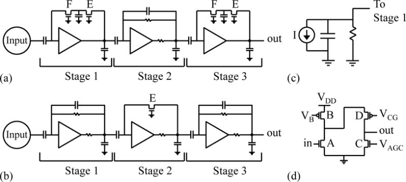
Circuit diagrams for the amplifier designs considered in this study: (a) a 3-stage, 1st order bandpass filter design, and (b) a 3-stage, 2nd order bandpass filter design. In these figures: the circles labeled “Input” represent the circuit shown in (c); the triangles are folded cascode circuits, the diagram of which is shown in (d); and the stages are labeled as Stage 1, Stage 2, and Stage 3. Transistors in the folded cascode circuit are labeled A through D, and transistors not related to the folded cascode circuit are labeled E and F.
To determine the most suitable set of voltage bias input values, the analog framework was used to simulate the circuit at various voltage levels for each bias value. VAGC and VB were varied from 0 to 6 V in 0.1 V steps and 0.25 V steps, respectively. VCG has only a minor effect on gain or bandwidth and was fixed at 0.25 V. VDD, the power rail for the circuit (a notation used for all circuits considered in the study), was fixed at 8 V. An SNR value was calculated for each combination of bias settings and the combination resulting in the highest SNR, while also providing the desired output voltage (i.e., between 1.25 and 2 V), was identified as the best combination. For a given amplifier design, once the best combination was determined, the equivalent input noise of that design (Enoise) in units of energy was calculated by dividing the input photon energy Ein (i.e., 70 keV) by the resulting SNR value. For each amplifier design, the energy resolution (ΔE), in terms of the full width at half maximum (FWHM) and expressed as a percentage of the input photon energy, was determined as follows:
| [2] |
IIc. Methods — Comparators clock generator performance simulations
The digital simulation framework was developed to evaluate the performance of the various circuit designs of the digital components, taking into account the effects of non-uniformity in poly-Si TFT signal characteristics caused by the fabrication process (as discussed in Sec. IIa). To investigate the effect of such non-uniformity, simulations were performed on circuits that had randomly chosen model cards assigned to every transistor. A circuit with model cards assigned in this way is referred to as a “variation.” For each digital component, numerous variations were created for each design for the purpose of scoring and ranking the designs by their “robustness” — defined as the percentage of variations meeting certain select criteria (detailed in Sees. IIIc and IIId). Circuits with higher scores are expected to exhibit superior ability to meet the criteria — thereby reflecting better tolerance to TFT non-uniformities.
The comparator and clock generator components were simulated together to take into account their interdependencies. The four combinations of comparator+clock generator components employed in the SPC1 prototype arrays are summarized in Table 1 and all those combinations were examined in the study. For each combination, a total of 200 variations were created. The circuit diagrams of the two comparator designs are shown in Fig. 3. In the figure, VB1 is a bias input and VT is the threshold voltage level. The circuit diagrams for the four clock generator designs are shown in Fig. 4, with the two configurations of the 5-inverter design (referred to as long-delay and short-delay in Table I) represented by the circuit diagram in Fig. 4a.
Table 1.
Combinations of comparator and clock generator designs examined in the study. Each design pair is employed in the corresponding SPC1 arrays (described in more detail in reference Liang et al., 2014) indicated in the last column.
| Design ID | Comparator design | Clock generator design | Used in SPC1 Array |
|---|---|---|---|
| 5inv-long | Schmitt trigger | 1 SR + 5-inverter (long-delay) | Pxl2, Pxl3 |
| 5inv-short | Differential pair | 1 SR + 5-inverter (short-delay) | Pxl4 |
| 7inv | Differential pair | 1 SR + 7-inverter | Pxl6 |
| 3inv-2SR | Differential pair | 2 SR + 3-inverter | Pxl5, Pxl7, Pxl8, Pxl9 |
Figure 3.
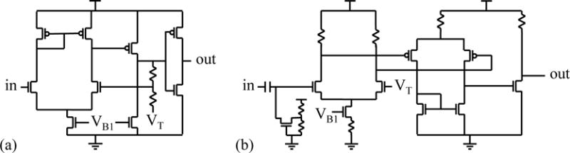
Circuit diagrams for the comparator designs considered in this study: (a) a Schmitt trigger design, and (b) a differential pair design. For both designs, two adjustable inputs, VB1 (bias) and VT (threshold), are labeled.
Figure 4.
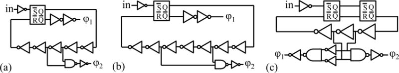
Circuit diagrams for the clock generator designs considered in this study: (a) a 5-inverter design (corresponding to two configurations: long-delay and short-delay), (b) a 7-inverter design, and (c) a 2-SR latch design. In the diagram, the rectangles represent 2-NAND-gate-based SR (i.e., set-reset) latches; the combined triangle-and-bubble symbols represent inverter stages; and the combined plug-shape-and-bubble symbols represent NAND gates. The outputs of the clock generator are denoted as φı and φ2.
For the simulation of the variations of these four combinations, the input consisted of a train of square input pulses parameterized by a variable, tmin. For each variation, a three-dimensional sweep of VB1 and VT voltage levels, and tmin time values was simulated to investigate the performance of that variation over a wide range of operating conditions. The VB1 levels ranged from 0 to 6 V in 0.5 V steps; the VT levels ranged from 3 to 5 V in 1 V steps; and tmin had values of 10, 32, 100, 316, 1000, 3162, and 10000 ns — which, with 200 variations, resulted in a total of 54,600 simulations for each combination. For each of the 7 values of tmin the width of each pulse and the time between pulses was assigned a random multiple of that value — resulting in 7 different input pulse trains.
IId. Methods — Counter performance simulations
The counter architecture implemented in the SPC1 prototype arrays is a 9-bit, maximum-length linear feedback shift register (LFSR) operated by a two-phase clock. This LFSR is a pseudorandom counter with 511 unique states. A two-phase clock “cycle” is used to increment the counter by one step. After advancing 511 steps from a given starting point, the counter “loops” back to that starting value. Three different counter designs were implemented in the SPC1 prototype arrays and a schematic circuit diagram of one bit of each design is shown in Fig. 5.
Figure 5.
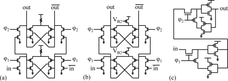
Circuit diagrams for one bit of each of the counter designs considered in this study: (a) a differential-pair with resistive load design (referred to as Differential-Res), (b) a differential-pair with transistor load design (referred to as Differential-TFT), and (c) a gated-bit design. The symbols φı and φ2 indicate inputs provided by the preceding clock generator component. The bias voltage VB2 was set to 4 V.
The counter component was also evaluated with the digital framework. Similar to the comparator+clock generator simulations, 200 variations of each counter design were simulated. Unlike the comparator+clock generator simulations which had 3 input variables, the counter simulations only had a single dependency: the two-phase clock. Thus, all variations of the counter component were evaluated by changing the timing of this clock.
Each variation was simulated for a minimum of 511 clock cycles, corresponding to at least one full loop of the counter. Each two-phase clock cycle consisted of non-overlapping clock pulses on two different inputs, labeled as φı and φ2 in Fig. 5. For example, for a given clock cycle duration of 1000 ns (corresponding to a count rate of 1 MHz), φı will be high for 375 ns, then it will be low for the remaining 625 ns; φ2 will be low for the first 500 ns, then high for 375 ns, then low for the remaining 125 ns. Count rates of 0.1, 0.25, 0.5, 1, 2, and 3 MHz were simulated.
IIe. Methods — Minimum pixel pitch calculations
The SPC1 prototype arrays were designed and fabricated using a minimum feature size of 6 μm, which defines the smallest transistor gate dimension allowed in the design. The fabrication process employed 4 metal layers, a-Si:H-based resistors, and a 100 nm thick SiO2 gate dielectric that was also used to form capacitors. The pixels are arranged in a quad format with a group of 4 pixels sharing common wires (e.g., bias and power lines). To facilitate common wire routing to peripheral electronic pads, a 1 mm pixel pitch was employed for all SPC1 arrays, resulting in the layouts of the circuits of each design not fully utilizing the 1 mm2 pixel area.
In order to estimate the minimum pitch achievable for a given SPC1 array design, an algorithm was developed to calculate the area occupied by circuit elements such as transistors, resistors, and capacitors in each component, as well as the area occupied by the common wires. In the algorithm, the occupied area for each transistor is estimated to be 9 times the gate area (defined as the product of W and L) of that transistor in order to account for source and drain contacts, as well as for spacing between other elements. Next, the area occupied by capacitors and resistors is multiplied by 2 and 3, respectively, to account for spacing between other elements. The larger factor of increase used for resistors compared to that used for capacitors is due to consideration of the oblong shape of resistors (which increases the perimeter of the element) as opposed to the more square-like layout of the capacitors employed in the designs. Finally, the area occupied by common wires (which is estimated to be 0.25 mm2 for the SPC1 designs) was assumed to be dependent on the number of metal layers but independent of minimum feature size. The minimum pixel pitch is given by the square root of the total circuit area (corresponding to the sum of the areas of the transistors, capacitors, resistors, and common wires) computed by the algorithm.
Two pixel designs were considered — one with the largest component area (corresponding to Pxl3) and one with the smallest component area (corresponding to Pxl5). Microphotographs corresponding to each design are shown in Fig. 6. A decrease in pixel pitch was explored by employing three strategies: eliminating unoccupied pixel area, reducing the minimum feature size, and increasing the number of metal layers used in the fabrication process. Eliminating unoccupied pixel area involved excluding areas where no circuits were fabricated from the overall pixel pitch determination. Reducing minimum feature size, which is assumed to only affect the area occupied by transistors and resistors, involved shrinking that design rule from 6 μm down to 3 μm and then to 1 μm. However, instead of assuming a quadratic decrease in occupied area (which would be the consequence of reducing, for example, both the width and length of the transistors), a linear reduction was assumed to approximately account for non-shrinking elements, such as inter-layer contacts (i.e., vias), and source and drain contacts for the TFTs. Finally, 4 additional metal layers were introduced in the fabrication process to allow the area required for the common wires to be distributed over more planes.
Figure 6.
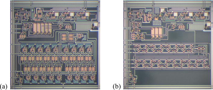
Microphotographs of a single pixel from (a) the Pxl3 array with 229 transistors, 9 capacitors, and 26 resistors and (b) the Pxl5 array with 197 transistors, 11 capacitors, and 12 resistors.
III. Results
IIIa. Results — Transistor parameters and noise characteristics
Transfer and output characteristics were measured from approximately 320 individual poly-Si transistors sampled from 20 substrates. From that data set, a total of 16 transistors (8 n-type and 8 p-type) with threshold voltages approximately equally spaced between −0.3 and 1 V (for n-type) or 0 and −1 V (for p-type) were selected. Transfer characteristics from these transistors are plotted in Fig. 7, after normalization by the W-to-L ratio of each transistor.(Razavi, 2002) The spread observed in the data illustrates the effect of process variations during fabrication (e.g., due to laser-annealing or doping).
Figure 7.
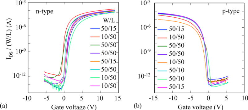
Normalized transfer characteristics measured from (a) 8 n-type and (b) 8 p-type poly-Si TFTs. The legend indicates the dimensions of W and L, in μm, for the individual transistors.
From the unnormalized transistor measurement results, a total of 16 model cards were created. For these cards, the minimum and maximum values of mobility and threshold voltage are summarized in Table 2 — along with the corresponding values for the standard n-type and p-type transistors. Separately, from noise power spectra obtained from channel current measurements, the average values for kf in Eq. 1 for the n-type and p-type transistors, kfn and kfp, were determined to be 4.5×10⁻²⁵ and 7.6×10⁻²⁵ C2/m2, respectively.
Table 2.
Minimum and maximum mobility (μ00) and threshold voltage (Vt0) values for the 8 n-type and 8 p-type transistor model cards. The values for the standard transistor model cards are also shown.
| Parameter | n-type | p-type | ||||
|---|---|---|---|---|---|---|
| min | standard | max | min | standard | max | |
| μ00 (cm2/Vs) | 89.2 | 134.5 | 178.6 | 46.5 | 78.1 | 78.4 |
| Vt0 (V) | −0.26 | 0.35 | 0.96 | −0.80 | −0.47 | −0.19 |
IIIb. Results — Amplifier performance simulations
Figure 8 shows the simulation results for output signal, intrinsic noise, and SNR as a function of VAGC and VB for the two amplifier designs considered in the study. Figures 8a and 8d show that there are regions where amplifier output signal increases quickly, as illustrated by the sharp transition between the blue and the dark-red regions. Figures 8b and 8e show that intrinsic noise is highest when the corresponding output signal is highest. Finally, Figs. 8c and 8f indicate that the SNR is highest where output signal is only moderately high.
Figure 8.
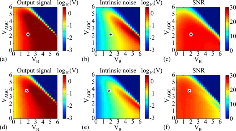
Results for (a) output signal, (b) intrinsic noise, and (c) SNR for the 3-stage, 1st order bandpass amplifier plotted as a function of VAGC and VB – with the best combination indicated by the superimposed “plus” symbol, (d), (e), and (f) show the corresponding signal, noise, and SNR results for the 3-stage, 2nd order bandpass amplifier – with the best combination indicated by the “cross” symbol. For each plot, the color bar to the right denotes the scale. Note that output signal and intrinsic noise are plotted on a logarithmic scale while SNR is plotted on a linear scale.
In Fig. 8, the “plus” and “cross” symbols superimposed upon the plots denote the best combination of VAGC and VB bias settings — i.e., the one that provides the highest SNR, while also providing the desired output signal (i.e., between 1.25 and 2 V). That best combination for the 3-stage, 1st order bandpass design and the 3-stage, 2ND order bandpass design is (VAGC=2.3 V, VB=2.00 V) and (VAGC=3.9 V, VB=1.75 V), respectively.
For each amplifier design at its best combination of bias settings, transistor noise values for each TFT (referred to the output of the amplifier) are given in Fig. 9. From the figure, for each stage of each design, transistors A and B are seen to contribute more noise than the other transistors. Furthermore, transistors in the earlier stages generally contribute greater noise than their counterparts in later stages — a consequence of the noise being magnified through the remainder of the amplifier chain.
Figure 9.

Noise values, referred to the output of the amplifier, for each transistor in the 3-stage, 1st order bandpass and 3-stage, 2nd order bandpass amplifier designs, indicated by the black and grey bars, respectively. The transistor results are grouped by stage. In each stage, the letters A through F correspond to the transistors appearing in Fig. 2. Finally, the use of the notation “NA” in place of a black or grey bar indicates the absence of that transistor in a given stage of a design.
Table 3 summarizes the simulation results for the two amplifier designs operated at their respective best combination of bias settings. For the 3-stage, 1st order bandpass design, the output signal was 1.99 V and the total intrinsic noise was 75.1 mV, which corresponds to an SNR of 26.5. For this design, the equivalent noise of the design in units of energy was 2.64 keV — resulting in an energy resolution of 8.9% FWHM at 70 keV. For the 3-stage, 2nd order bandpass design, the output signal was 1.29 V, and the intrinsic noise was 52.5 mV, which corresponds to an SNR of 24.6. For this design, the equivalent noise was 2.85 keV — resulting in an energy resolution of 9.6% FWHM at 70 keV. The energy resolution of the SPC1 amplifier designs is comparable to those reported for c-Si PCAs. (Fredenberg et al., 2010; Barber et al., 2009)
Table 3.
Simulation results for output signal, total intrinsic noise, SNR, equivalent noise, and energy resolution corresponding to a 70 keV incident photon for each amplifier design using the best combination of VAGC and VB indicated in Fig. 8. Note that, for each design, the intrinsic noise values correspond to the sum in quadrature of the noise values of the individual transistors given in Fig. 9
| 3 stage, 1st order bandpass | 3 stage, 2ND order bandpass | |
|---|---|---|
| Output signal | 1.99 V | 1.29 V |
| Total intrinsic noise [rms] | 75.1 mV | 52.5 mV |
| SNR | 26.5 | 24.6 |
| Fnoise | 2.64 keV | 2.85 keV |
| ΔE (FWHM) | 8.9% | 9.6% |
IIIc. Results — Comparators clock generator performance simulations
For the comparator+clock generator simulations, the waveforms of the input to the comparator (compin) and expected outputs from the clock generator (φı and φ2) are illustrated in Fig. 10. The figure also illustrates the four timing parameters used to characterize the timing behavior of each output pulse of a simulation: tphi1, tphi2, tedge1, and tedge2• tphi1 and tphi2 are defined as the time intervals during which φı and φ2 exceed 80% of VDD, respectively. tedge1 is the time interval defined between φı dropping below 20% of VDD and φ2 exceeding the same 20% threshold. tedge2 is the time interval defined between φ2 dropping below 20% of VDD and φı exceeding the same 20% threshold.
Figure 10.

Illustrations of the waveforms input to the comparator component (compin) and output from the clock generator component (φ1 and φ2). Each pulse appearing in the compin waveform corresponds to an event triggered by one X ray interacting with the detector. In the simulation, the input pulses swing between ground (0 V) and VDD (8 V) and have a minimum width and spacing of tmin. The short-dashed and long-dashed horizontal lines represent 20% (1.6 V) and 80% (6.4 V) of VDD, respectively, and are used to evaluate the φ1 and φ2 waveforms. Superimposed on the figure are labels for the timing parameters (tphi1, tphi2 tedge1, and tedge2) and count period used for evaluation of the variations.
In order to determine the performance of the four comparator+clock generator designs, the output from a simulation was required to meet the following four timing requirements: all tphi1 and tphi2 have values of 375 ns or greater, and all tedge1 and tedge2 have values of 125 ns or greater. (Note that this combination of timing requirements corresponds to a maximum input count rate to the subsequent counter component of 1 MHz.) For each pairing of one of the 200 variations and one of the 7 values of tmin, the 39 simulations performed for that pairing (corresponding to all combinations of VB1 and VT values) were considered a “cohort”. Each cohort was considered successful if it met two conditions: (i) at least one simulation of the cohort met the four timing requirements, and (ii) all of the simulations in the cohort that did not meet those requirements did so because neither φı nor φ2 ever exhibited a voltage between the 20% and 80% thresholds (an outcome referred to as a “no-swing”). Thus, even if only a single simulation in a cohort failed to meet the timing requirements, this was interpreted to mean that the cohort was not successful — since such behavior can result in unpredictable behavior of the counter component. (On the other hand, a no-swing outcome would not have such an effect upon the counter. Of course, if every simulation in a cohort resulted in a no-swing outcome, then the cohort was considered to have failed since the counter would never be incremented.) The percentage of all 1400 cohorts for each design that were successful is defined as the robustness and is shown in Fig. 11a. The results indicate that the 5inv-long and the 3inv-2SR designs exhibited the lowest and highest robustness, respectively, while the 5inv-short and 7inv designs demonstrated nearly identical robustness.
Figure 11.
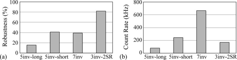
Simulation results for the four comparator and clock generator design combinations listed in Table 1: (a) robustness, and (b) maximum count rate obtained for each design. See text for further details.
For each simulation that passed all four timing requirements, a count rate was derived by taking the inverse of the shortest count period in the output of that simulation — defined as the time interval from the beginning of one φ1 to the beginning of the next φ1, as illustrated in Fig. 10. A maximum output count rate was established for each design based on the fastest variation of that design — resulting in rates of ~80, 250, 650, and 175 kHz for the 5inv-long, 5inv-short, 7inv, and 3inv-2SR designs, respectively, as illustrated in Fig. 11b.
As seen in Fig. 11, the first three designs (i.e., 5inv-long, 5inv-short, and 7inv) have much lower robustness compared to the 3inv-2SR design, and exhibit a wide range of maximum output count rates. This lower robustness can be largely attributed to the single SR-latch circuit architecture common to all three designs that, under certain combinations of tmin and model cards, can produce overlapping φ1 and φ2 pulses that result in violation of one or more of the four timing requirements. The wide range of maximum count rates can be attributed to the specific W-to-L ratios employed for the transistors in each of the three designs. For the 3inv-2SR design, the maximum count rate could be considerably increased (conceivably by an order of magnitude, or more) by modifying the W-to-L ratios in that design — without significantly affecting the favorably high robustness demonstrated in Fig. 11a since this design employs a circuit architecture (i.e., the dual SR-latch) which circumvents the possibility of generating overlapping pulses.
IIId. Results — Counter performance simulations
In the study, a counter variation was considered to be successful if it cycled through all 511 unique states before “looping” back to the starting state and repeating. For each counter design at each count rate, the number of successful variations divided by the total number of variations simulated (i.e., 200) is defined as the robustness.
Table 4 shows robustness as a function of count rate for the three counter designs. The Differential-Res and Differential-TFT designs are seen to demonstrate good robustness (i.e., above 90%) up to 1 MHz. Above 1 MHz, robustness for these designs falls off sharply — a result of how the bits of the designs change their stored values. For both designs, a value is stored within the bit by means of a self-reinforcing feedback loop and, in order to change the value of a bit, a certain amount of time is needed in order to overcome this feedback loop and store a new value. The amount of time required to store a new value depends on the quality of the TFTs in the circuit, which is affected by TFT variations. For example, a counter bit comprised of low-mobility TFTs will require a longer time in order to store a new value — resulting in increasing likelihood for that counter to fail at higher count rates.
Table 4.
Robustness results from simulation of the three counter designs shown in Fig. 5 as a function of count rate.
| Count rate (MHz) | 0.1 | 0.25 | 0.5 | 1 | 2 | 3 |
|---|---|---|---|---|---|---|
| Differential-Res | 97% | 97% | 96.5% | 92.5% | 4% | 0% |
| Differential-TFT | 100% | 100% | 100% | 99.5% | 72.5% | 33% |
| Gated-bit | 100% | 100% | 100% | 100% | 100% | 94% |
The gated-bit design, on the other hand, demonstrates good robustness across the entire range of simulated count rates. This design also employs a self-reinforcing feedback loop in order to store a value, but a gating transistor is used to disconnect the feedback loop when storing a new value — greatly decreasing the time needed to store a new value and thus making the design more tolerant of TFT variations at higher count rates.
IIIe. Results — Minimum pixel pitch calculations
In Fig. 12, the minimum pixel pitch and total circuit area of the components and common wires for the circuit designs of the Pxl3 and Pxl5 prototypes are shown as a function of conceivable, progressive improvement in the layout and fabrication of poly-Si PCAs. In the figure, the improvement labeled Im1 corresponds to the original design specifications of the prototypes (i.e., a minimum feature size of 6 μm and 4 metal layers), but with unoccupied pixel area excluded. Under these conditions, the circuit designs of Pxl3 and Pxl5 would have pixel pitches of ~835 and 672 μm, respectively. Im2 corresponds to a reduction in minimum feature size to 3 μm — resulting in pixel pitches of ~693 and 598 μm for Pxl3 and Pxl5. Im3 corresponds to a further reduction in minimum feature size to 1 μm — resulting in pixel pitches of ~578 and 544 μm for Pxl3 and Pxl5. From these results, it is apparent that decreasing minimum feature size provides diminishing benefit, and the area occupied by common wires becomes the dominant factor in determining minimum pixel pitch. Accordingly, increasing the number of metal layers by 4 (corresponding to Im4) reduces pixel pitch to ~290 and 243 μm for Pxl3 and Pxl5.
Figure 12.

Bar graph illustrating the total circuit area for the circuit designs of the (a) Pxl3 and (b) Pxl5 prototypes as a function of progressive improvement in the layout and fabrication of these designs — as detailed in the main text. For each bar, the areas occupied by the amplifier, comparator, clock generator, and counter components, as well as the common wires, are indicated by different shadings. The number appearing above each bar is the pixel pitch corresponding to the total circuit area.
IV. Discussion
In this study, simulation modeling has been used to examine the potential performance of prototype PCAs based on large-area poly-Si TFT process technology. The frameworks employed in the study enable examination of the influence of individual transistors within photon counting circuits on circuit performance (a level of detail that is not normally accessible through empirical measurement) and provide insight into how the circuits can be improved. From the results of this study, a number of interesting observations can be made.
The analog simulation framework employed frequency-domain simulations (to determine signal and noise) in order to calculate SNR values for the amplifier designs. A more precise, but also more computationally intensive, determination of SNR could be achieved by means of time-domain simulations for signal and noise, while also utilizing a more advanced poly-Si transistor noise model that scales the noise depending on the operating condition of each transistor (whereas the current study utilized averaged kf values derived from a range of operating conditions).
For the digital simulation framework, the methodology adopted for this study helps to identify those designs that best cope with non-uniformities in poly-Si TFT signal characteristics from substrate to substrate — as well as help to minimize the number of pixels on a given substrate which do not meet specified criteria. While the present study was limited to an examination of component circuits corresponding to recently fabricated prototypes, the methodology can be used to guide development of new circuit designs that meet even more demanding criteria (e.g., higher output count rates for the comparator+clock generator) while maintaining a high degree of robustness.
In order for a PCA to be clinically practical for diagnostic imaging, the pixels would be required to handle input x-ray count rates (in units of mega-counts per second per mm2) on the order of 1 to 50 Mcps/mm2 (Abbene et al., 2010; Taguchi et al., 2011). By comparison, PCAs based on c-Si have reported maximum count rate capabilities ranging from 1 to 600 Mcps/mm2 (Taguchi and Iwanczyk, 2013). Given that the minimum pixel pitch predicted in this study is on the order of 250 μm, the expected input x-ray count rates for such a pixel size would be ~0.06 to 3.1 Mcps (i.e., one-sixteenth of the estimated rates per mm2 cited above). In an array, since the maximum count rate capability per pixel is generally limited by that of the slowest component, it was of interest in the current study to examine the maximum count rates (expressed in units of MHz) of individual components of the SPC1 PCA circuit. The count rates for the designs exhibiting the highest robustness were ~0.175 and 3 MHz for the comparator+clock generator (3inv-2SR) and counter (gated-bit) components, respectively. (The count rates of the amplifier designs were not evaluated in this study.) While these count rates compare favorably with the expected input x-ray count rates, the comparator+clock generator components would limit the maximum count rate for the overall pixel. However, given that the circuits evaluated in this paper only represent initial poly-Si designs, it is strongly anticipated that higher rates can be achieved while maintaining high robustness.
Given the large number of circuit elements in a PCA design, pixel pitch can be minimized, to a degree, through judicious choice of circuit designs without detrimental effect on performance. For example, the Pxl5 design not only allows a smaller pixel pitch compared to Pxl3, its comparator+clock generator and counter components were identified as those with the highest robustness (and, in the case of the counter, the highest count rate as well). Further reduction in pixel pitch can be obtained through improvement in the poly-Si fabrication technology. The minimum pixel pitch estimates reported in this study were based on published and/or conceivable improvements in that technology. Of the 3 process-related improvements investigated, both an increase in the number of metal layers from 4 to 8 and a reduction in minimum feature size from 6 to 3 μm are readily achievable with current fabrication techniques — while employing a 1 μm minimum feature size is not commercially available at this time, but may be in the future. Reduction in pixel pitch can also be achieved by redesigning circuits (to better optimize their layouts or to decrease the number of transistors) or by reducing the number of common wires needed to operate the array (for example, through introduction of multiplexing).
The results of this initial study of the theoretical performance of the pixel circuit components used in the first prototype PCAs based on poly-Si TFTs are encouraging. We anticipate that such information, along with results obtained from planned empirical characterizations of the SPC1 PCAs, will form a starting point for future optimization of poly-Si based PCAs exhibiting higher robustness, increased count rate, and smaller pitch.
Acknowledgments
The authors would like to thank John McDonald, Mike Yeakey, Alan Young, and Chuck Martelli from the Michigan group for technical support in the design, assembly, and maintenance of the computational cluster used to perform the simulations in this study. This research was partially funded by NIH grant R01 EB000558.
Contributor Information
Albert K. Liang, Department of Radiation Oncology, University of Michigan, Ann Arbor, MI 48109
Martin Koniczek, Department of Radiation Oncology, University of Michigan, Ann Arbor, MI 48109.
Larry E. Antonuk, Department of Radiation Oncology, University of Michigan, Ann Arbor, MI 48109.
Youcef El-Mohri, Department of Radiation Oncology, University of Michigan, Ann Arbor, MI 48109.
Qihua Zhao, Department of Radiation Oncology, University of Michigan, Ann Arbor, MI 48109.
Robert A. Street, Palo Alto Research Center (PARC), Palo Alto, CA 94304
Jeng Ping Lu, Palo Alto Research Center (PARC), Palo Alto, CA 94304.
References
- Abbene L, Gerardi G, Principato F, Del Sordo S, Ienzi R, Raso G. High-rate x-ray spectroscopy in mammography with a CdTe detector: A digital pulse processing approach. Med Phys. 2010;37:6147–56. doi: 10.1118/1.3512804. [DOI] [PubMed] [Google Scholar]
- Ballabriga R, Campbell M, Heijne E, Llopart X, Tlustos L, Wong W. Medipix3: A 64 k pixel detector readout chip working in single photon counting mode with improved spectrometric performance. Nucl Instr and Meth. 2011;A 633:S15–S8. [Google Scholar]
- Barber WC, Nygard E, Iwanczyk JS, Zhang M, Frey EC, Tsui BM, Wessel JC, Malakhov N, Wawrzyniak G, Hartsough NE, Gandhi T, Taguchi K. Characterization of a novel photon counting detector for clinical CT: count rate, energy resolution, and noise performance. Proc SPIE. 2009;7258:725824. [Google Scholar]
- Boyce JB, Fulks RT, Ho J, Lau R, Lu JP, Mei P, Street RA, Van Schuylenbergh KF, Wang Y. Laser processing of amorphous silicon for large-area polysilicon imagers. Thin Solid Films. 2001;383:137–42. [Google Scholar]
- Campbell M, Heijne E, Meddeler G, Pernigotti E, Snoeys W. A readout chip for a 64×64 pixel matrix with 15-bit single photon counting. IEEE Transactions on Nuclear Science. 1998;45:751–3. [Google Scholar]
- El-Mohri Y, Antonuk LE, Koniczek M, Zhao Q, Li Y, Street RA, Lu JP. Active pixel imagers incorporating pixel-level amplifiers based on polycrystalline-silicon thin-film transistors. Med Phys. 2009;36:3340–55. doi: 10.1118/1.3116364. [DOI] [PMC free article] [PubMed] [Google Scholar]
- Fischer P, Helmich A, Lindner M, Wermes N, Blanquart L. A photon counting pixel chip with energy windowing. IEEE Transactions on Nuclear Science. 2000;47:881–4. [Google Scholar]
- Fredenberg E, Lundqvist M, Aslund M, Hemmendorff M, Cederstrom B, Danielsson M. A photon-counting detector for dual-energy breast tomosynthesis. Proc SPIE. 2009;7258:72581J. [Google Scholar]
- Fredenberg E, Lundqvist M, Cederstrom B, Aslund M, Danielsson M. Energy resolution of a photon-counting silicon strip detector. Nucl Instr and Meth. 2010;A613:156–62. [Google Scholar]
- Iniguez B, Xu Z, Fjeldly TA, Shur MS. Unified model for short-channel poly-Si TFTs. Solid-State Electronics. 1999;43:1821–31. [Google Scholar]
- Li Y, Antonuk LE, El-Mohri Y, Zhao Q, Du H, Sawant A, Wang Y. Effects of x-ray irradiation on polycrystalline silicon, thin-film transistors. J Appl Phys. 2006;99:064501–1. to -7. [Google Scholar]
- Liang AK, Koniczek M, Antonuk LE, El-Mohri Y, Zhao Q, Jiang H, Street RA, Lu JP. Initial steps toward the realization of large area arrays of single photon counting pixels based on polycrystalline silicon TFTs. Proc SPIE. 2014;9033:90331I. [Google Scholar]
- Limousin O. New trends in CdTe and CdZnTe detectors for X- and gamma-ray applications. Nucl Instr and Meth. 2003;A 504:24–37. [Google Scholar]
- Llopart X, Campbell M, Dinapoli R, San Segundo D, Pernigotti E. Medipix2: A 64-k pixel readout chip with 55-um square elements working in single photon counting mode. IEEE Transactions on Nuclear Science. 2002;49:2279–83. [Google Scholar]
- Locker M, Fischer P, Krimmel S, Kruger H, Lindner M, Nakazawa K, Takahashi T, Wermes N. Single photon counting X-ray imaging with Si and CdTe single chip pixel detectors and multichip pixel modules. IEEE Transactions on Nuclear Science. 2004;51:1717–23. [Google Scholar]
- Lundqvist M, Danielsson M, Cederstrom B, Chmill V, Chuntonov A, Aslund M. Measurements on a full-field digital mammography system with a photon counting crystalline silicon detector. Proc SPIE. 2003;5030:547–52. [Google Scholar]
- Perenzoni M, Stoppa D, Malfatti M, Simoni A. A multispectral analog photon-counting readout circuit for X-ray hybrid pixel detectors. IEEE Trans Instrum Meas. 2008;57:1438–44. [Google Scholar]
- Razavi B. Design of analog CMOS integrated circuits. Tata McGraw-Hill Education; 2002. [Google Scholar]
- Schlomka J, Roessl E, Dorscheid R, Dill S, Martens G, Istel T, Baumer C, Herrmann C, Steadman R, Zeitler G, Livne A, Proksa R. Experimental feasibility of multi-energy photon-counting K-edge imaging in pre-clinical computed tomography. Physics in Medicine and Biology. 2008;53:4031–47. doi: 10.1088/0031-9155/53/15/002. [DOI] [PubMed] [Google Scholar]
- Shikhaliev PM, Fritz SG. Photon counting spectral CT versus conventional CT: comparative evaluation for breast imaging application. Physics in Medicine and Biology. 2011;56:1905–30. doi: 10.1088/0031-9155/56/7/001. [DOI] [PubMed] [Google Scholar]
- Taguchi K, Iwanczyk JS. Vision 20/20: Single photon counting x-ray detectors in medical imaging. Med Phys. 2013;40:100901. doi: 10.1118/1.4820371. [DOI] [PMC free article] [PubMed] [Google Scholar]
- Taguchi K, Zhang M, Frey EC, Wang X, Iwanczyk JS, Nygard E, Hartsough NE, Tsui BM, Barber WC. Modeling the performance of a photon counting x-ray detector for CT: Energy response and pulse pileup effects. Med Phys. 2011;38:1089–102. doi: 10.1118/1.3539602. [DOI] [PMC free article] [PubMed] [Google Scholar]
- Tokuda S, Adachi S, Sato T, Yoshimuta T, Nagata H, Uehara K, Izumi Y, Teranuma O, Yamada S. Experimental evaluation of a novel CdZnTe flat-panel x-ray detector for digital radiography and fluoroscopy. Proc SPIE. 2001;4320:140–7. [Google Scholar]
- Tsividis Y, McAndrew C. Operation and Modeling of the MOS Transistor. Oxford Univ. Press; 2011. [Google Scholar]