

Abstract
Two-dimensional (2D) crystals offer a unique platform due to their remarkable and contrasting spintronic properties, such as weak spin–orbit coupling (SOC) in graphene and strong SOC in molybdenum disulfide (MoS2). Here we combine graphene and MoS2 in a van der Waals heterostructure (vdWh) to demonstrate the electric gate control of the spin current and spin lifetime at room temperature. By performing non-local spin valve and Hanle measurements, we unambiguously prove the gate tunability of the spin current and spin lifetime in graphene/MoS2 vdWhs at 300 K. This unprecedented control over the spin parameters by orders of magnitude stems from the gate tuning of the Schottky barrier at the MoS2/graphene interface and MoS2 channel conductivity leading to spin dephasing in high-SOC material. Our findings demonstrate an all-electrical spintronic device at room temperature with the creation, transport and control of the spin in 2D materials heterostructures, which can be key building blocks in future device architectures.
Two-dimensional materials are unique to build heterostructures with contrasting spintronic properties. Here, Dankert and Dash utilize a van der Waals heterostructure with graphene and MoS2 to demonstrate an all-electrical device for creation, transport and control of the spin current up to room temperature.
Spintronics aims to exploit the spin degree of freedom in solid state devices for data storage and information processing technologies1,2. The fundamental spintronic device concepts, such as creation, manipulation and detection of spin current has been demonstrated in semiconductors3,4,5 and spin transistor structures6,7,8,9 using both electrical and optical methods. However, an unsolved challenge in the field is the realization of all-electrical methods to control the spin current and spin lifetime at ambient temperature2. For this purpose, two-dimensional (2D) crystals offer a unique platform for spintronics due to their remarkably broad range of spin-dependent properties10,11,12. Graphene has been demonstrated as an excellent material for spin transport and spin logic devices due to the low spin–orbit coupling (SOC) and high electron mobility11,12,13,14,15,16,17,18,19,20. However, this low SOC causes a big challenge for the electrical control of the spin polarization in graphene11,12. In contrast, transition metal di-chalcogenides (TMDCs) are semiconductors with a high SOC, several 10 meV in the conduction band and 100 meV in the valence band, which are orders of magnitude higher than in graphene11,21. Recently, such high-SOC TMDCs also showed fascinating spin dynamics and transport properties22,23,24,25.
To harvest these novel and contrasting spintronic properties of both 2D materials, hybrid devices, consisting of graphene and TMDC van der Waals heterostructures (vdWh)26,27, are proposed to be promising28. The proximity-induced strong SOC of graphene/TMDC vdWhs led to the observation of weak anti-localization29,30 and spin Hall effect31. In addition to the advantage of spin transport in graphene, SOC in such vdWhs can be utilized to electrically control the spin polarization. Recently, a spin field-effect switch has been demonstrated by using non-local (NL) spin-valve measurements in such a vdWh up to 200 K (ref. 32). For comprehensive understanding and advancement of 2D materials vdWh-based spintronic devices, demonstration of electrical gate-tunable spin current and spin lifetime by both spin-valve and Hanle spin precession measurements at ambient temperatures is a crucial requirement.
In this article, we demonstrate the electronic gate control of the spin current and spin lifetime at room temperature by using both spin-valve and Hanle measurements on graphene/MoS2 vdWh devices. Hanle spin precession measurements unambiguously prove the spin-polarized transport and demonstrate the electrical gate control of the spin lifetime and diffusion length in such 2D material heterostructures at room temperature. We further prove that the gate-voltage tuning of the Schottky barrier at the graphene–MoS2 interface and MoS2 channel conduction facilitate the spin in graphene to interact and dephase efficiently in high-SOC material MoS2. Extensive spintronic and electronic measurements in different devices at various gate voltages, injection bias currents and temperatures enable us to understand the gate control of spin relaxation mechanism in such vdWhs.
Results
Device and electrical gate control of spin current
A schematic representation of a gate-controlled graphene/MoS2 vdWh spintronic device used for both spin-valve and Hanle measurements is shown in Fig. 1a. We fabricated the heterostructure devices with large-area chemical vapour deposited (CVD) graphene13 and TMDC molybdenum disulfide (MoS2) flakes22 (Fig. 1b). The spin current is generated and detected in NL measurement geometry by using ferromagnetic (FM) tunnel contacts deposited on graphene either in parallel or antiparallel magnetization configuration (see ‘Methods’ section)13. Our devices satisfy the four main requirements for a transistor-like spin signal modulation at room temperature:33 the electrical creation, diffusive transport, NL electrical detection and the crucial electrical control of a spin current by means of a gate voltage. Figure 1c shows the gate dependence of the measured spin signal modulation, demonstrating transistor-like ON/OFF states at room temperature. The measurements were performed by probing the NL voltage (ΔVNL) while sweeping the gate voltage (Vg), for both parallel and antiparallel magnetization alignments of FM source and drain. To confirm such a gate-controlled spin device operations and to understand the spin relaxation mechanisms, we systematically investigated both the spin valve and Hanle spin precession measurements in graphene/MoS2 heterostructures.
Figure 1. MoS2/graphene vdWh.

(a) Schematics of graphene/MoS2 heterostructure channel with FM source (S) and drain (D) contacts. This structure allows spin injection into graphene from the source (S), diffusive spin transport in the graphene/MoS2 channel, spin manipulation by a gate voltage and detection of spin signal by the drain (D). (b) Coloured scanning electron microscope image of a fabricated device with a CVD graphene/MoS2 heterostructure channel and multiple FM tunnel contacts of TiO2(1 nm)/Co(80 nm) (scale bar, 1 μm). The devices are fabricated on Si/SiO2 substrate, which is used as a gate electrode for control of the spin polarization in the channel. (c) Gate dependence of the measured NL resistance  normalized to the maximum value, showing transistor-like ON/OFF spin signal modulation at room temperature, for parallel and antiparallel magnetization alignments of source and drain.
Electrical gate control of spin-valve signal
To investigate the spin transport behaviour in the graphene/MoS2 heterostructure channel, spin-valve measurements were performed in NL geometry at room temperature. Sweeping an in-plane magnetic field, the magnetization configuration of the injector and detector FM contacts (Fig. 2a) can be aligned parallel or antiparallel, resulting in a magnetoresistance ΔRNL. We observed a clear spin-valve signal (Fig. 2b) at room temperature, demonstrating the possibility of spin transport in the graphene/MoS2 heterostructures with a channel length of 2.6 μm and a width of 0.6 μm. The NL spin-valve signal  is smaller than usually measured in pristine CVD graphene channels of similar geometry13. This reduction could arise from SOC induced in the graphene channel in proximity with MoS2 (refs 28, 29, 30, 31).
Figure 2. Gate-controlled spin valve signal at room temperature.

(a) Schematic of the NL spin-valve measurement geometry, where the spin current injector circuit (I) and the voltage detector circuit (V) are placed in a NL geometry. The spin current diffusing in the heterostructure channel is detected as a voltage signal by the FM detector. The magnetization of the injector/detector FM contact and also the sign of spin accumulation are controlled by an in-plane magnetic field B||. (b) NL spin-valve magnetoresistance  measurements at 300 K by application of different gate voltages Vg. Measurements are performed at a constant current source of I=30 μA. A NL linear background (few μV) due to stray charge current is subtracted from the signal. (c) Modulation of spin-valve signal magnitude ΔRNL with gate voltage Vg, showing ON/OFF states at 300 K. The error bar is derived from the root mean square of the noise in the measured signal.
Next, we measured the spin-valve signal at different gate voltages (Vg) at room temperature (Fig. 2b,c). Below a threshold voltage Vg<0 V, we observed spin-valve signals ΔRNL with almost constant amplitude. For the gate-voltage range of 0<Vg<50 V, a drastic reduction in ΔRNL is observed, whereas for Vg>50 V no spin signal could be detected. This behaviour reproduces the gate sweep NL resistance modulation behaviour we also measured in Fig. 1c. The strong modulation and vanishing spin current from ON to OFF state with application of gate voltage in our MoS2/graphene heterostructures indicates an electrical spin-control operation at room temperature. Spin-valve measurements with similar behaviour are recently reported at lower temperatures up to 200 K (ref. 32). The room temperature gate control in our spintronic devices can be attributed to better spin transport properties in graphene samples and less interfacial scattering. To further confirm the spin transport and to estimate the spin relaxation time, gate-dependent Hanle spin precession measurements in the graphene/MoS2 channel are necessary.
Electrical gate control of spin lifetime
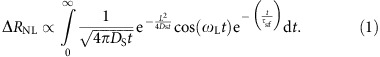
Consequently, we performed NL Hanle spin precession measurements in our graphene/MoS2 vdWh devices (Fig. 3a). Figure 3b shows the Hanle data measured for different gate voltages at room temperature. In this geometry, the modulation of the signal stems from the spin precession about a perpendicular magnetic field  with the Larmor frequency
  (Landé factor g=2)34,35. The variation of this NL resistance ΔRNL due to precession and relaxation of the spins diffusing from the injector to the detector can be described by:
Figure 3. Gate-controlled Hanle spin precession at room temperature.

(a) NL Hanle geometry, where source and drain magnetization are aligned parallel while sweeping a perpendicular magnetic field  . (b) NL Hanle spin signal
  measured at 300 K at different gate voltages. Measurements are performed at a constant current source of I=30 μA. The raw data points are fitted with equation (1) (red line) to extract spin lifetime τsf and diffusion length λsf. (c) The gate voltage Vg dependence of spin lifetime τsf (black) and diffusion length λsf (orange) at 300 K showing modulation of spin parameters from ON to OFF state. The error is derived from the error of the Hanle fit.
 |
With the channel length L, we can extract the spin lifetime τsf and diffusion constant  to calculate the spin diffusion length
  (Fig. 3c). Similar to the spin-valve measurements, we observed an almost constant Hanle signal for Vg<0 V (Fig. 3b). In this range, we obtain a spin lifetime
 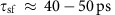 and diffusion length
  at room temperature. The reduced spin lifetime in our vdWhs, compared to pristine graphene devices (200–300 ps)13, indicates a proximity-induced SOC in graphene through MoS2. Such a shortened spin lifetime has also been expected using the spin–orbit relaxation time τso determined from spin Hall effect studies31, weak anti-localization measurements29,30 and theoretical predictions28,32. The
  in our graphene in proximity with MoS2 corresponds to ∼1 meV of spin splitting at room temperature, which is gigantic compared to the few μeV in pristine graphene28. The induced SOC in graphene in proximity with MoS2 can be attributed to the hybridization of the carbon orbitals with the d orbitals of Mo (ref. 28). In the gate-voltage range of 0 V<Vg<25 V, a strong tuning of the spin signal amplitude ΔRNL, spin lifetime τsf and consequently diffusion length λsf in the MoS2/graphene channel is observed. The τsf can be tuned down to ∼5 ps near Vg=25 V. For Vg>25 V, the Hanle signal could not be observed, validating a transition from ON to OFF state with gate voltage. This realization of a gate-controlled spin lifetime by an order of magnitude opens fascinating prospect for spin transport and spin relaxation in such graphene/TMDC hybrid systems.
The disappearance of the Hanle signal already at a gate voltage of about 30 V is due to the reduction of the amplitude by factor two compared to the spin-valve signal, which is consistent with the measurement principle (see Supplementary Fig. 1). Comparative measurements in a pristine graphene channel revealed only a weak modulation in ΔRNL and τsf due to a change in carrier density around the Dirac point13. The observed strong modulation and vanishing spin signal in our vdWhs can originate from the gate-controlled interaction of spin-polarized electrons in graphene with high-SOC MoS2. This electrical control of spin signal is reproducibly observed over several devices fabricated on different chips and measured at various bias voltages, gate-voltage sweeps and temperatures (see Supplementary Figs 2–4).
Discussion
To understand the gate-controlled spin modulation, we characterized the charge transport in both the MoS2 channel and the graphene/MoS2 vdWhs. The lateral MoS2 field-effect transistor shows a typical n-type transfer characteristic with an enhancement of current up to 106 times with application of Vg at room temperature (see Supplementary Fig. 5). Such a gate-tunable MoS2 channel resistance in our MoS2/graphene vdWh would allow the tuning of a parallel spin transport channel next to graphene. If the spin current from graphene can enter MoS2 in the ON state, spins would lose their coherence at a much faster rate, due to the high SOC of MoS2.
Next, we investigated the charge transport in vertical graphene/MoS2 devices, to understand the transport mechanisms at the interface (Fig. 4a). The transfer characteristic of such a device is typical for n-type field effect transistors with a current enhancement of more than 102 times (ON/OFF) at room temperature (Fig. 4b). The corresponding output characteristic shows an asymmetric line shape in the OFF state, which becomes symmetric in the ON state (Fig. 4c). This transistor behaviour can be attributed to the presence of a gate-tunable Schottky barrier (Ф) at the MoS2/graphene interface36,37. We determined this barrier Ф from the temperature-dependent output characteristic using the thermionic emission model22,36 (see Supplementary Fig. 6). Figure 4d shows the gate dependence of Ф at the graphene/MoS2 interface, which changes from 300 to 50 meV when tuning the vertical transistor from OFF to ON state. This corresponds to a gate modulation of the graphene Fermi level with respect to the MoS2 conduction band as depicted in the insets of Fig. 4d. Consequentially, in the spin-ON state, a high Schottky barrier at the graphene/MoS2 interface and high-channel resistance of MoS2 prevents spins in the graphene to enter the MoS2 channel (Fig. 4e). In contrast, in the spin-OFF state, the Schottky barrier at the graphene/MoS2 interface is significantly reduced yielding an almost Ohmic contact, in addition to a drastic reduction in MoS2 channel resistance (Fig. 4f). Under these conditions, spins can easily enter MoS2, where they experience a much faster spin relaxation. This explains the reduction in spin lifetime in addition to the decrease in spin signal amplitude with gate voltage in our spin-modulation device. These findings demonstrate that the gate voltage can tune the band offset between materials having complementary spintronics properties, facilitating the spins in graphene to interact efficiently with MoS2.
Figure 4. Tuning the Schottky barrier at the MoS2/graphene interface by gate voltage.

(a) Schematics of the graphene/MoS2 vertical heterostructure. (b) Transfer characteristic (drain–source current Ids versus gate voltage Vg for different drain–source voltages Vds) in a vertical device with MoS2 thickness of 35 nm. (c) Output characteristics (Ids versus Vds) at  . (d) Schottky barrier height Ф obtained for different Vg. Inset: Band structures at the MoS2/graphene interface for Vg<0 V and Vg>30 V. (e) Representative circuit diagram of the graphene and MoS2 parallel transport channels connected by Schottky barrier resistors in the heterostructure. At gate voltages Vg<0 V, the large Schottky barrier and high MoS2 resistance prevents spins from interacting with the high SOC MoS2 channel, resulting in a finite spin transport in graphene and corresponds to the spin-ON state. (f) At high gate voltages Vg>30 V, the reduced Schottky barrier and MoS2 channel resistance allows spins to tunnel into MoS2 and hence dephasing in the high-SOC material, resulting in the spin-OFF state.
In conclusion, the realization of the electrical control of spin current at room temperature using 2D material heterostructures is a significant step in the field of spintronics. Exploiting the complementary spintronic properties of graphene and MoS2 creates a unique platform, where the spin current can be tuned in a controlled manner by gate voltage. Combining the gate dependence studies of spin valve, Hanle spin precession and Schottky barrier control in graphene/MoS2 heterostructures, we experimentally demonstrate the remarkable control over the spin parameters. The all-electrical creation, transport and control of the spins in vdWhs also demonstrated an integration of novel gate-controlled spin device and non-volatile FM memory elements. The spin-ON state current can be increased by integrating FM source and drain contacts of Heusler alloys with high spin polarization20. The graphene/MoS2 spintronic devices can be further improved by introducing insulating hexagonal boron nitride (h-BN) as tunnel barrier for efficient spin injection38,39, for gate-controlled spin polarization via magnetic proximity effects40, h-BN as substrate for improved graphene properties41,42, and as ultra-thin gate dielectric for efficient gate control of the spin parameters in the channel. Our findings also open a new platform for the interplay of spin, charge and orbital degrees of freedom for testing a plethora of exotic physical phenomena. Consequently, novel electronic materials with tunable SOC in electron- and hole-doped regime43 and emerging materials with topological protection44 can be used in heterostructures with graphene to create novel spin phenomena and provide opportunities for new discoveries.
Methods
Device fabrication
The vdWhs were prepared using CVD graphene (Graphenea) on highly doped Si (with a thermally grown 285-nm-thick SiO2 layer) and cleaned by Ar/H2 annealing at 450 °C. The MoS2 flakes (single crystals from SPI supplies) were transferred on top of graphene, which was patterned into individual channels either before or after the MoS2 transfer. The graphene was patterned by photo- or electron beam lithography and oxygen plasma etching. Next, appropriate MoS2 flakes of ∼20–35 nm located on graphene were identified by an optical microscope for device fabrication. The contacts were patterned on graphene (and MoS2 flakes, in case of the vertical devices) by electron beam lithography. Finally, we used electron beam evaporation to deposit 8 Å Ti, followed by in situ oxidation in a pure oxygen atmosphere for 30 min, resulting in an about 1 nm thick TiO2 layer. Without interrupting the vacuum, we deposited 80 nm Co and finalized the devices by lift-off in warm acetone at 60 °C. In the final devices, the Co/TiO2 contacts on graphene act as source and drain for spin-polarized electrons, the MoS2/graphene heterostructure region used as the channel and the Si/SiO2 is used as a gate for manipulation of the spin polarization. A representative Dirac curve for the graphene vdWhs is shown in Supplementary Fig. 7.
Measurements
The measurements were performed in a cryostat with variable temperature and magnetic field facility. The current is applied using a Keithley 6221 current source and the NL voltage is detected by a Keithley 2182A nanovoltmeter; the gate voltage was applied using a Keithley 2612 source metre.
Data availability
The data that support the findings of this study are available from the corresponding authors on reasonable request.
Additional information
How to cite this article: Dankert, A. & Dash, S. P. Electrical gate control of spin current in van der Waals heterostructures at room temperature. Nat. Commun. 8, 16093 doi: 10.1038/ncomms16093 (2017).
Publisher’s note: Springer Nature remains neutral with regard to jurisdictional claims in published maps and institutional affiliations.
Supplementary Material
Acknowledgments
The authors acknowledge financial supports from EU Graphene Flagship (No. 604391), EU FlagEra project (from Swedish Research council VR No. 2015-06813), Swedish Research Council VR project grants (No. 2016-03658), Graphene center and the AoA Nano program at Chalmers University of Technology. The authors also acknowledge the support of colleagues at the Quantum Device Physics Laboratory and Nanofabrication Laboratory at Chalmers University of Technology.
Footnotes
The authors declare no competing financial interests.
Author contributions A.D. and S.P.D conceived the idea and designed the experiments. A.D. carried out the device fabrication and measurements. S.P.D. supervised the research. A.D. and S.P.D. analysed the data and wrote the manuscript.
References
- Žutić I., Fabian J. & Sarma S. Das. spintronics: fundamentals and applications. Rev. Mod. Phys. 76, 323–410 (2004). [Google Scholar]
- Awschalom D. D. & Flatté M. E. Challenges for semiconductor spintronics. Nat. Phys. 3, 153–159 (2007). [Google Scholar]
- Dash S. P., Sharma S., Patel R. S., de Jong M. P. & Jansen R. Electrical creation of spin polarization in silicon at room temperature. Nature 462, 491–494 (2009). [DOI] [PubMed] [Google Scholar]
- Ohno Y. et al. Electrical spin injection in a ferromagnetic semiconductor heterostructure. Nature 402, 790–792 (1999). [Google Scholar]
- Jansen R., Min B.-C. & Dash S. P. Oscillatory spin-polarized tunnelling from silicon quantum wells controlled by electric field. Nat. Mater. 9, 133–138 (2010). [DOI] [PubMed] [Google Scholar]
- Datta S. & Das B. Electronic analog of the electro-optic modulator. Appl. Phys. Lett. 56, 665–667 (1990). [Google Scholar]
- Chuang P. et al. All-electric all-semiconductor spin field-effect transistors. Nat. Nanotechnol. 10, 35–39 (2014). [DOI] [PubMed] [Google Scholar]
- Koo H. C. et al. Control of spin precession in a spin-injected field effect transistor. Science 325, 1515–1518 (2009). [DOI] [PubMed] [Google Scholar]
- Wunderlich J. et al. Spin Hall effect transistor. Science 330, 1801–1804 (2010). [DOI] [PubMed] [Google Scholar]
- Tombros N., Jozsa C., Popinciuc M., Jonkman H. T. & van Wees B. J. Electronic spin transport and spin precession in single graphene layers at room temperature. Nature 448, 571–574 (2007). [DOI] [PubMed] [Google Scholar]
- Han W., Kawakami R. K., Gmitra M. & Fabian J. Graphene spintronics. Nat. Nanotechnol. 9, 794–807 (2014). [DOI] [PubMed] [Google Scholar]
- Roche S. et al. Graphene spintronics: the European Flagship perspective. 2D Mater. 2, 30202 (2015). [Google Scholar]
- Kamalakar V. M., Groenveld C., Dankert A. & Dash S. P. Long distance spin communication in chemical vapour deposited graphene. Nat. Commun. 6, 6766 (2015). [DOI] [PMC free article] [PubMed] [Google Scholar]
- Avsar A. et al. Electronic spin transport in dual-gated bilayer graphene. NPG Asia Mater. 8, e274 (2016). [Google Scholar]
- Shiraishi M. et al. Robustness of spin polarization in graphene-based spin valves. Adv. Funct. Mater. 19, 3711–3716 (2009). [Google Scholar]
- Friedman A. L., van ’t Erve O. M. J., Robinson J. T., Whitener K. E. & Jonker B. T. Hydrogenated graphene as a homoepitaxial tunnel barrier for spin and charge transport in graphene. ACS Nano 9, 6747–6755 (2015). [DOI] [PubMed] [Google Scholar]
- Dankert A., Kamalakar M. V., Bergsten J. & Dash S. P. Spin transport and precession in graphene measured by nonlocal and three-terminal methods. Appl. Phys. Lett. 104, 192403 (2014). [Google Scholar]
- Raes B. et al. Determination of the spin-lifetime anisotropy in graphene using oblique spin precession. Nat. Commun. 7, 11444 (2016). [DOI] [PMC free article] [PubMed] [Google Scholar]
- Wen H. et al. Experimental demonstration of xor operation in graphene magnetologic gates at room temperature. Phys. Rev. Appl. 5, 2331–7019 (2016). [Google Scholar]
- Yamaguchi T. et al. Spin injection into multilayer graphene from highly spin-polarized Co 2 FeSi Heusler alloy. Appl. Phys. Express 9, 63006 (2016). [Google Scholar]
- Mak K. F., Lee C., Hone J., Shan J. & Heinz T. F. Atomically thin MoS2: a new direct-gap semiconductor. Phys. Rev. Lett. 105, 136805 (2010). [DOI] [PubMed] [Google Scholar]
- Dankert A., Langouche L., Kamalakar M. V. & Dash S. P. High-performance molybdenum disulfide field-effect transistors with spin tunnel contacts. ACS Nano 8, 476–482 (2014). [DOI] [PubMed] [Google Scholar]
- Yang L. et al. Long-lived nanosecond spin relaxation and spin coherence of electrons in monolayer MoS2 and WS2. Nat. Phys. 11, 830–834 (2015). [Google Scholar]
- Song Y. & Dery H. Transport theory of monolayer transition-metal dichalcogenides through symmetry. Phys. Rev. Lett. 111, 026601 (2013). [DOI] [PubMed] [Google Scholar]
- Liang S. et al. Electrical spin injection and detection in molybdenum disulfide multilayer channel. Nat. Commun. 8, 14947 (2017). [DOI] [PMC free article] [PubMed] [Google Scholar]
- Geim A. K. & Grigorieva I. V. Van der Waals heterostructures. Nature 499, 419–425 (2013). [DOI] [PubMed] [Google Scholar]
- Novoselov K. S., Mishchenko A., Carvalho A., Neto A. H. C. & Road O. 2D materials and van der Waals heterostructures. Science 353, aac9439 (2016). [DOI] [PubMed] [Google Scholar]
- Gmitra M. & Fabian J. Graphene on transition-metal dichalcogenides: a platform for proximity spin-orbit physics and optospintronics. Phys. Rev. B Condens. Matter Mater. Phys. 92, 155403 (2015). [Google Scholar]
- Wang Z. et al. Strong interface-induced spin-orbit interaction in graphene on WS2. Nat. Commun. 6, 8339 (2015). [DOI] [PMC free article] [PubMed] [Google Scholar]
- Shi J. Tunable spin-orbit coupling and symmetry-protected edge states in graphene/WS2. 2D Mater. 3, 31011 (2016). [Google Scholar]
- Avsar A. et al. Spin–orbit proximity effect in graphene. Nat. Commun. 5, 4875 (2014). [DOI] [PubMed] [Google Scholar]
- Yan W. et al. A two-dimensional spin field-effect switch. Nat. Commun. 7, 13372 (2016). [DOI] [PMC free article] [PubMed] [Google Scholar]
- Sugahara S. & Nitta J. Spin-transistor electronics: an overview and outlook. in Proc. IEEE 98, 2124–2154 (2010). [Google Scholar]
- Johnson M. & Silsbee R. H. Interfacial charge-spin coupling: Injection and detection of spin magnetization in metals. Phys. Rev. Lett. 55, 1790–1793 (1985). [DOI] [PubMed] [Google Scholar]
- Johnson M. & Silsbee R. H. Coupling of electronic charge and spin at a ferromagnetic-paramagnetic metal interface. Phys. Rev. B 37, 5312–5325 (1988). [DOI] [PubMed] [Google Scholar]
- Yu W. J. et al. Vertically stacked multi-heterostructures of layered materials for logic transistors and complementary inverters. Nat. Mater. 12, 246–252 (2013). [DOI] [PMC free article] [PubMed] [Google Scholar]
- Moriya R. et al. Large current modulation in exfoliated-graphene/MoS2/metal vertical heterostructures. Appl. Phys. Lett. 105, 83119 (2014). [Google Scholar]
- Kamalakar M. V., Dankert A., Bergsten J., Ive T. & Dash S. P. Enhanced tunnel spin injection into graphene using chemical vapor deposited hexagonal boron nitride. Sci. Rep. 4, 6146 (2014). [DOI] [PMC free article] [PubMed] [Google Scholar]
- Kamalakar M. V., Dankert A., Kelly P. J. & Dash S. P. Inversion of spin signal and spin filtering in ferromagnet|hexagonal boron nitride-graphene van der Waals heterostructures. Sci. Rep. 6, 21168 (2016). [DOI] [PMC free article] [PubMed] [Google Scholar]
- Lazić P., Belashchenko K. D. & Žutić I. Effective gating and tunable magnetic proximity effects in two-dimensional heterostructures. Phys. Rev. B Condens. Matter Mater. Phys. 93, 241401 (2016). [Google Scholar]
- Ingla-Aynés J., Guimarães M. H. D., Meijerink R. J., Zomer P. J. & Van Wees B. J. 24-μ m spin relaxation length in boron nitride encapsulated bilayer graphene. Phys. Rev. B Condens. Matter Mater. Phys. 92, 201410 (2015). [Google Scholar]
- Drögeler M. et al. Spin lifetimes exceeding 12 ns in graphene nonlocal spin valve devices. Nano Lett. 16, 3533–3539 (2016). [DOI] [PubMed] [Google Scholar]
- Lee C.-H. et al. Atomically thin p–n junctions with van der Waals heterointerfaces. Nat. Nanotechnol. 9, 676–681 (2014). [DOI] [PubMed] [Google Scholar]
- Soumyanarayanan A., Reyren N., Fert A. & Panagopoulos C. Emergent phenomena induced by spin–orbit coupling at surfaces and interfaces. Nature 539, 509–517 (2016). [DOI] [PubMed] [Google Scholar]
Associated Data
This section collects any data citations, data availability statements, or supplementary materials included in this article.
Supplementary Materials
Data Availability Statement
The data that support the findings of this study are available from the corresponding authors on reasonable request.