Abstract
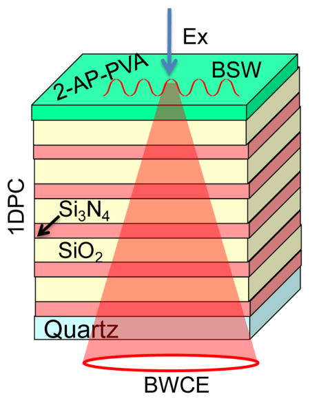
The interaction of fluorophores with nearby metallic structures is now an active area of research. Dielectric photonic structures offer some advantages over plasmonic structures, namely small energy losses and less quenching. We describe a dielectric one-dimensional photonic crystal (1DPC), which supports Bloch surface waves (BSWs) from 280 to 440 nm. This BSW structure is a quartz slide coated with alternating layers of SiO2 and Si3N4. We show that this structure displays BSWs and that the near-UV fluorophore, 2-aminopurine (2-AP), on the top surface of the structure couples with the BSWs. Fluorophores do not have to be inside the structure for coupling and show a narrow angular distribution, with an angular separation of wavelengths. The Bloch wave-coupled emission (BWCE) radiates through the dielectric layer. These BSW structures, with useful wavelength range for detection of intrinsic protein and cofactor fluorescence, provide opportunities for novel optical configurations for bioassays with surface-localized biomolecules and for optical imaging using the coupled emission.
Keywords: Bloch surface waves, One-dimensional photonic crystals, Bloch surface wave-coupled emission, Surface plasmon-coupled emission, 2-aminopurine, Plasmon-controlled fluorescence
Graphical Abstract
Bloch surface wave coupled emission from 2-aminopurine on one-dimensional photonic crystals with a useful wavelength range for detection of intrinsic protein and cofactor fluorescence.
Introduction
There is a growing interest in the use of nanostructures to modify or control fluorescence excitation and emission.1–3 Much of this research is motivated by the need for increased sensitivity and decreased complexity of instrumentation for fluorescence detection.4–6 Simplicity and decreased cost of the methodologies are especially needed for high-throughput applications like proteomics and DNA arrays.6 Nanostructures will play an important role in technology transfer from biotechnology to enable robust devices for self-testing and use in low research environments.7–9 One approach to achieve these goals has been the use of metallic particles and surfaces to increase fluorophore brightness and to use near-field fluorophore-metal interactions to obtain enhanced and/or directional emission.10–12 These efforts have been productive as can be seen from recent reviews on plasmon-controlled fluorescence.13–15 The nanoparticles of Ag and Au are used for probes with visible and near-IR spectral range. Aluminum, platinum and some other metal nanoparticles were reported to enhance signals from ultraviolet probes.16–23 We previously used Al nanoparticles to see increased intrinsic emission from biomolecules.19 Also Al thin layers were used to see the directional emission from a UV emitting dye, 2,5-Diphenyl-1,3,4-oxadiazole20 and a DNA base analogue 2-aminopurine (2-AP).21 Metallic structures offer opportunities for novel sensing formats, but also have some disadvantages. The need for highly mobile electrons and low absorption limits the plasmon-controlled fluorescence (PCF) to just a few metals (Au, Ag and Al),24–26 with a less frequent use of other metals.23 Additionally, metals cause quenching of fluorophores within about 5 nm of the metal surface. This quenching is usually not a problem because the fluorophores are typically linked to biomolecules which results in distances that bring the fluorophore out of the quenching zone. However, this quenching zone prevents the use of the peak electric fields at the metal-sample interface and use of the high mode density at the metal surface for coupling to the structure. Reduction or elimination of this short range quenching effect could allow more selective excitation of surface-bound fluorophores, higher selectivity for selective observation of surface-bound fluorophores and less background emission from the bulk sample.
To take advantage of the peak near-field effects at the surface, while at the same time avoiding quenching effects, we recently reported the use of one-dimensional photonic crystals (1DPCs) for detection of fluorophores on top of, but not within, these structures.27–29 Our 1DPCs consist of multilayers of dielectrics, with different refractive indices, coated on a glass slide. The number of publications on fluorescence with 1DPCs is relatively less,30–34 as compared with 2D and 3D photonic crystals (2DPCs and 3DPCs, respectively).35–40 At first glance there appears to be more opportunities for emission control using these more complex structures. However, the optical properties of 2DPCs and 3DPCs are complex and which makes it difficult to interpret the far-field emission in terms of the mode structure. One example for this is the dispersion diagrams of 3D colloidal crystals which appear in many publications.41–42 The dispersion effects are much simpler for 1DPCs. As a result, experiments with 1DPCs allow a more direct linkage of their effects on fluorescence and optical properties of the 1DPC. Another important advantage of 1DPCs is that they can be fabricated using only thin layer technology such as vapor deposition or spin-coating. They can be prepared with large areas which are needed for microscope slides or multi-well plates.
One potential roadblock to using 1DPCs with fluorescence is how to insert the fluorophores or biomolecules into the multi-layer structure. Because of the need to retain accurate dimensions it is not practical to use water permeable materials such as hydrogels as one of the dielectrics. Fluorophores can be readily inserted into 2D and 3DPCs because they have void volumes. The use of 1DPCs with fluorescence appears to be more difficult. If the fluorophore is located more than 300 nm above a 1DPC, with a photonic band gap overlapping the emission spectrum, the emission will be reflected (Figure 1). The optical modes of a 1DPC, which does not display a BSW, are located inside these structures and do not spatially overlap with the fluorophore on top of the structure, which reduces the opportunities for coupling. The situation has now changed because some 1DPCs can display optical modes that are localized at the interface between the 1DPC and with air or the sample region. These modes are called Bloch surface waves (BSWs) which were first reported in 1999.43–44 Bloch surface waves are distinct from Bloch waves which can exist within any periodic structure.41–42 The BSWs have evanescent fields which penetrate into both the air space above the structure and into the structure (Figure 1). The evanescent wave above the structure provides the opportunity to couple the energy of nearby fluorophores through the 1DPC.
Figure 1.
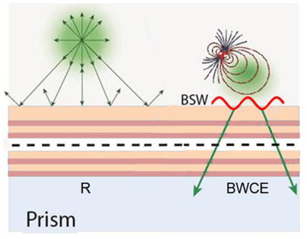
Schematic of fluorophore interactions with a 1DPC. Depending on conditions, the emission can be reflected (R), or coupled with BSWs (BWCE).
To date reports on 1DPCs which display BSWs have been limited to the longer wavelength fluorophores with absorption and emission above 500 nm,27–31 which allows their use with many of the fluorophores used for biomedical research and testing. However, it would be valuable to extend the range to the UV for use with shorter wavelength fluorophores. As an example, the enzyme co-factor NADH absorbs and emits near 350 and 450 nm, respectively. For intrinsic protein fluorescence from tryptophan residues the excitation and emission wavelengths are near 280 and 340 nm, respectively. To the best of our knowledge 1DPCs which display BSW modes for these wavelength region have not been reported. In the present paper we describe a 1DPC that display BSWs at wavelengths ranging from 280 to 440 nm.
Experimental Methods
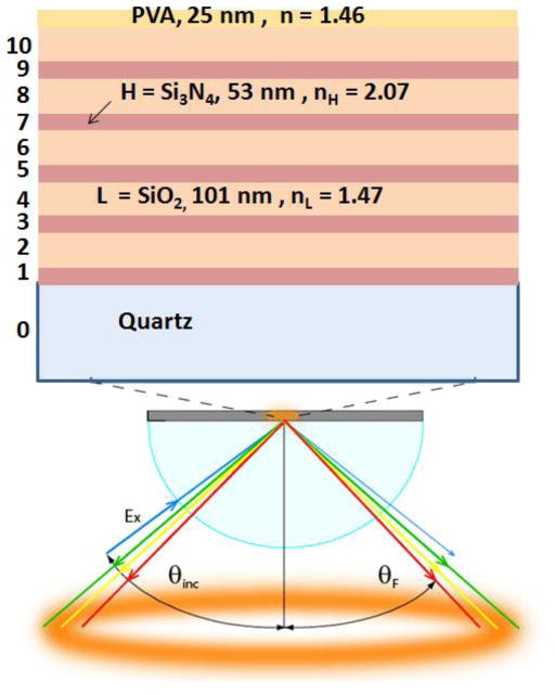
The BSW structure was made by plasma-enhanced chemical vapor deposition on quartz slides. The slide was coated with alternating layers of silicon nitride (Si3N4) and silica (SiO2). Si3N4 was the high (H) dielectric constant component with a refractive index (n) of about 2.07 at 380 nm. Silica was the low (L) dielectric component with n = 1.47 for the same wavelength. These values were determined using spectroscopic N-and-K analyzer using control samples of a silicon wafer coated with a single layer of Si3N4 or silica.27 This initial structure had five layers each of Si3N4 and silica (H5L5). These dielectrics were selected because of their lack of absorbance in our experimental range above 280 nm. The thicknesses of the H and L layers and of the top PVA layer were selected by simulations of the transmission and reflectance spectra using the TFCalc program from Software Spectra, Inc. Simulations of dipole fields and radiation patterns were performed using software from Lumerical, Inc. or Comsol Multiphysics, as indicated in text. The structure was then spin coated with 2-aminopurine (2-AP) and polyvinyl alcohol (PVA) dissolved in water to obtain a top layer of 25 nm thick PVA.
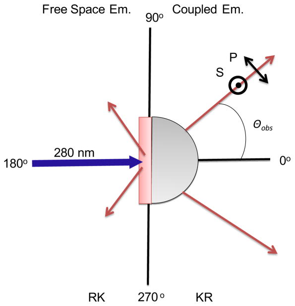
Fluorescence measurements were performed using the home-built apparatus. The schematic of experimental geometry used for the present study is shown in Figure 2. The BSW structure was mounted on a cylindrical prism using glycerol as an index matching fluid. From the top side of the sample, with the PVA layer, 280 nm light from an LED source was used to illuminate 2-AP. The 280 nm excitation was presumed to be unpolarized. A 320 nm long-pass filter is used to eliminate the excitation light and other wavelengths from the LED source. The emission was collected with a 1 mm diameter fiber positioned about 2 cm from the prism, and then measured with a SD2000 Ocean Optics spectrometer. The input of the fiber was rotated around the out-of-plane axis in Figure 2. The air side of the sample is called reverse Kretschmann (RK) or free-space (FS). The prism side is called the Kretschmann (KR) side or configuration.
Figure 2.
Experimental geometry and polarization used with the 1DPC.
Results and Discussions
Design and Optical Properties of the BSW Structure
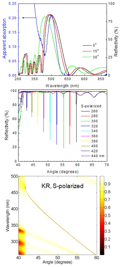
We used simulations to obtain the dielectric layer thickness for a photonic band gap (PBG) which overlaps with the absorption and emission maximum of 2-AP. Not all 1DPCs support BSWs and we did not find publications on a 1DPC structure for wavelengths shorter than 500 nm. Our structure (Figure 3) displays BSWs starting at 280 nm (Figure 4, middle). The larger dielectric layer thickness of the combined silica-PVA top layer of 126 nm was necessary to obtain a BSW resonance. 1DPC structures without a different top layer thickness often do not display BSWs. Simulated absorption spectra showed a photonic band gap near 500 nm for light incident at 0° (Figure 4, top). The oscillations in the simulated spectra are known to be due to the limited number of H and L layers.41–42 This spectrum shifts to shorter wavelengths as the incident angle is changed from 0° to 15° or to 30°. The measured apparent absorption spectrum of the fabricated BSW structure has an absorption maximum near 490 nm (Figure 4, top) which is ascribed to the PBG and is consistent with the simulations. We use the term apparent absorption because the measured spectra reveal the fraction of the incident light which passes through the structure. Light which is reflected or scattered is seen as absorbance. The measured absorption spectrum shows increased absorption below 370 nm. Based on the known optical constants this absorption is not due to pure SiO2 or Si3N4. At this time we do not know the origin of the increased absorption of the 1DPC below 370 nm.
Figure 3.
Schematic of a 1DPC structure on a hemispherical prism and coupled emission. The upper panel shows the structure of BSW structure. For all simulations we used the real (n) and imaginary (κ) parts of refractive index at 380 nm. The values are: nL = 1.47, κL = 4x10⁻⁵ for SiO2, nH = 2.08, κH = 3x10⁻⁴ for Si3N4 and nPVA = 1.46, κPVA = 1x10⁻⁵ for PVA. More details are reported previously (Reference 27).
Figure 4.
Calculated reflectivity spectra (top) and S-polarized angle dependent reflectivity (middle) of the BSW structure shown in Figure 3. The blue line in top panel shows the experimental apparent absorption spectrum for this structure. Dispersion diagram for the 1DPC that shows the reflectivity for a range of wavelengths and incidence angles (bottom).
The middle panel of Figure 4 shows the simulated angle-dependent reflectivity of the BSW structure at incident angles above the critical angle. A series of sharp resonances for wavelengths from 260 to 440 nm were found for S-polarized incident light. No such resonances were found for P-polarized light (not shown). Narrow S-polarized resonances are characteristic of BSWs. Without optical losses the BSWs are infinitely narrow. These resonances can be missed in the simulated absorption because smaller steps in wavelengths are needed to detect the BSWs. It was necessary to include a small imaginary component to the complex refractive index to simulate losses and to detect the BSWs. The details on the imaginary components are mentioned in Figure 3 legend, and in Ref 27. The alternative approach of representing the BSW reflectivity from the structure is shown in Figure 4 bottom. These dispersion diagrams are often used frequency (energy) vs wavevector axes. Herein we used wavelength versus incident angle axes which are more directly connected to the experimental results. The dark yellow shade in the dispersion indicates a decrease in reflectivity and the presence of an optical mode. The width and strength of the mode can be judged by the width and darkness of the shading. The regions in these two panels are due to coupling of the S-polarized incident light into the structure. Increase in the angle of incidence result in a blue-shift in the resonating wavelength. These decreases in reflectivity are due to coupling of incident light to the Bloch surface waves. The weaker bands at shorter wavelengths are due to coupling to internal modes in the 1DPC.
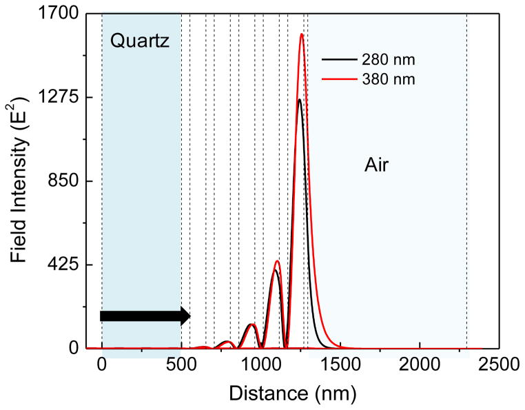
The simulated spectra shown in Figure 4 demonstrate that there is a BSW resonance in the structure but does not show that the electric fields are localized at the surface. Figure 5 shows the simulated field intensity (E2) for light incident through the prism at the BSW resonance angles. The field intensity is localized in the top layer of the dielectric with a high intensity in the PVA layer and high evanescent fields beyond the PVA-air interface. The average fields in the top PVA layer are over 800-fold higher relative to the incident light for 280 nm, and are still higher for 380 nm. These highly increased fields are due to the low optical losses in the dielectrics. For comparison, the fields above a 40 nm thin silver film, used for surface plasmon resonance at longer wavelengths, are enhanced about 20-, and 15- fold for 280 and 380 nm, respectively. The lower fields above an Ag film are due to the losses in the metal,45–46 which rapidly dissipates optical energy. The BSW fields are also much higher than those obtained with total internal reflection (TIR), which are typically 2 to 3-fold.
Figure 5.
Calculated electric field intensities (E2) for the BSW angles using 280 and 380 nm wavelength illumination through an index-matching prism. The incident angles were chosen to match the resonances in Figure 4. The fields are relative to the incident light intensity.
Emission of 2-AP on the BSW Structure
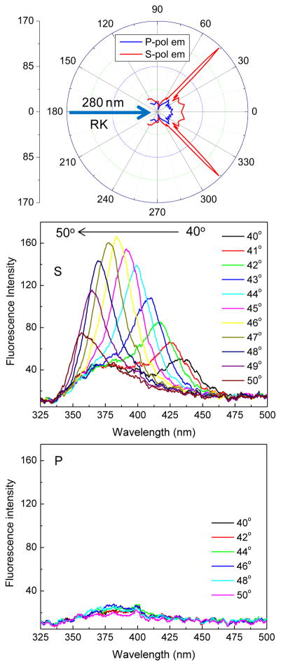
Coupling of fluorophores to thin metal films results in a cone of emission appearing at a well-defined angle from the normal axis.11–13 The BSW structure, with the 2-AP-PVA coating, was refractive index matched with a cylindrical prism. The excitation light from a 280 nm LED was incident normal to the surface (180°) from the sample (RK) direction (Figure 2). With these optical conditions the incident light can excite the entire thickness of the PVA layer, and not just the fluorophores close to the BSW surface. This mode of excitation does not create BSWs at the incident wavelength and does not take advantage of the enhanced fields obtained with KR incidence (Figure 5). Even with these unfavorable conditions there was strong S-polarized emission at an angle 46° from the normal on the KR side of the structure (Figure 6). The middle panel shows emission spectra recorded at angles from 40 to 50°. The emission maximum was strongly dependent on the observation angle and shifted to shorter wavelengths at larger angles. The recorded emission spectra were also more narrow than that of 2-AP without a nearby photonic structure, which has a similar shape to the lower area not covered by the traces. With the emission polarizer at the P-orientation the emission intensities were close to zero (Figure 6, bottom panel) showing that the emission coupled through the BSW structure is almost 100% S-polarized.
Figure 6.
Angular distribution of 2-AP emission intensity at 380 nm (top). S-polarized (middle) and P-polarized (bottom) emission spectra of 2-AP in 1%PVA on BSW. RK illumination using 280 nm LED.
Simulations for 2-AP on the BSW Structure
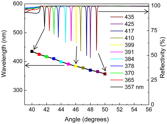
We compared the emission maxima from Figure 6 (top) with simulated BSW resonances at these same wavelengths (Figure 7). These emission maxima and simulated resonances both shift to shorter wavelengths at higher angles. The angular spread of the emission maxima is somewhat larger for the measured values as compared to the simulated resonances. Some of the differences in the experimental versus calculated values are due to the maxima being weighted by the emission spectral shape of 2AP. It should be noted that the comparison of the calculated and experimental values is done without any fitted parameters. The angular distribution of the emission, the S-polarization and the dependence of the emission maxima on the observation angle demonstrate that Bloch wave coupled emission is occurring with the BSW structure.
Figure 7.
Measured angle-dependent emission maximum of 2-AP (squares) from the BSW structure and the simulated reflectivities at the same wavelengths.
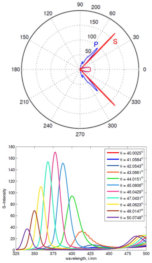
The reflectivity simulations in Figure 4 are for plane-wave illumination from the far-field. We questioned if similar wavelengths and angle-dependent properties occur for a fluorophore (dipole) within a near-field distance from the BSW structure. Comsol Multiphysics was used to simulate a 380 nm dipole positioned in the PVA at 5 nm from the top silica layer with a random dipole orientation relative to the surface. The simulated coupled emission at 380 nm occurred at an angle of 45° (Figure 8, top), which is in excellent agreement with the observed values. The coupled emission was found to show higher intensity for S- as compared to P-polarization. The amount of simulated P-polarized emission seems to be relatively larger than the observed values (Figure 6). This effect is probably due to the short 5 nm distance of the simulated dipole as compared to the 25 nm thick PVA film used for the experiments. Electrodynamic simulations were also performed for wavelengths across the emission spectrum of 2-AP. When the intensities were scaled by the shape of the 2-AP emission spectrum the simulated angle-dependent spectra (Figure 8, bottom) are closely comparable to the observed angle-dependent spectra (Figure 6). The larger widths of the observed angle-dependent spectra are probably the result of imperfections in the fabricated structures as compared to the simulated structure which does not have imperfections.
Figure 8.
Simulated emission intensity distribution for 380 nm dipole positioned in PVA 5 nm above the BSW structure (Top) and far-field angle-dependent S-polarized emission coupling to the BSW structure (Bottom). These finite-difference time-domain (FDTD) simulations were performed using a script for Comsol Metaphysics.
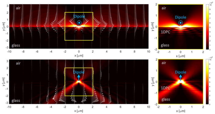
Additional insight into BWCE was obtained by electrodynamic simulations of the electric fields created by a dipole near the structure. A Finite Element Model (FEM) has been set up consisting in a two-dimensional cross-section of the multilayer, as viewed laterally. The multilayer is contacted to a lower semi-infinite domain made of glass (n=1.5) and an upper semi-infinite domain consisting of air (m = 1.0). The |E|2 field and the Poynting vector distribution associated to the radiation emitted by an ideal dipole at 420 nm wavelength are calculated, wherein the dipole is embedded into the PVA layer and located 5 nm from the surface. Two dipole orientations are considered: vertical orientation (perpendicular to the multilayer surface) and horizontal orientation (parallel to the multilayer surface). The |E| 2 distribution is rendered in linear colorscale and the Poynting vector is illustrated as a superposed arrow plot. The arrow length is proportional to the local value of the Poynting vector, in logarithmic scale. The vertical dipole gives rise to a P-polarized radiation, whilst the horizontal dipole gives rise to a purely S-polarized radiation in the plane. In Figure 9 (top panel) the horizontal dipole is considered. By observing the field distribution over a large area, it is found that the S-polarized emission significantly couples to the S-polarized BSW mode sustained by the multilayer. This observation is supported by the presence of a strong field enhancement at the top multilayer surface (see zoomed image on the right-top panel). The distribution of the Poynting vector suggests that the emitted power delivered to the BSW is propagated far away from the dipole according the narrow width of the BSW resonance. For light incident through a prism at the BSW resonance angle, the |E|2 fields are located mostly within the structure (Figure 9). In contrast, the dipole-induced |E|2 field exists mostly above the structure (Figure 9). During propagation, some radiation leakage occurs, which will results in a far-field BSWCE as detected experimentally. The BSW surface distribution does not affect our measurements which are for an area above 1 mm in diameter. Conversely, a vertically oriented dipole emitting P-polarized radiation does not show any coupling to the BSW (see Fig. 9 bottom panel), as expected because of the polarization mismatch.
Figure 9.
Numerical FEM model of the |E|2 (false color map) and Poynting vector (arrow plot) distributions of the radiation emitted by a dipole embedded within a PVA layer, at 5 nm from the 1DPC surface. Dipole with horizontal orientation showing S-polarized emission coupled to BSW is shown in the top panel. Dipole with vertical orientation showing P-polarized emission with no coupling to BSW is shown in the bottom panel. Emission wavelength is 420 nm. Calculations are performed using Comsol Multiphysics software. Color scale for |E| 2 is linear. Arrow length is proportional to Poynting vector on a logarithmic scale.
Conclusion
These results demonstrate that the BWCE can occur with UV excitation and emission ranging from 350 nm in the UV to 450 nm with a BSW structure. There is close agreement between simulations of the optical properties of the BSW with the emission angles and emission wavelength. This agreement shows that electrodynamic simulations can be used to design BSW structures for fluorophores with different absorption and emission spectra. The present BSW structure is robust to handling and can be washed and reused for multiple experiments.
BSW structures have physical and optical properties which are favorable for use at the bedside or for self-testing. For example, the spectra in Figure 6 show that the BSW structure effectively collected the emission and provided angular separation of wavelengths. This suggests the use of 1DPC and BSW structures in portable optical devices which are now appearing with cell phones.47–49 The angular separation of wavelengths by the BSW structure provides a potential for multi-wavelengths or multiplex assays for use in genomics and protein arrays.50 It appears likely that the use of near-field effects and less use of freely propagating light, will incorporated into the next generation of applied optical devices.
Acknowledgments
This work was supported by grants JRL from the National Institute of Health, EB018959, GM107986, EB006521, and S10OD019975. This work was also supported by the NSF MRSEC program at the University of Utah under grant No. DMR1121252. Additional support was provided by the National Key Basic Research Program of China under grant nos. 2013CBA01703, 2012CB922003, the National Natural Science Foundation of China under grant nos. 61427818, 11374286, Science and Technological Fund of Anhui Province for Outstanding Youth (1608085J02). The authors thank Dr. Junxue Chen from the Southwest University of Science and Technology, Mianyang, Sichuan, for preliminary simulations.
Footnotes
References
- 1.Lakowicz JR, Ray K, Chowdhury M, Szmacinski H, Fu Y, Zhang J, Nowaczyk K. Plasmon-Controlled Fluorescence: A New Paradigm in Fluorescence Spectroscopy. Analyst. 2008;133:1308–1346. doi: 10.1039/b802918k. [DOI] [PMC free article] [PubMed] [Google Scholar]
- 2.Deng W, Goldys EM. Plasmonic Approach to Enhanced Fluorescence for Applications in Biotechnology and the Life Sciences. Langmuir. 2012;28:10152–10163. doi: 10.1021/la300332x. [DOI] [PubMed] [Google Scholar]
- 3.Demchenko AP. Nanoparticles and Nanocomposites for Fluorescence Sensing and Imaging. Methods Appl Fluoresc. 2013;1:022001–020029. doi: 10.1088/2050-6120/1/2/022001. [DOI] [PubMed] [Google Scholar]
- 4.Whitesides GM. A Glimpse into the Future of Diagnostics. Clin Chem. 2013;59:589–591. doi: 10.1373/clinchem.2013.204347. [DOI] [PubMed] [Google Scholar]
- 5.Rogers ML, Boutelle MG. Real-Time Clinical Monitoring of Biomolecules. Annu Rev Anal Chem. 2013;6:427–453. doi: 10.1146/annurev.anchem.111808.073648. [DOI] [PubMed] [Google Scholar]
- 6.Gonzalez-Gonzalez M, Jara-Acevedo R, Matarraz S, Jara-Acevedo M, Paradinas S, Sayagules JM, Orfao A, Fuentes M. Nanotechniques in Proteomics: Protein Microarrays and Novel Detection Platforms. Eur J Pharm Sci. 2012;45:499–506. doi: 10.1016/j.ejps.2011.07.009. [DOI] [PubMed] [Google Scholar]
- 7.Rich R, Li J, Fudala R, Gryczynski Z, Gryczynski I, Mandeci W. Properties of Coatings on RFID P-Chips that Support Plasmonic Fluorescence Enhancement in Bioassays. Anal Bioanal Chem. 2012;404:2223–2231. doi: 10.1007/s00216-012-6369-9. [DOI] [PMC free article] [PubMed] [Google Scholar]
- 8.Kozma P, Lehmann A, Wunderlich K, Michel D, Schumacher S, Ehrentreich-Forster E, Bier FF. A Novel Handheld Fluorescent Microarray Reader for Point-of-Care Diagnostic. Biosensors and Bioelectron. 2013;47:415–420. doi: 10.1016/j.bios.2013.03.043. [DOI] [PubMed] [Google Scholar]
- 9.Kovarik ML, Jacobson SC. Nanlfuidics in Lab-On-A-Chip Devices. Anal Chem. 2009;81:7133–7140. doi: 10.1021/ac900614k. [DOI] [PubMed] [Google Scholar]
- 10.Lakowicz JR. Radiative Decay Engineering 3. Surface Plasmon-Coupled Directional Emission. Anal Biochem. 2004;324:153–169. doi: 10.1016/j.ab.2003.09.039. [DOI] [PMC free article] [PubMed] [Google Scholar]
- 11.Gryczynski I, Malicka J, Gryczynski Z, Lakowicz JR. Radiative Decay Engineering 4. Experimental Studies of Surface Plasmon-Coupled Directional Emission. Anal Biochem. 2004;324:170–182. doi: 10.1016/j.ab.2003.09.036. [DOI] [PMC free article] [PubMed] [Google Scholar]
- 12.Calander N. Surface Plasmon-Coupled Emission and Fabry-Perot Resonance in the Sample Layer: A Theoretical Approach. J Phys Chem B. 2005;109:13957–13963. doi: 10.1021/jp0510544. [DOI] [PubMed] [Google Scholar]
- 13.Choudhury SD, Badugu R, Lakowicz JR. Directing Fluorescence with Plasmonic and Photonic Structures. Acc Chem Res. 2015;48:2171–2180. doi: 10.1021/acs.accounts.5b00100. [DOI] [PMC free article] [PubMed] [Google Scholar]
- 14.Ganguly M, Mondal C, Chowdhury J, Pal J, Pal A, Pal T. The Tuning of Metal Enhanced Fluorescence for Sensing Applications. Dalton Trans. 2013;43:1032–1047. doi: 10.1039/c3dt52258j. [DOI] [PubMed] [Google Scholar]
- 15.Giannini V, Fernandez-Dominguez AI, Heck SC, Maier SA. Plasmonic Nanoantennas: Fundamentals and Their Use in Controlling the Radiative Properties of Nanoemitters. Chem Rev. 2011;111:3888–3912. doi: 10.1021/cr1002672. [DOI] [PubMed] [Google Scholar]
- 16.Knight MW, Liu L, Wang Y, Brown L, Mukherjee S, King NS, Everitt HO, Nordlander P, Halas NJ. Aluminum Plasmonic Nanoantennas. Nano Lett. 2012;12:6000–6004. doi: 10.1021/nl303517v. [DOI] [PubMed] [Google Scholar]
- 17.Knight MW, King NS, Liu L, Everitt HO, Nordlander P, Halas NJ. Aluminum for Plasmonics. ACS Nano. 2014;8:834–840. doi: 10.1021/nn405495q. [DOI] [PubMed] [Google Scholar]
- 18.Ross MB, Schatz GC. Aluminum and Indium Plasmonic Nanoantennas in the Ultraviolet. J Phys Chem C. 2014;118:12506–12514. [Google Scholar]
- 19.Chowdhury MH, Ray K, Gray SK, Pond J, Lakowicz JR. Aluminum Nanoparticles as Substrates for Metal-Enhanced Fluorescence in the Ultraviolet for the Label-Free Detection of Biomolecules. Anal Chem. 2009;81:1397–1403. doi: 10.1021/ac802118s. [DOI] [PMC free article] [PubMed] [Google Scholar]
- 20.Malicka J, Gryczynski I, Gryczynski Z, Lakowicz JR. Surface Plasmon-Coupled Ultraviolet Emission of 2,5-Diphenyl-1,3,4-oxadiazole. J Phys Chem B. 2004;108:19114–19118. doi: 10.1021/jp047136u. [DOI] [PMC free article] [PubMed] [Google Scholar]
- 21.Gryczynski I, Malicka J, Gryczynski Z, Nowaczyk K, Lakowicz JR. Ultraviolet Surface Plasmon-Coupled Emission Using Thin Aluminum Films. Anal Chem. 2004;76:4076–4081. doi: 10.1021/ac040004c. [DOI] [PMC free article] [PubMed] [Google Scholar]
- 22.Forestiere C, Handin A, Dal Negro L. Enhancement of Molecular Fluorescence in the UV Spectral Range Using Aluminum Nanoantennas. Plasmonics. 2014;9:715–725. [Google Scholar]
- 23.Dragan AI, Geddes CD. Indium Nanodeposits: A Substrate for Metal-Enhanced Fluorescence in the Ultraviolet Spectral Region. J Appl Phys. 2010;108:094701-1–7. [Google Scholar]
- 24.Guo JH, Liu LZ, Zhu XB, Wu XL, Chu PK. Enhanced Fluorescence from Dye Molecules by Au Nanoparticles on Asymmetric Double-stranded DNA and Mechanism. Appl Phys Letts. 2014;104:141910-1–3. [Google Scholar]
- 25.Wang J, Achilefu S, Nantz M, Kang KA. Gold Nanoparticle-Fluorophore Complex for Conditionally Fluorescing Signal Mediator. Anal Chim Acta. 2011;695:96–104. doi: 10.1016/j.aca.2011.03.058. [DOI] [PubMed] [Google Scholar]
- 26.Yang B, Lu N, Qi D, Ma R, Wu Q, Hao J, Liu X, Mu Y, Reboud V, Kehagias N, et al. Tuning the Intensity of Metal-Enhanced Fluorescence by Engineering Silver Nanoparticle Arrays. Small. 2010;6:1038–1043. doi: 10.1002/smll.200902350. [DOI] [PubMed] [Google Scholar]
- 27.Badugu R, Nowaczyk K, Descrovi E, Lakowicz JR. Radiative Decay Engineering 6: Fluorescence on One-Dimensional Photonic Crystals. Anal Biochem. 2013;442:83–96. doi: 10.1016/j.ab.2013.07.021. [DOI] [PMC free article] [PubMed] [Google Scholar]
- 28.Han L, Zhang D, Chen Y, Wang R, Zhu L, Wang P, Ming H, Badugu R, Lakowicz JR. Polymer-Loaded Propagating Modes on a One-Dimensional Photonic Crystal. Appl Phys Letts. 2014;104:061115-1–6. doi: 10.1063/1.4865421. [DOI] [PMC free article] [PubMed] [Google Scholar]
- 29.Zhang D, Badugu R, Chen Y, Yu S, Yao P, Wang P, Ming H, Lakowicz JR. Back Focal Plane Imaging of Directional Emission from Dye Molecules Coupled to One-Dimensional Photonic Crystals. Nanotechnology. 2014;25:145202-1–10. doi: 10.1088/0957-4484/25/14/145202. [DOI] [PMC free article] [PubMed] [Google Scholar]
- 30.Liscidini M, Galli M, Shi M, Dacarro G, Patrini M, Bajoni D, Sipe JE. Strong Modification of Light Emission from a Dye Monolayer via Bloch Surface Waves. Optics Letts. 2009;34:2381–2320. doi: 10.1364/ol.34.002318. [DOI] [PubMed] [Google Scholar]
- 31.Ballarini M, Frascella F, Michelotti F, Digregorio G, Rivolo P, Paeder V, Musi V, Giorgis F, Descrovi E. Bloch Surface Waves-Controlled Emission of Organic Dyes Grafted on a One-Dimensional Photonic Crystal. Appl Phys Letts. 2011;99:043302-1–3. [Google Scholar]
- 32.Soboleva IV, Descrovi E, Summonte C, Fedyanin AA, Giorgis F. Fluorescence Emission Enhanced by Surface Electromagnetic Waves on One-Dimensional Photonic Crystals. Appl Phys Letts. 2009;94:231122-1–3. [Google Scholar]
- 33.Frascella F, Ricciardi S, Rivolo P, Moi V, Michelotti F, Munzert P, Danz N, Napione L, Alvaro M, Giorgis F, et al. A Fluorescent One-Dimensional Photonic Crystal for Label-Free Biosensing Based on Bloch Surface Waves. Sensors. 2013;13:2011–2022. doi: 10.3390/s130202011. [DOI] [PMC free article] [PubMed] [Google Scholar]
- 34.Sinibaldi A, Fieramosca A, Rizzo R, Anopchenko A, Danz N, Munzert P, Magistris C, Barolo C, Michelotti F. Combining Label-Free and Fluorescence Operation of Bloch Surface Wave Optical Sensors. Opt Letts. 2014;39:2947–2950. doi: 10.1364/OL.39.002947. [DOI] [PubMed] [Google Scholar]
- 35.Lodahi P, van Driel F, Nikolaev IS, Irman A, Overgaag K, Vanmaekelbergh D, Vos WL. Controlling the Dynamics of Spontaneous Emission from Quantum Dots by Photonic Crystals. Nature. 2004;430:654–657. doi: 10.1038/nature02772. [DOI] [PubMed] [Google Scholar]
- 36.Ganesh N, Zhang W, Mathias PC, Chow E, Soares JANT, Malyarchuk V, Smith AD, Cunningham BT. Enhanced Fluorescence Emission from Quantum Dots on a Photonic Crystal Surface. Nature Nanotechnology. 2007;3:515–520. doi: 10.1038/nnano.2007.216. [DOI] [PubMed] [Google Scholar]
- 37.Nikolaev IS, Lodahl P, Vos WL. Fluorescence Lifetime of Emitters with Broad Homogeneous Linewidths Modified in Opal Photonic Crystals. J Phys Chem C. 2008;112:7250–7254. [Google Scholar]
- 38.Chaudhery V, Lu M, Huang CS, Polans J, Tan R, Zangar RC, Cunningham BT. Line-Scanning Detection Instrument for Photonic Crystal Enhanced Fluorescence. Optics Letts. 2012;37:2565–2567. doi: 10.1364/OL.37.002565. [DOI] [PubMed] [Google Scholar]
- 39.Block ID, Mathias PC, Ganesh N, Jones SL, Dorvel BR, Chaudhery V, Vodkin LO, Bashir R, Cunningham BT. A Detection Instrument for Enhanced-Fluorescence and Label-Free Imaging on Photonic Crystal Surfaces. Optics Exp. 2009;17:13222–13235. doi: 10.1364/oe.17.013222. [DOI] [PMC free article] [PubMed] [Google Scholar]
- 40.Huang CS, George S, Lu M, Chaudhery V, Tan R, Zangar RC, Cunningham BT. Application of Photonic Crystal Enhanced Fluorescence to Cancer Biomarker Microarrays. Anal Chem. 2011;83:1425–1430. doi: 10.1021/ac102989n. [DOI] [PMC free article] [PubMed] [Google Scholar]
- 41.Saleh BEA, Teich MC. Fundamentals of Photonics. 2. Wiley-Interscience; 2007. p. 1177. [Google Scholar]
- 42.Joannopoulos JD, Johnson SG, Winn JN, Meade RD. Photonic Crystals Molding the Flow of Light. 2. Princeton University Press; 2008. p. 286. [Google Scholar]
- 43.Ramos-Mendieta F, Halevi P. Surface Electromagnetic Waves in Two-Dimensional Photonic Crystals: Effect of the Position of the Surface Plane. Phys Rev B. 1999;59:15112–15120. [Google Scholar]
- 44.Maede RD, Brommer KD, Rappe AM, Joannopoulos JD. Electromagnetic Bloch Waves at the Surface of a Photonic Crystal. Phys Rev B. 1999;44:44–49. doi: 10.1103/physrevb.44.10961. [DOI] [PubMed] [Google Scholar]
- 45.Homola J. Surface Plasmon Resonance Sensors for Detection of Chemical and Biological Species. Chem Rev. 2008;108:462–493. doi: 10.1021/cr068107d. [DOI] [PubMed] [Google Scholar]
- 46.Tanious FA, Nguyen B, Wilson WD. Biosensor-Surface Plasmon Resonance Methods for Quantitative Analysis of Biomolecular Interactions. Methods in Cell Biology. 2008;84:53–77. doi: 10.1016/S0091-679X(07)84003-9. [DOI] [PubMed] [Google Scholar]
- 47.Ayas S, Cupallari A, Ekiz OO, Kaya Y, Dana A. Counting Molecules with a Mobile Phone Camera Using Plasmonic Enhancement. ACS Photonics. 2014;1:17–26. [Google Scholar]
- 48.Canning J, Lau A, Naqshbandi M, Petermann I, Crossley MJ. Measurement of Fluorescence in a Rhodamine-123 Doped Self-Assembled AGiant@ Mesostructured Silica Sphere Using a Smartphone as Optical Hardware. Sensors. 2011;11:7055–7062. doi: 10.3390/s110707055. [DOI] [PMC free article] [PubMed] [Google Scholar]
- 49.Smith ZJ, Chu K, Espenson AR, Rahimzadeh M, Gryshuk A, Molinaro M, Dwyre DM, Lane S, Matthews D, Wachsmann-Hogiu S. Cell-Phone-Based Platform for Biomedical Device Development and Education Applications. PloS One. 2011;6:e17150-1–4. doi: 10.1371/journal.pone.0017150. [DOI] [PMC free article] [PubMed] [Google Scholar]
- 50.Templin MF, Stoll D, Schrenk M, Traub PC, Vohringer CF, Joos TO. Protein Microarray Technology. Trends in Biotechnol. 2002;20:160–166. doi: 10.1016/s0167-7799(01)01910-2. [DOI] [PubMed] [Google Scholar]
- 51.Niedringhaus TP, Milanova D, Kerby MB, Snyder MP, Barron AE. Landscape of Next-Generation Sequencing Technologies. Anal Chem. 2011;83:4327–4341. doi: 10.1021/ac2010857. [DOI] [PMC free article] [PubMed] [Google Scholar]
- 52.Hecht J. Advances in Photonics-Based Tools Expand Genomics Possibilities. Clin Chem. 2013;59:49–52. [Google Scholar]


