Abstract
We report on the significant performance enhancement of SnO2 thin film ultraviolet (UV) photodetectors (PDs) through incorporation of CuO/SnO2 p-n nanoscale heterojunctions. The nanoheterojunctions are self-assembled by sputtering Cu clusters that oxidize in ambient to form CuO. We attribute the performance improvements to enhanced UV absorption, demonstrated both experimentally and using optical simulations, and electron transfer facilitated by the nanoheterojunctions. The peak responsivity of the PDs at a bias of 0.2 V improved from 1.9 A/W in a SnO2-only device to 10.3 A/W after CuO deposition. The wavelength-dependent photocurrent-to-dark current ratio was estimated to be ~ 592 for the CuO/SnO2 PD at 290 nm. The morphology, distribution of nanoparticles, and optical properties of the CuO/SnO2 heterostructured thin films are also investigated.
Transparent oxide semiconductors (TOSs) have attracted considerable attention in recent years, due to their versatile applications in transparent thin-film transistors,1,2 transparent electrodes,3 and optoelectronics4–6. Visible-blind ultraviolet (UV) photodetectors (PDs) are of particular interest, owing to their broad application in digital imaging, missile plume detection, optical communications, and biomedical sensing.7–9 Due to its wide bandgap and consequent transparency in the visible spectral region, SnO2 has been demonstrated as a useful material for visible-blind UV photon detection.10–12
Typical n-SnO2 PDs work as photoconductors with electrons as the majority carriers. In a photoconductor, absorption of photons with energy larger than the bandgap energy generates free carriers, leading to an increase in conductivity for a period known as the persistence time. The device conducts a single carrier type, and the persistence time can be lengthened by trapping of the non-conducting carrier type, leading to photoconductive gain and quantum efficiency of greater than 100%. At a specific operation bias, the photocurrent is measured as the response of the PD, which can be used to calculate the EQE (external quantum efficiency) and responsivity of the device.
Current SnO2 thin-film PD technology is limited by low responsivity, especially at longer UV wavelengths.13 Efforts to improve device performance have focused on achieving better crystal quality and building one-dimensional SnO2 nanostructures.9,14–16 The reported ultrahigh responsivity14 of SnO2 based PDs indicates that SnO2 is a promising material for high-performing PDs. Here, we build thin-film SnO2 PDs using a novel, facile, and scalable approach to fabricate nanoscale p-n heterojunctions with enhanced light absorption in the active material to improve the performance of UV PDs.
Nanorod-based heterojunctions consisting of p-CuO and n-SnO2 have been previously developed for applications such as gas sensors.17,18 Our simplified PD device fabrication method consists of using rf-sputtering to deposit SnO2 thin films and Cu nanoparticle (NP) clusters. The top layer of Cu NPs oxidizes in ambient to form CuO NP clusters, and the primary role of these clusters is to enhance absorption at the longer wavelength edge of the UV response in the PDs. We used finite-difference time-domain (FDTD) simulations to model the light absorption in devices with and without the CuO NPs and achieved good agreement with the experimental absorption spectra. Our electrical measurements indicated that the inclusion of the CuO NPs improved the responsivity of the PDs more than 5 fold compared to SnO2-only devices.
The SnO2 thin films were rf-sputtered using a SnO2 target on sapphire substrates in a Denton** Vacuum Discovery 550 sputtering system. The base pressure was kept at or below 6.7 × 10⁻⁴ Pa (5 × 10⁻⁶ Torr), and the substrate temperature was maintained at 325 °C to yield uniform films. The thickness of the deposited SnO2 was measured using a J. A. Woollam M2000 ellipsometer and estimated to be (95 ± 2) nm.
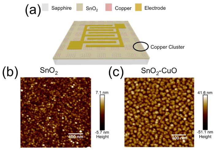
The Cu NP clusters were deposited on the SnO2 films by rf-sputtering at room temperature. The deposition time was 185 seconds, and a shadow mask was used to form square-shaped clusters composed of self-assembled nanoparticles with a nominal height of 40–50 nm rather than continuous cluster films. The total areal size of the Cu clusters was 200 μm × 200 μm, and they were spaced by 200 μm, as shown in Figure 1(a). Oxidation of the Cu nanoparticles occurred spontaneously during and immediately following the deposition, resulting in the formation of CuO NPs. X-ray photoelectron spectroscopy (XPS) measurements indicated that the final NP clusters are primarily (> 95 %) composed of CuO, as shown in Figure 2(b). Electron beam evaporation was used to deposit Ti/Al/Ti/Au interdigitated electrodes (IDEs) as the final step in the PD fabrication process. Figure 1(a) shows a device schematic of the entire structure.
FIG. 1.
(a) Schematic of a SnO2-CuO nanocluster PD device including the top interdigitated electrodes. Dimensions are not to scale. (b) High-resolution AFM image of an as-deposited SnO2 film. (c) High-resolution AFM image of a SnO2 film with a top layer of CuO nanoclusters.
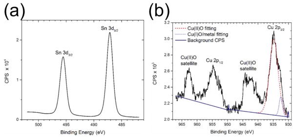
FIG. 2.
High-resolution XPS spectra of (a) the Sn 3d and (b) the Cu 2p regions of a SnO2-CuO film. CPS is counts per second.
The surface morphology of the SnO2 and SnO2-CuO films was measured using a Bruker Dimension FastScan atomic force microscope (AFM). Figures 1(b) and 1(c) show high-resolution AFM images of the bare SnO2 film and the SnO2 with a top layer of self-assembled CuO NPs. The measured root mean square (rms) surface roughness of the bare SnO2 film was 1.8 nm, and the rms value increased to 13.8 nm after the addition of the CuO NPs. The grain sizes of the SnO2 film and the CuO nanoclusters were estimated as (32.9 ± 13) nm and (74.6 ± 25) nm, respectively. A rough statistical analysis performed on the image in Figure 1(c) resulted in an average CuO NP surface density of 65 μm−2 and an average particle height of 45 nm. These estimated parameters were used in the FDTD simulations described below.
We used XPS measurements to confirm the chemical identity of the SnO2-CuO films. XPS curve-fitting and analysis was performed using CasaXPS software. The binding energies of the spectra were calibrated to the hydrocarbon peak at 284.8 eV. High-resolution XPS spectra of the Sn 3d and Cu 2p regions of the SnO2-CuO film are shown in Figures 2(a) and 2(b), respectively. As seen in Figure 2(a), the Sn 3d 5/2 peak appears at a binding energy of (487.1 ± 0.1) eV with a satellite peak characteristic of Sn 3d 3/2 at (495.5 ± 0.1) eV, which is consistent with previously reported XPS data for SnO2.19 The Cu 2p region of the spectrum shows a combination of Cu-related states that can be identified by referring to published reports.20–22 Curve-fitting of the Cu 2p region peaks (Figure 2(b)) was used to estimate that 95 at.% of the Cu content of the sample is in the form of Cu(II)O and the other 5 at.% is in the form of Cu(I)O or Cu metal. From these measurements, we concluded that the deposited Cu NPs are substantially oxidized to form CuO during and after the deposition process.
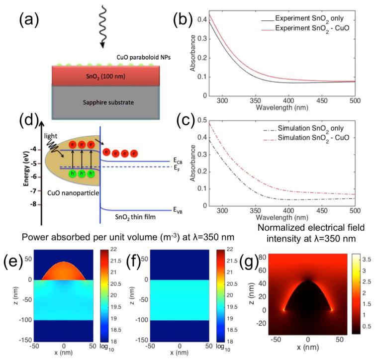
The absorption spectra and absorption coefficients (α) of the SnO2 and SnO2-CuO films were measured using an Ocean Optics QE65000 spectrometer and a J. A. Woollam M2000 ellipsometer, respectively. Optical absorbance spectra of the SnO2 and SnO2-CuO films are shown in Figure 3(b). A significant enhancement in the light absorption over the wavelength range of 250 nm to 475 nm is observed in the film decorated with CuO NPs compared to the bare SnO2 film.
FIG. 3.
(a) Diagram of the setup for the FDTD simulations. A SnO2 film thickness of 100 nm was used for the simulations with and without CuO NPs. The CuO NP clusters were modeled as elliptic paraboloids with heights of 45 nm and diameters of 75 nm. The CuO NPs were randomly distributed on the SnO2 film with an average surface density of 65 μm−2. The size and average density values of the NPs were based on AFM measurements of the real devices. (b) Measured and (c) FDTD simulated absorption spectra of the SnO2 and SnO2-CuO films. (d) Schematic band diagram illustrating the hypothesized electron transfer process in the CuO-SnO2 nanoheterojunctions under irradiation. (e) Spatial cross-section of simulated power absorbed per unit volume at λ = 350 nm in a single CuO NP on a SnO2 film and (f) in a bare SnO2 film. (g) Spatial cross-section of simulated normalized electrical field intensity at λ = 350 nm for a single CuO NP on a SnO2 film.
To verify the enhancement mechanism associated with the addition of the CuO NP clusters, we used FDTD simulations to calculate the optical properties of a 100 nm thick SnO2 film with and without CuO nanoclusters on top. The simulated structure is shown in Figure 3(a). The CuO NPs were modeled as randomly distributed elliptic paraboloids. The particle shape, dimensions and average surface densities were derived from the analysis of the AFM images (Figure 1(c)). Refractive indices for the SnO2 film were obtained from ellipsometry measurements, and reported values were used for the refractive indices for the CuO23 and sapphire24 substrate. A broadband (200 nm – 1000 nm) plane wave incident from the nanocluster side of the device was used as the excitation source for the simulations.
Figures 3(b) and 3(c) show the experimental and simulated absorption spectra for the SnO2 films with and without CuO NP clusters. The simulated and measured spectra show qualitative agreement in the effect of the CuO NPs on the increase in absorbance across all wavelengths in the plotted range, the apparent red shift of the absorption onset, and the change in shape of the absorbance curve. Differences in quantitative agreement can be attributed to inhomogeneity in the NP size and density distributions, and uncertainty in the SnO2 film thickness in the real devices.
The simulated spatial absorption profiles for a single CuO NP on a SnO2 film and a bare SnO2 film at a wavelength of 350 nm are plotted in Figure 3(e) and Figure 3(f). The normalized electrical field intensity at a wavelength 350 nm is plotted in Figure 3(g). There is an enhancement of the local electrical field intensity around the NP and strong associated absorption within the NP. We attribute the enhanced absorption in the composite devices to this effect. Our aim was to use this increase in absorption without relying on an increase in SnO2 film thickness to improve the responsivity of the SnO2-based photodetectors.
A schematic band diagram for the SnO2/CuO pn-nanoheterojunctions is depicted in Figure 3(d) using energy levels reported for p-CuO25 and n-SnO226. The nanoheterojunction structure takes advantage of the intense absorption in the CuO NPs to transfer a high density of photogenerated electrons from the p-CuO NPs to the n-SnO2 film, while the transfer of holes is hindered by the energy barrier at the junction. The smaller bandgap of CuO (1.35 eV25) results in increased absorption at the red edge of the UV spectrum, and the pn-heterojunction nature of the CuO/SnO2 interface facilitates charge transfer upon illumination to increase the responsivity of the photodetector. Electrons injected into the conduction band of SnO2 from the CuO increase the free majority carrier density in the photoconductive material, which could lead to a significant increase in photocurrent in the PD. Although the bandgap of CuO is small, the nanoscale structure of the CuO particles are predicted to allow the films to remain “visible-blind” due to poor in-coupling and low absorption in structures that are much smaller than the visible and infrared material photon absorption lengths.
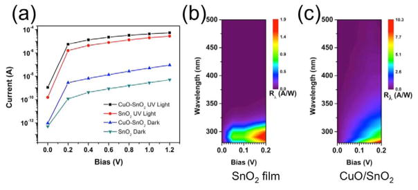
Typical I–V characteristics of the SnO2-only and CuO-SnO2 devices measured in the dark and under UV-illumination are shown in Figure 4(a). The photocurrent generated in the PD with CuO NPs was almost double that of the SnO2-only device under 290 nm wavelength illumination for all tested biases. The measured dark current for the CuO-SnO2 PD was also larger than that of the SnO2-only device, indicating that the conductivity of the CuO-SnO2 composite film was larger than that of the SnO2-only film.
FIG. 4.
(a) ON/OFF I-V curves for SnO2-only and CuO/SnO2 PDs under UV illumination at a wavelength of 290 nm. (b) Responsivity as a function of bias and wavelength for SnO2 and (c) SnO2-CuO thin film photodetecors.
To quantify the performance of the PDs, we used the photocurrent-to-dark current ratio, defined as:
where IUV is the current under UV illumination, and Idark is the dark current at the same voltage. The CuO-SnO2 PDs exhibited a PF of ~ 592 at 1.2 V under 290 nm illumination.
Responsivities of the SnO2 and SnO2-CuO PDs were measured at various bias voltages under a spectrally filtered light source. The measurements, calibrated using a standard NIST silicon photodiode, were associated with a total uncertainty of ± 5 % (fractional). In order to obtain stable and reliable data, the photocurrent at each wavelength was measured with a delay of 180 seconds with respect to the illumination. The need for stable photocurrent operation precluded higher resolution measurements of the PD response time.
The UV photocurrent response of the PDs was recorded over a voltage range of 0 V to 1.2 V at an illumination wavelength of 290 nm, as shown in Figure 4(a). In addition to light current enhancements, the dark current also increases after the SnO2 surface is covered with the CuO NPs, despite the assumed formation of a depletion layer. This increase can be attributed to several potential mechanisms. The small amount of Cu(I)O or Cu metal visible in the XPS spectrum could lead to an increase in the dark current which could be ameliorated in future iterations by including a controlled oxidation step in the fabrication process. Additionally, the presence of defects close to the nanojunction interface could reduce carrier lifetimes, potentially act as dopants, and facilitate leakage paths, contributing to an increase in device dark current.
Figures 4(b) and 4(c) illustrate the spectral responsivity of the SnO2 devices with and without CuO NPs in the low bias regime. The SnO2-only PDs reached a maximum responsivity of 1.9 A/W at 0.2 V bias under 290 nm illumination, while the devices with CuO NP clusters exhibited a responsivity of 10.3 A/W at 0.2 V bias under 280 nm illumination. The incorporation of the CuO NPs resulted in a greater than 5 fold improvement of the responsivity. Additionally, the SnO2-only PD response had a sharp cutoff at around 320 nm in wavelength, whereas the SnO2-CuO PDs displayed some response out to 340 nm in wavelength at low bias. The broadening of the spectral detection range can be attributed to the drastic enhancement of light absorption and charge transfer facilitated by the SnO2-CuO nanoheterojunctions in the UVA spectral region. Although the responsivity of these devices is lower than that of PDs based on one-dimensional structures9,14, it is competitive with thin-film based UV PDs made from other traditional semiconductor materials.27 Additionally, this method produces robust structures without complex fabrication processes that operate at low bias, making it suitable for practical applications.
In summary, we have demonstrated high responsivity visible-blind UV PDs based on sputtered SnO2-CuO nanoheterojunction films. We investigated the properties of the films using AFM and XPS measurements, confirming that the sputtered Cu forms self-assembled nanoparticle clusters that are composed primarily of Cu(II)O after air exposure. The peak responsivity reached a value of 10.3 A/W at a low bias of 0.2 V in the CuO-SnO2 devices, representing a five-fold increase over the highest responsivity achieved in devices without CuO NPs. The performance enhancement is attributed to the intense local absorption of the CuO NPs and the charge transfer facilitated by the CuO-SnO pn nanoheterojunction structures. Our approach of utilizing CuO-based pn nanoheterojunctions to enhance the efficiency of visible-blind SnO2 photodiodes represents a viable path for building UV optoelectronic devices based on cost-effective materials.
Footnotes
Certain commercial equipment, instruments, or materials are identified in this paper in order to specify the experimental procedure adequately. Such identification is not intended to imply recommendation or endorsement by the National Institute of Standards and Technology, nor is it intended to imply that the materials or equipment identified are necessarily the best available for the purpose.
References
- 1.Nomura K, Ohta H, Ueda K, Kamiya T, Hirano M, Hosono H. Science. 2003;300:1269. doi: 10.1126/science.1083212. [DOI] [PubMed] [Google Scholar]
- 2.Nomura K, Ohta H, Takagi A, Kamiya T, Hirano M, Hosono H. Nature. 2004;432:488. doi: 10.1038/nature03090. [DOI] [PubMed] [Google Scholar]
- 3.Minami T. Semicond Sci Technol. 2005;20:S35. [Google Scholar]
- 4.Debnath R, Xie T, Wen B, Li W, Ha JY, Sullivan NF, Nguyen NV, Motayed A. RSC Adv. 2015;5:14646. [Google Scholar]
- 5.Xie T, Liu G, Wen B, Ha JY, Nguyen NV, Motayed A, Debnath R. ACS Appl Mater Interfaces. 2015;7:9660. doi: 10.1021/acsami.5b01420. [DOI] [PubMed] [Google Scholar]
- 6.Xi YY, Hsu YF, Djurišić AB, Ng AMC, Chan WK, Tam HL, Cheah KW. Appl Phys Lett. 2008;92:113505. [Google Scholar]
- 7.Bie YQ, Liao ZM, Zhang HZ, Li GR, Ye Y, Zhou YB, Xu J, Qin ZX, Dai L, Yu DP. Adv Mater. 2011;23:649. doi: 10.1002/adma.201003156. [DOI] [PubMed] [Google Scholar]
- 8.Zhang W, Xu J, Ye W, Li Y, Qi Z, Dai J, Wu Z, Chen C, Yin J, Li J, Jiang H, Fang Y. Appl Phys Lett. 2015;106:021112. [Google Scholar]
- 9.Hu L, Yan J, Liao M, Wu L, Fang X. Small. 2011;7:1012. doi: 10.1002/smll.201002379. [DOI] [PubMed] [Google Scholar]
- 10.Chen Y, Zhu C, Cao M, Wang T. Nanotechnology. 2007;18:285502. [Google Scholar]
- 11.Mathur S, Barth S, Shen H, Pyun JC, Werner U. Small. 2005;1:713. doi: 10.1002/smll.200400168. [DOI] [PubMed] [Google Scholar]
- 12.Chen H, Hu L, Fang X, Wu L. Adv Funct Mater. 2012;22:1229. [Google Scholar]
- 13.Oshima T, Okuno T, Fujita S. Jpn J Appl Phys. 2009;48:120207. [Google Scholar]
- 14.Liu K, Sakurai M, Aono M, Shen D. Adv Funct Mater. 2015;25:3157. [Google Scholar]
- 15.Tian W, Zhang C, Zhai T, Li SL, Wang X, Liao M, Tsukagoshi K, Golberg D, Bando Y. Chem Commun. 2013;49:3739. doi: 10.1039/c3cc39273b. [DOI] [PubMed] [Google Scholar]
- 16.Lin CH, Chen RS, Chen TT, Chen HY, Chen YF, Chen KH, Chen LC. Appl Phys Lett. 2008;93:112115. [Google Scholar]
- 17.Giebelhaus I, Varechkina E, Fischer T, Rumyantseva M, Ivanov V, Gaskov A, Morante JR, Arbiol J, Tyrra W, Mathur S. J Mater Chem A. 2013;1:11261. [Google Scholar]
- 18.Xue X, Xing L, Chen Y, Shi S, Wang Y, Wang T. J Phys Chem C. 2008;112:12157. [Google Scholar]
- 19.Liu L, An M, Yang P, Zhang J. Sci Rep. 2015;5:9055. doi: 10.1038/srep09055. [DOI] [PMC free article] [PubMed] [Google Scholar]
- 20.Vasquez RP. Surf Sci Spectra. 1998;5:262. [Google Scholar]
- 21.Tahir D, Tougaard S. J Phys Condens Matter. 2012;24:175002. doi: 10.1088/0953-8984/24/17/175002. [DOI] [PubMed] [Google Scholar]
- 22.Vasquez RP. Surf Sci Spectra. 1998;5:257. [Google Scholar]
- 23.E.D. Palik, N. Y. 19912, (1991).
- 24.Malitson IH, Dodge MJ. J Opt Soc Am. AMER INST PHYSICS CIRCULATION FULFILLMENT DIV; 500 SUNNYSIDE BLVD, WOODBURY, NY 11797-2999: 1972. pp. 1405–1405. [Google Scholar]
- 25.Koffyberg FP, Benko FA. J Appl Phys. 1982;53:1173. [Google Scholar]
- 26.Robertson J, Xiong K, Clark SJ. Thin Solid Films. 2006;496:1. [Google Scholar]
- 27.Sang L, Liao M, Sumiya M. Sensors. 2013;13:10482. doi: 10.3390/s130810482. [DOI] [PMC free article] [PubMed] [Google Scholar]


