Significance
Bioresorbable electronic systems have the potential to create important new categories of technologies, ranging from temporary biomedical implants to environmentally benign, green consumer devices. The results presented here provide a collection of ideas that establish the foundations for a realistic technology of this type, in which state-of-the-art silicon complementary metal-oxide-semiconductor foundries serve as the source of microscale, water-soluble electronic components configured for rapid assembly and electrical interconnection on soft, biocompatible polymer substrates. Demonstrations in various high-performance electronic systems illustrate the concepts, and fundamental studies establish the chemical kinetics and end products of dissolution in aqueous environments.
Keywords: soft electronics, biodegradable electronics, transfer printing, undercut etching, hydrolysis
Abstract
Foundry-based routes to transient silicon electronic devices have the potential to serve as the manufacturing basis for “green” electronic devices, biodegradable implants, hardware secure data storage systems, and unrecoverable remote devices. This article introduces materials and processing approaches that enable state-of-the-art silicon complementary metal-oxide-semiconductor (CMOS) foundries to be leveraged for high-performance, water-soluble forms of electronics. The key elements are (i) collections of biodegradable electronic materials (e.g., silicon, tungsten, silicon nitride, silicon dioxide) and device architectures that are compatible with manufacturing procedures currently used in the integrated circuit industry, (ii) release schemes and transfer printing methods for integration of multiple ultrathin components formed in this way onto biodegradable polymer substrates, and (iii) planarization and metallization techniques to yield interconnected and fully functional systems. Various CMOS devices and circuit elements created in this fashion and detailed measurements of their electrical characteristics highlight the capabilities. Accelerated dissolution studies in aqueous environments reveal the chemical kinetics associated with the underlying transient behaviors. The results demonstrate the technical feasibility for using foundry-based routes to sophisticated forms of transient electronic devices, with functional capabilities and cost structures that could support diverse applications in the biomedical, military, industrial, and consumer industries.
Semiconductor technology is increasingly essential to nearly all aspects of modern society, with projections of market sizes that will exceed $7 trillion in 2017, equivalent to 10% of the world’s gross domestic product (1–4). The rapid and accelerating pace of innovation in this area leads to increases in the frequency with which consumers upgrade their devices, thereby contributing to the production of >50 million tons of electronic waste (e-waste) each year (5, 6). Furthermore, the anticipated emergence of electronics for internet-of-things applications, along with the continued proliferation of radio frequency (RF) identification tags and other high-volume electronic goods, create daunting challenges with the management of this e-waste (7, 8). These considerations motivate research into forms of electronics that can degrade naturally into the environment to harmless end products. Such technology is also of interest for other, unique classes of applications, ranging from biodegradable, temporary electronic implants to hardware secure data systems and unrecoverable, field-deployed devices (9–12). Sometimes referred to collectively as transient electronics, these types of devices can be constructed by using designer materials, such as specially formulated polymers or natural products (13–16), or clever combinations of established materials, well-aligned to existing infrastructure (e.g., device designs, circuit topologies, manufacturing capabilities) in conventional, nontransient electronics (17–19). The latter approach is particularly attractive due to recent research findings that establish many options in high-quality electronic materials for this purpose, ranging from semiconductor-grade monocrystalline silicon (hydrolysis to hydrogen gas and silicic acid) to dissolvable metals (e.g., Mg, W, Mo) and water-soluble dielectrics (e.g., MgO, SiO2, Si3N4) (19–23). Carefully selected device designs and encapsulation layers allow electronic systems formed with these materials to operate in a stable, high-performance manner for a desired time and then to degrade and disappear completely, at a molecular level, to biocompatible and ecocompatible end products. The results enable bioresorbable implants that bypass secondary surgical procedures for extraction, environmental sensors that avoid the need for retrieval and collection after use, and compostable electronics that eliminate costs and risks associated with recycling operations (24–26). Specific examples in the research literature include simple passive and active components (e.g., resistors, Si transistors), complementary metal-oxide-semiconductor (CMOS) inverters and their logic gates, sensors and detectors, energy storage devices and harvesters, and wireless RF power scavengers (27–30). The most recent results show, in fact, that transient electronics can be built using conventional tools in a CMOS fabrication environment, with device and circuit designs that incorporate biodegradable materials, such as Si, SiO2, and W, with only minute amounts of nondegradable materials, such as Ti/TiN (19). Tungsten is known to be biologically functional and its effects on the environment are minimal. Both Ti and W are used in medical implants (31, 32). These advances are critically important to the development of transient electronics into a widespread technology, where high-volume, low-cost production capabilities in existing industrial manufacturing facilities combine with methods in integration on biodegradable substrates and schemes in fabrication of metal interconnects and encapsulation layers.
Any such approach requires separation of functional elements formed on the near-surface regions of semiconductor wafers from the bulk underlying material. Early work in flexible, nontransient electronics established strategies for releasing thin Si CMOS components by anisotropic etching of Si wafers with (111) orientation or by removing the buried oxide (BOX) layers of silicon on insulator substrates (33–35). The need for specialized wafers and aggressive etchants represents a drawback of these approaches. Alternatively, wafer grinding can eliminate most of the wafer material, but efforts to design commercially relevant manufacturing schemes based on this approach have been unsuccessful (36). Here, we introduce materials and release strategies that allow foundry-produced components and integrated circuits to be rendered in eco- and biodegradable forms on polymeric substrates. The process uses conventional silicon on insulator (SOI) substrates [i.e., Si (100) handle wafers] with a fabrication sequence and design toolkit that exist as commercially accessible options at large CMOS foundries. Results include demonstrations with a range of high-performance silicon devices sourced from a commercial foundry and studies of the dissolution processes in phosphate buffer solution (PBS).
Results and Discussion
Formation of biodegradable silicon electronic systems starts with controlled release of fully formed circuits and/or circuit components by anisotropic wet chemical etching, followed by assembly/integration onto a target substrate via transfer printing. The process reported here involves commercial chips based on the XI10 technology available from X-FAB Semiconductor Foundries, which uses 1-μm design rules in a partially depleted SOI CMOS process originally designed for applications that demand stable operation at high temperatures (37, 38). Completed 6-inch wafers, as shown in Fig. 1A, include a Si device layer (250 nm thick) and a BOX layer (1 μm thick), with interlayer dielectric (ILD; 750 nm thick) and intermetal dielectric (IMD; 650 nm thick) layers of SiO2 with up to three layers of metal interconnects and via plugs of W (300 nm thick, with 100-nm-thick Ti/TiN adhesion layers). Fig. 1 shows a schematic illustration, an optical micrograph, and scanning electron microscopy (SEM) images of a representative array of devices, including capacitors, p-channel and n-channel transistors, undercut-etched from the (100) silicon handle wafer (500 μm thick). As illustrated in Fig. 1C, the procedure for release from the underlying substrate exploits lithographically defined structures and anisotropic wet chemical etching, with the BOX as a back-surface etch stop. First, patterned etching of the ILD and IMD layers creates isolated regions around individual devices that serve as building blocks for the transient electronic systems. Deposition of a layer of SiNx (≈600 nm) with low stress by plasma-enhanced chemical-vapor deposition (PECVD) at 300 °C forms a uniform encapsulation/carrier layer across the entire wafer. Next, inductively coupled plasma (ICP) reactive ion etching (RIE) through the BOX to the handle wafer establishes trenches between the device blocks for undercut etching. Lithographically patterned tethers, or anchors, join each corner across the trenches of the exposed silicon handle. Immersing the resulting chips in baths of potassium hydroxide (KOH; 18 wt% at 70 °C) or tetramethylammonium hydroxide (TMAH, 8.3 wt% at 85 °C) leads to anisotropic etching of the underlying (100) silicon. The SiNx on the top side and the BOX on the bottom side protect the device blocks from these etchants. The result is a collection of free-standing blocks tethered to their original locations on the wafer by nitride anchors at the corners.
Fig. 1.
Wafer-scale release of foundry-based, ultrathin silicon components for transient electronics. (A) Photograph of fully processed wafers. (Inset) Magnified view that shows the releasable configuration of a representative device in this foundry-based platform. (B) Schematic illustration of such device arrays after undercut release by TMAH anisotropic etching. (C) SEM images of key processing steps for release. The colorized regions correspond to the device array (gold), the released region of individual device blocks (red), and the underlying silicon (100) handle wafer (cyan). The individual frames correspond to the unprocessed wafer (Left), the wafer after passivation and trench etching (Center), and the wafer after TMAH undercut etching (Right), respectively.
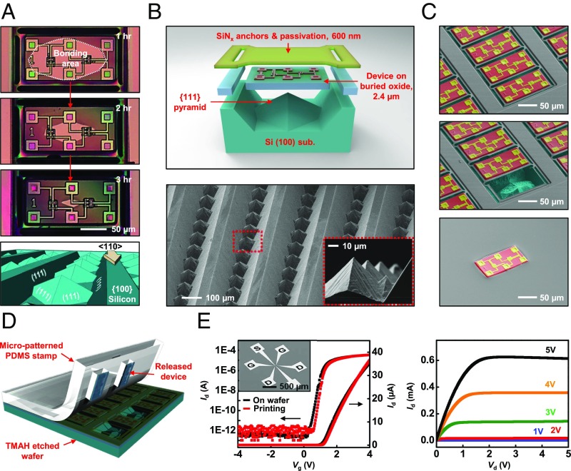
To facilitate release, the orientation of the devices is such that their edges are parallel to the wafer flat (i.e., Si <110>). Here, trench openings created by ICP-RIE along the Si <110> direction allow rapid removal [100-fold faster than Si (111)] of exposed silicon in the Si (110) and Si (100) planes, thereby laterally etching the wafer to undercut the devices. The micrographs in Fig. 2 show a representative device at various stages of undercut with TMAH. The thin geometries (≈3 μm, including the nitride passivation, active device structures, and BOX layer) and the properties of the constituent materials provide sufficient levels of optical transparency to allow direct visualization of regions that remain connected to the underlying silicon wafer (Fig. 2A). As a result, monitoring the progression of the undercut can be performed easily by visible microscope inspection. Careful control, combined with optimized procedures for transfer printing, can lead to cumulative yields of greater than 99%. Schematic illustrations and SEM images of the undercut profiles appear in Fig. 2B. The results are consistent with etching that proceeds in the Si <110> direction, bounded by (111) planes. By consequence, an undercut process that begins at the RIE trenches leaves {111} silicon pyramids positioned at the centers of the device blocks (39).
Fig. 2.
Aspects of release of thin, transient CMOS devices based on anisotropic etching of the Si (100) handle wafer. (A, Top) Optical micrographs collected at 1 h, 2 h, and 3 h after undercut etching to release a representative device (n-channel MOSFET). (A, Bottom) Schematic illustration of the anisotropic etching profile associated with the Si (100) substrate. (B, Top) Schematic exploded view illustration of the structural configuration of a unit cell in an array of devices after complete release. The etched areas are bounded by Si (111) planes, with freely suspended devices tethered by SiNx anchors across the trenches. (B, Bottom) SEM images of etched structures in the Si (100) handle wafer after removal of the released devices. (C) SEM images of an array of devices (colorized using a scheme similar to the scheme in Fig. 1 for ease of viewing), shown in sequence, after undercut etching (Top), after removal of a single device from the handle wafer (Middle), and after transfer printing of this device onto a target substrate (Bottom). (D) Schematic illustration of the process for transfer printing with a PDMS stamp. (E, Left) Linear and log-scale transfer characteristics of an n-channel MOSFET before (black) and after (red) transfer. (E, Right) Output characteristics of the same transistor. Id, drain current; Vg, gate voltage.
Fig. 2C shows SEM images of representative devices in sequence from suspension above the handle wafer to removal and delivery onto a foreign substrate by transfer printing. The BOX serves as an integrated encapsulation layer on the backsides of the devices. The top coating of PECVD SiNx provides not only a passivation layer that isolates the devices from the etching baths but also a strain-compensating layer that reduces bowing of the devices after their release. The transfer printing process uses stamps of poly(dimethylsiloxane) (PDMS) with relief features defined to manipulate one device at a time or large collections of them simultaneously. A schematic representation of this process appears in Fig. 2D. The transfer and output characteristics of typical n-channel metal-oxide-semiconductor field-effect transistors (MOSFETs) processed in this manner are consistent with expected performance [on/off ratio of ≈108, subthreshold slope of ≈100 mV⋅decade−1, on-resistance of ≈18 kΩ at gate voltage (Vg) = 5 V] as shown in Fig. 2E.
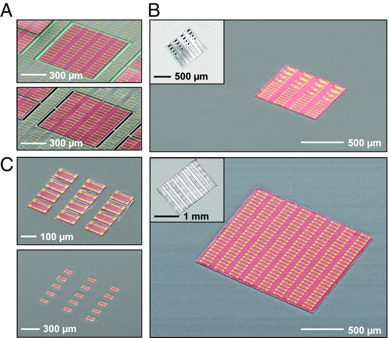
This transfer scheme is compatible with a wide range of sizes and shapes of the device blocks, their distributions across the source wafer, and numbers of them that are manipulated in each cycle of the process. By comparison with traditional pick/place tools, transfer printing is effective with far smaller and thinner devices, and at much higher throughputs. A repetitive sequence of transfer operations can distribute devices over areas on a target substrate that are much larger than those areas defined by the source wafers (40). Certain applications require large numbers of small devices in arrays, as shown in Fig. 3B; others demand only single chips with relatively large lateral dimensions. Fig. 3 shows an example of the latter, in which the devices have dimensions of 0.8 × 1 mm2 and 1.5 × 2 mm2 (Fig. 3C).
Fig. 3.
Released and transfer printed arrays of thin, foundry-based transient electronic devices of various sizes at different area coverages and spatial distributions. (A) SEM images of a 4 × 16 array of diodes before (Top) and after (Bottom) undercut releasing. (B) SEM images of dense (Top, with pitch of 80 μm and 10 μm) and sparse (Bottom, with pitch of 250 μm and 100 μm) collections of device blocks on thin sheets of PLGA, illustrating the scalability of area expansion. (C) SEM images of devices with dimensions of ∼0.8 × 1 mm2 (Top) and ∼1.5 × 2 mm2 (Bottom) printed onto PLGA. (Insets) Optical micrographs. These images are colorized for ease of viewing (cyan, silicon handle wafer; gold, device array; red, released region of foundry-based chips).
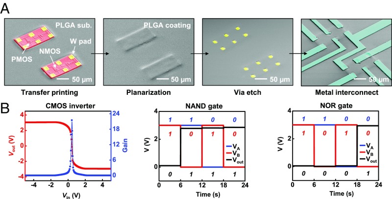
Transferred devices can be interconnected by patterned thin layers of W. The bioresorbable copolymer poly(lactic-coglycolic acid) (PLGA) serves as a transient substrate and planarization layer in the examples in Fig. 4A, where a pair of n-channel and p-channel MOSFETs [channel width (W) = 6 μm, channel length (Lch) = 1.8 μm for n-channel MOSFETs, Lch = 1 μm for p-channel MOSFETs] yields CMOS logic gates. The posttransfer process begins with application of a planarizing coating of PLGA, using an anisole-based solution to prevent printed devices from washing away during the spin-coating process. This solvent is attractive because its high volatility minimizes dissolution of the PLGA substrate. The resulting coating conforms to the step edges at the perimeters of the devices (≈3 μm in height) to facilitate formation of interconnects over these features. Plasma etching through a photolithographically patterned hard mask of Mg (100 nm) creates openings through the PLGA at the positions of the contact pads on the device blocks. The positively sloped sidewalls that result from this etching process facilitate continuous metal interconnects patterned by photolithography and etching. Fig. 4B shows output voltage characteristics for a CMOS inverter (Left), a negative-AND (NAND) (Middle), and a negative-OR (NOR) (Right) circuit obtained in this manner. For the inverter, the voltage transfer characteristics exhibit gains of up to ≈21 at supply bias levels of ±3 V, with input low voltage (VIL) of 0.05 V and input high voltage (VIH) of 0.85 V, capable of a large noise margin for high noise immunity. For the NAND and NOR gates, the output voltages below 0.1 V and over 2.8 V are considered as a logic low (0) state and a logic high (1) state, respectively, with the input voltages, VA and VB, switching between 0 V (for the 0 state) and 3 V (for the 1 state) to drive particular functions for the logic gates.
Fig. 4.
Microscale assembly/integration of foundry-based transient CMOS devices on PLGA substrates. (A) Sequence of SEM images to illustrate the process for forming interconnects to a representative pair of n-channel and p-channel MOSFETs. The colorized regions correspond to original contact pads (yellow), individual device units (red), and interconnect leads (blue). (B) Output voltage characteristics of a CMOS inverter (Left), a NAND gate (Center), and a NOR gate (Right). The supply voltage is 3 V. Vin, input voltage.
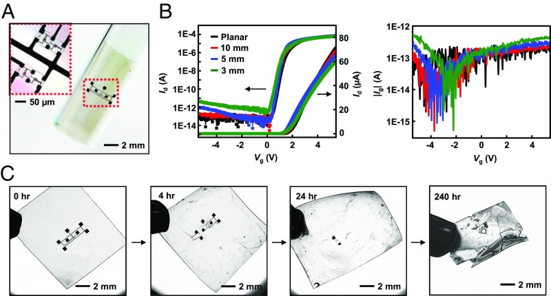
The resulting systems are mechanically flexible by virtue of their small thicknesses and the bendability of the PLGA substrates, as exemplified in Fig. 5A. Bending into cylinders with various diameters reveals invariant operating properties for radii of curvature as small as a few millimeters (Fig. 5B). Specifically, electrical measurements on n-channel MOSFETs at such curvatures indicate on/off ratios of >107, with mobilities from 610 to 680 cm2⋅V−1. The observed systematic variations likely arise from bending-induced strains in the channel and associated changes in charge carrier mobilities. With the simple approximation that the bending strain is where x is parallel to the channel length in the Si <110> direction, R is the bending radius, and t is the thickness of the flexible electronic systems, the expected mobility enhancement, is ∼1.5% (for R = 5 mm), ∼4.2% (for R = 2.5 mm), and ∼7.7% (for R = 1.5 mm) under the induced uniaxial tensile strain and at an effective field of 0.4 MV⋅cm−1 (41, 42). The data indicate device mobilities of 624 cm2⋅V−1 (for planar), 618 cm2⋅V−1 (for R = 5 mm), 657 cm2⋅V−1 (for R = 2.5 mm), and 677 cm2⋅V−1 (for R = 1.5 mm) that are qualitatively consistent with this mechanism and with data on related devices reported elsewhere (43, 44).
Fig. 5.
Foundry-based transient electronic systems on a PLGA substrate. (A) Optical micrographs of transient logic gates (similar to the transient logic gates shown in Fig. 3) on a thin film of PLGA wrapped onto a glass cylinder. (Inset) Magnified view of the interconnected MOSFETs. (B) Current-voltage characteristics of typical n-channel MOSFETs mounted on cylinders with different diameters. Ig, gate leakage current. (C) Optical micrographs at various stages of dissolution and disintegration of transient electronics that integrate foundry-based microelectronics on the thin PLGA sheet. This accelerated dissolution test is performed in an aqueous buffer solution (pH 7.4) at 70 °C.
The entire systems dissolve in water, beginning with the PLGA. A sequence of images captured during dissolution in PBS (pH 7.4) at 70 °C appears in Fig. 5C. In this example, hydrolytic degradation of the PLGA leads to swelling and buckling processes that cause fracture and disintegration of the W traces within 24 h. The PLGA loses its mechanical strength via random chemical scission of the ester backbone and resulting changes in morphology, pH, and crystalline properties, resulting in the degradation or failure of the interconnected system at this stage (45, 46). By comparison, the device blocks dissolve much more slowly, in a manner determined by the constituent materials and their corresponding structures as described in detail subsequently. Timescales for complete dissolution of the PLGA sheets (≈20 µm) are ∼15–20 d, as determined by the chemical composition and molecular weight.
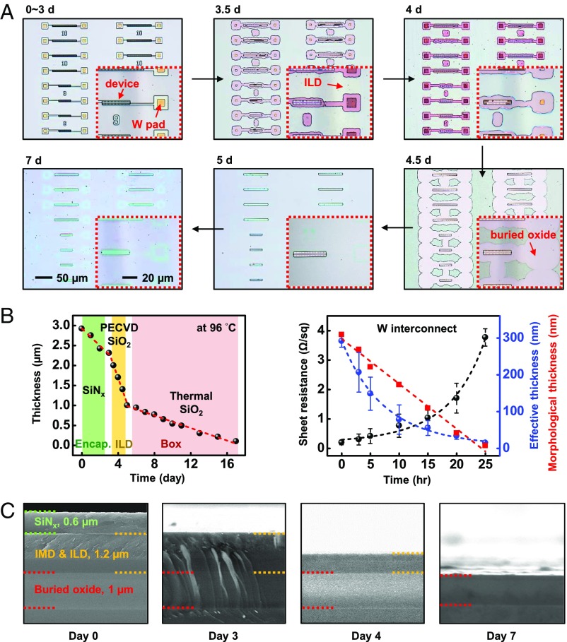
Accelerated tests (immersion in PBS at 96 °C) provide information on the kinetics of dissolution of the devices themselves. Fig. 6A presents a series of optical images collected during dissolution of an array of devices similar in materials and layout to the components in Fig. 1. In this example, apparent physical changes in device morphology imply material decomposition as a result of soaking. The changes initiate at structural edges, followed in other regions by successive downward etching, on a layer-by-layer basis. Extrinsic material properties, such as porosity, pitting, or other nonuniformities, can influence the process. Additional details obtained by measuring thicknesses as a function of time further establish the kinetics of hydrolysis of W, PECVD SiNx, PECVD SiO2, and thermal SiO2. The data appear in Fig. 6B, where the morphological thicknesses correspond to physical changes measured directly by profilometry and the effective thicknesses correspond to approximate changes derived from measured sheet resistances, Rs, according to (with constant resistivity and an initial thickness of 300 nm). Corresponding stages of dissolution in physical transience are shown in Fig. 6C. Hydrolysis consumes SiNx in a uniform fashion at a rate of ∼0.2 μm⋅d−1 according to Si3N4 + 6H2O → 3SiO2 + 4NH3, followed by the dissolution of the PECVD SiO2 interlayer [SiO2 + 2H2O → Si(OH)4] at a rate of ∼0.7 μm⋅d−1; in the meantime, W interconnects (2W + 2H2O + 3O2 → 2H2WO4) and Si layers dissolve [Si + 4H2O → Si(OH)4 + 2H2] on timescales of 24 h. After the layered structure mostly disappears, the underlying BOX (thermally grown SiO2) dissolves over the following 10 d, thereby establishing the overall timescale for transience. These results are consistent with previous reports of dissolution kinetics for nonfoundry silicon-based transient electronics (21, 47–49).
Fig. 6.
Evolution of device structures and material layers in transient electronic devices during dissolution. (A) Optical images of arrays of devices during accelerated dissolution upon immersion in an aqueous buffer solution (pH 7.4) at 96 °C. The device structures include SiNx encapsulation (≈600 nm), W interconnects (≈300 nm), PECVD SiO2 interlayers (≈1.2 μm), and Si active layers (≈250 nm), with an underlying layer of SiO2 (≈1 μm; BOX). (B) Time evolution of device thickness associated with different constituent materials during the dissolution test. The estimated dissolution rates are ∼0.2 μm⋅d−1 for PECVD SiNx, ∼0.7 μm⋅d−1 for PECVD SiO2, <0.1 μm⋅d−1 for thermal SiO2, and ∼0.3 μm⋅d−1 for W. (C) Cross-sectional SEM images collected at several stages of device dissolution. The decreases in device thickness account for the dissolution rate and data in B. The SEM images were taken at 13,000× magnification.
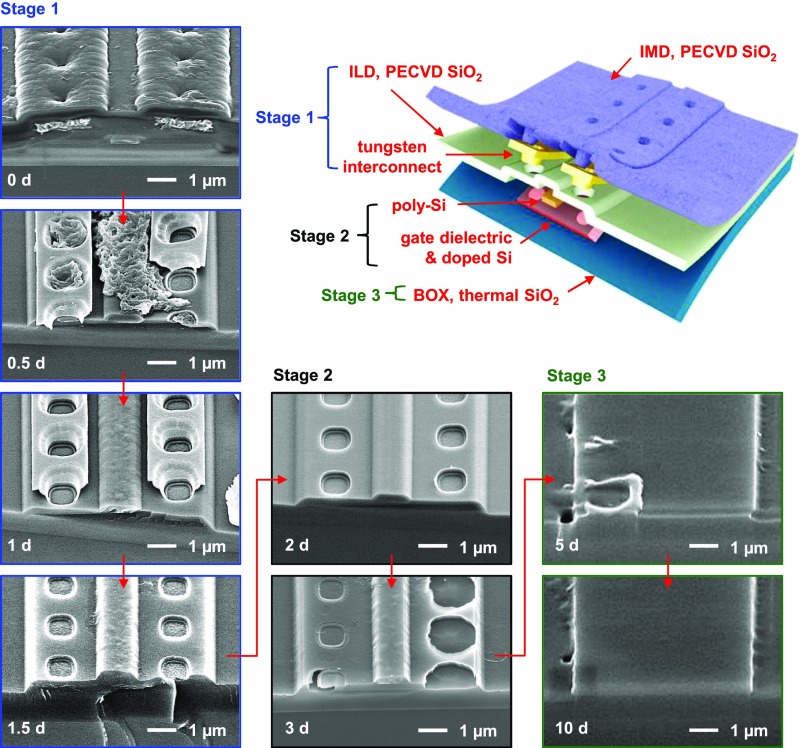
Corresponding changes in microstructure during dissolution of a single device can be studied via cross-sectional SEM, as shown in Fig. 7. The schematic illustration provides information on the structure and material constituents: PECVD SiO2 for IMD (≈650 nm) and ILD (≈750 nm) layers, W (≈300 nm) for metal interconnects, Ti/TiN (≈100 nm) for the adhesion promoter, thermal SiO2 (≈1 μm) BOX, and device Si (≈250 nm), including the polycrystalline silicon gate (≈80 nm), doped silicon, and SiO2 gate dielectric (≈25 nm). Each component, except the Ti/TiN adhesive layer, dissolves in a manner determined by the corresponding hydrolysis rates of the materials, the presence and type of morphological defects (e.g., pores/pinholes/microcracks), and the characteristics of the surrounding solution (pH, temperature, agitation/convection). The first stage corresponds to disintegration of the IMD and ILD layers and the W interconnects, beginning with the exposed W at the contact pads. Reactive dissolution that undercuts the embedded W lines exfoliates the layered structure due to permeation of the PBS, followed by delamination of the Ti/TiN layer. This type of disintegration occurs mostly due to delamination, peeling, and formation of flakes. Although Ti undergoes oxidation (Ti + 2H2O → TiO2 + 2H2), further chemical reactions are typically terminated by the oxide product (50). Hence, the Ti/TiN layer tends to peel off after disintegration of the supporting ILD layer during this dissolution stage. The second stage involves dissolution of the active Si, starting along structural relief in a fashion that depends on the presence of residual ILD material (etching barriers or natural microvoids from local defects). Finally, the thermal SiO2 slowly dissolves during the last stage, typically in a spatially uniform fashion across the entire area. As shown in the SEM images, PBS soaking tests leave patterns on the BOX layer with the lateral dimensions of devices. Immersion for ∼2 wk leads to complete dissolution under these conditions; at 5 d, everything except the BOX is eliminated. Clearly, a decrease in the BOX thickness will reduce the overall dissolution time (e.g., foundry-based transient electronics with 100-nm-thick BOX layer are projected to dissolve within a week under these conditions).
Fig. 7.
Disintegration of layered microstructures in a transient electronic device during dissolution. A schematic illustration and a time sequence of SEM images of disintegration of foundry-based transient microelectronic devices are shown. The device structure and test conditions for the dissolution test are the same as in Fig. 6.
Conclusion
The materials, fabrication strategies, and integration schemes reported here enable the use of foundry-compatible, full-wafer processing capabilities in transient electronics. Microscale assembly of state-of-art CMOS devices onto soft materials avoids constraints in materials choices that would otherwise follow from foundry-standard manufacturing temperatures, processing solvents, and other conditions that are incompatible with bioresorbable polymers. Anisotropic etching as a release strategy and selective transfer printing as a means for device manipulation provide versatility in forming functional systems with wide-ranging application possibilities. The outcomes could qualitatively extend conventional foundry-based manufacturing capacity and affiliated supporting infrastructure in circuit and device design to nearly all envisioned applications in transient electronics. These findings enable the translation of modern chip technologies into environmentally friendly, biodegradable systems.
Materials and Methods
Fabrication of Foundry-Based Transient Logic Gates.
Fully formed microelectronics fabricated on 6-inch SOI (100) wafers with active layers of Si (≈250 nm), gate oxide (≈25 nm), ILD (≈750 nm) and IMD (≈650 nm) layers, Ti/TiN (≈100 nm), and W interconnects (≈300 nm) as the source of transient active devices. The Ti/TiN layer at the via plugs, which comprises less than 1% of the overall area of a typical device and less than 0.05% of its overall mass, is the only component that is not water-soluble. Photolithography and ICP-RIE (STS Mesc Multiplex) with SF6 yielded isolated device blocks. This ICP-RIE step formed trenches to the underlying Si (100) handle wafer through the IMD, ILD, and BOX layers. A 600-nm-thick, low-stress SiNx layer deposited by PECVD (STS Mesc Multiplex tool; mixed frequency RF power of 20 W) served as the material for the anchors and etching barriers. An additional ICP-RIE step defined the former so as to tether the device blocks to their lithographically defined locations and to prevent them from washing away during the undercut etching process. This etching involved complete immersion in a static solution of 8.3% TMAH (at 85 °C) or 18% KOH (at 70 °C). Devices released in this way exist in a freely suspended configuration, suitable for transfer printing from the source wafer onto a target substrate. To facilitate this transfer process, a thin sheet of PLGA (Sigma–Aldrich) annealed at temperatures near the glass transition of the PLGA (65 °C; molecular weight of 50,000–75,000) served as the receiving substrate. A spin-cast layer of PLGA (85:15; 2 μm thick) planarized the resulting platform, following transfer. A thin film of Mg (100 nm) deposited by sputtering and patterned by photolithography and etching provided a hard mask for etching through the PLGA by RIE to expose the contact pads of the underlying device blocks. Removal of the Mg, followed by patterning of the sputtered layer of W (300 nm) by photolithography and etching, completed the fabrication.
Dissolution Testing.
A transparent PDMS enclosure bonded to the surface of a processed wafer confined a volume of PBS (pH 7.4; Sigma–Aldrich) for dissolution testing in a manner that allowed for in situ observation with an optical microscope. A programmable hotplate controlled the temperature. The PBS solutions were replaced every other day during the course of dissolution. For ex situ characterization (Hitachi S4800 SEM system or FEI DB235 focus ion beam system), the samples were removed from the enclosure and gently rinsed with deionized water. Electrical characterization was performed with a semiconductor parameter analyzer (4155C; Agilent) and a probe station in a dark box. Measurements of the W interconnection involved a cylindrical four-point probe setup (Jandel) to determine the sheet resistance (and, with appropriate calibration, the thickness) and a profilometer (Dektak) and/or atomic force microscope (MFP-3D; Asylum Research) to determine the thicknesses.
Acknowledgments
We thank the Micro and Nanotechnology Laboratory and the Micro-Nano-Mechanical Systems Laboratory at the University of Illinois at Urbana–Champaign for device fabrication and material characterization. We thank Dr. Dan Harburg for informative discussions. This work was supported by the Center for Bio-Integrated Electronics at Northwestern University. J.-K.C. received support from Ministry of Science and Technology, Taiwan (Project 105-2917-I-564-038).
Footnotes
The authors declare no conflict of interest.
References
- 1.Venema L. Silicon electronics and beyond. Nature. 2011;479:309. doi: 10.1038/479309a. [DOI] [PubMed] [Google Scholar]
- 2.Bagley B. 2016 28th International Symposium on Power Semiconductor Devices and ICs (ISPSD) IEEE; Prague, Czech Republic: 2016. Semiconductor financing: Recent trends; pp. 1–4. [Google Scholar]
- 3.Zhu Y, Xiong J. Proceedings of the IEEE/ACM International Conference on Computer-Aided Design. IEEE Press; Piscataway, NJ: 2015. Modern big data analytics for old-fashioned semiconductor industry applications; pp. 776–780. [Google Scholar]
- 4.World Semiconductor Trade Statistics 2017 WSTS Semiconductor Market Forecast Spring 2017. WSTS Forecasts the Semiconductor Market’s Largest Growth Year in More Than Five Years. Available at: https://www.wsts.org/PRESS/Recent-News-Release. Accessed March 28, 2017.
- 5.Lorenzen JA. Green consumption and social change: Debates over responsibility, private action, and access. Sociol Compass. 2014;8:1063–1081. [Google Scholar]
- 6.Tanskanen P. Management and recycling of electronic waste. Acta Mater. 2013;61:1001–1011. [Google Scholar]
- 7.Fang S, et al. An integrated system for regional environmental monitoring and management based on internet of things. IEEE Trans Industr Inform. 2014;10:1596–1605. [Google Scholar]
- 8.Da Xu L, He W, Li S. Internet of things in industries: A survey. IEEE Trans Industr Inform. 2014;10:2233–2243. [Google Scholar]
- 9.Zhou Y, et al. Efficient recyclable organic solar cells on cellulose nanocrystal substrates with a conducting polymer top electrode deposited by film-transfer lamination. Org Electron. 2014;15:661–666. [Google Scholar]
- 10.Kang SK, et al. Bioresorbable silicon electronic sensors for the brain. Nature. 2016;530:71–76. doi: 10.1038/nature16492. [DOI] [PubMed] [Google Scholar]
- 11.Jung YH, et al. High-performance green flexible electronics based on biodegradable cellulose nanofibril paper. Nat Commun. 2015;6:7170. doi: 10.1038/ncomms8170. [DOI] [PMC free article] [PubMed] [Google Scholar]
- 12.Huang X, et al. Biodegradable materials for multilayer transient printed circuit boards. Adv Mater. 2014;26:7371–7377. doi: 10.1002/adma.201403164. [DOI] [PubMed] [Google Scholar]
- 13.Kim BH, et al. Dry transient electronic systems by use of materials that sublime. Adv Funct Mater. 2017;27:1606008. [Google Scholar]
- 14.Bettinger CJ, Bao Z. Organic thin-film transistors fabricated on resorbable biomaterial substrates. Adv Mater. 2010;22:651–655. doi: 10.1002/adma.200902322. [DOI] [PMC free article] [PubMed] [Google Scholar]
- 15.Irimia-Vladu M. “Green” electronics: Biodegradable and biocompatible materials and devices for sustainable future. Chem Soc Rev. 2014;43:588–610. doi: 10.1039/c3cs60235d. [DOI] [PubMed] [Google Scholar]
- 16.Muskovich M, Bettinger CJ. Biomaterials-based electronics: Polymers and interfaces for biology and medicine. Adv Healthc Mater. 2012;1:248–266. doi: 10.1002/adhm.201200071. [DOI] [PMC free article] [PubMed] [Google Scholar]
- 17.Hwang SW, et al. Materials for programmed, functional transformation in transient electronic systems. Adv Mater. 2015;27:47–52. doi: 10.1002/adma.201403051. [DOI] [PubMed] [Google Scholar]
- 18.Hwang SW, et al. A physically transient form of silicon electronics. Science. 2012;337:1640–1644. doi: 10.1126/science.1226325. [DOI] [PMC free article] [PubMed] [Google Scholar]
- 19.Hwang SW, et al. High-performance biodegradable/transient electronics on biodegradable polymers. Adv Mater. 2014;26:3905–3911. doi: 10.1002/adma.201306050. [DOI] [PubMed] [Google Scholar]
- 20.Kang SK, et al. Biodegradable thin metal foils and spin‐on glass materials for transient electronics. Adv Funct Mater. 2015;25:1789–1797. [Google Scholar]
- 21.Kang SK, et al. Dissolution behaviors and applications of silicon oxides and nitrides in transient electronics. Adv Funct Mater. 2014;24:4427–4434. [Google Scholar]
- 22.Yin L, et al. Dissolvable metals for transient electronics. Adv Funct Mater. 2014;24:645–658. [Google Scholar]
- 23.Kang SK, et al. Dissolution chemistry and biocompatibility of silicon- and germanium-based semiconductors for transient electronics. ACS Appl Mater Interfaces. 2015;7:9297–9305. doi: 10.1021/acsami.5b02526. [DOI] [PubMed] [Google Scholar]
- 24.Yu KJ, et al. Bioresorbable silicon electronics for transient spatiotemporal mapping of electrical activity from the cerebral cortex. Nat Mater. 2016;15:782–791. doi: 10.1038/nmat4624. [DOI] [PMC free article] [PubMed] [Google Scholar]
- 25.Fu K, et al. Transient rechargeable batteries triggered by cascade reactions. Nano Lett. 2015;15:4664–4671. doi: 10.1021/acs.nanolett.5b01451. [DOI] [PubMed] [Google Scholar]
- 26.Hwang SW, et al. Biodegradable elastomers and silicon nanomembranes/nanoribbons for stretchable, transient electronics, and biosensors. Nano Lett. 2015;15:2801–2808. doi: 10.1021/nl503997m. [DOI] [PubMed] [Google Scholar]
- 27.Hwang SW, et al. Materials for bioresorbable radio frequency electronics. Adv Mater. 2013;25:3526–3531. doi: 10.1002/adma.201300920. [DOI] [PubMed] [Google Scholar]
- 28.Edupuganti V, Solanki R. Fabrication, characterization, and modeling of a biodegradable battery for transient electronics. J Power Sources. 2016;336:447–454. [Google Scholar]
- 29.Fu KK, et al. Transient electronics: Materials and devices. Chem Mater. 2016;28:3527–3539. [Google Scholar]
- 30.Chen Y, et al. Characterizing physically transient antennas. IEEE Trans Antennas Propag. 2015;63:2421–2429. [Google Scholar]
- 31.Patrick E, Orazem ME, Sanchez JC, Nishida T. Corrosion of tungsten microelectrodes used in neural recording applications. J Neurosci Meth. 2011;198:158–171. doi: 10.1016/j.jneumeth.2011.03.012. [DOI] [PMC free article] [PubMed] [Google Scholar]
- 32.Chen Q, Thouas GA. Metallic implant biomaterials. Mater Sci Eng R-Rep. 2015;87:1–57. [Google Scholar]
- 33.Kim DH, et al. Complementary logic gates and ring oscillators on plastic substrates by use of printed ribbons of single-crystalline silicon. IEEE Electron Device Lett. 2008;29:73–76. [Google Scholar]
- 34.Baca AJ, et al. Printable single‐crystal silicon micro/nanoscale ribbons, platelets and bars generated from bulk wafers. Adv Funct Mater. 2007;17:3051–3062. [Google Scholar]
- 35.Sun L, et al. 12-GHz thin-film transistors on transferrable silicon nanomembranes for high-performance flexible electronics. Small. 2010;6:2553–2557. doi: 10.1002/smll.201000522. [DOI] [PubMed] [Google Scholar]
- 36.Yin L, et al. Materials and fabrication sequences for water soluble silicon integrated circuits at the 90 nm node. Appl Phys Lett. 2015;106:014105. [Google Scholar]
- 37.Riches S, Johnston C. 2015 IEEE International Symposium on Circuits and Systems. IEEE; Lisbon, Portugal: 2015. Electronics design, assembly and reliability for high temperature applications; pp. 1158–1161. [Google Scholar]
- 38.Paun MA, Udrea F. Investigation into the capabilities of Hall cells integrated in a non-fully depleted SOI CMOS technological process. Sens Actuators A Phys. 2016;242:43–49. [Google Scholar]
- 39.Landsberger LM, Naseh S, Kahrizi M, Paranjape M. On hillocks generated during anisotropic etching of Si in TMAH. J Microelectromech Syst. 1996;5:106–116. [Google Scholar]
- 40.Carlson A, Bowen AM, Huang Y, Nuzzo RG, Rogers JA. Transfer printing techniques for materials assembly and micro/nanodevice fabrication. Adv Mater. 2012;24:5284–5318. doi: 10.1002/adma.201201386. [DOI] [PubMed] [Google Scholar]
- 41.Sun Y, Thompson SE, Nishida T. Physics of strain effects in semiconductors and metal-oxide-semiconductor field-effect transistors. J Appl Phys. 2007;101:104503. [Google Scholar]
- 42.Gamiz F, Cartujo-Cassinello P, Roldán JB, Jiménez-Molinos F. Electron transport in strained Si inversion layers grown on SiGe-on-insulator substrates. J Appl Phys. 2002;92:288–295. [Google Scholar]
- 43.Kim HS, et al. Self-assembled nanodielectrics and silicon nanomembranes for low voltage, flexible transistors, and logic gates on plastic substrates. Appl Phys Lett. 2009;95:183504. [Google Scholar]
- 44.Zhao W, He J, Belford RE, Wernersson LE, Seabaugh A. Partially depleted SOI MOSFETs under uniaxial tensile strain. IEEE Trans Electron Dev. 2004;51:317–323. [Google Scholar]
- 45.Göpferich A. Mechanisms of polymer degradation and erosion. Biomaterials. 1996;17:103–114. doi: 10.1016/0142-9612(96)85755-3. [DOI] [PubMed] [Google Scholar]
- 46.Athanasiou KA, Niederauer GG, Agrawal CM. Sterilization, toxicity, biocompatibility and clinical applications of polylactic acid/polyglycolic acid copolymers. Biomaterials. 1996;17:93–102. doi: 10.1016/0142-9612(96)85754-1. [DOI] [PubMed] [Google Scholar]
- 47.Hwang SW, et al. Materials and fabrication processes for transient and bioresorbable high‐performance electronics. Adv Funct Mater. 2013;23:4087–4093. [Google Scholar]
- 48.Fang H, et al. Ultrathin, transferred layers of thermally grown silicon dioxide as biofluid barriers for biointegrated flexible electronic systems. Proc Natl Acad Sci USA. 2016;113:11682–11687. doi: 10.1073/pnas.1605269113. [DOI] [PMC free article] [PubMed] [Google Scholar]
- 49.Hwang SW, et al. Dissolution chemistry and biocompatibility of single-crystalline silicon nanomembranes and associated materials for transient electronics. ACS Nano. 2014;8:5843–5851. doi: 10.1021/nn500847g. [DOI] [PubMed] [Google Scholar]
- 50.Oshida Y. Bioscience and Bioengineering of Titanium Materials. Elsevier; London: 2010. [Google Scholar]


