Abstract
Current developments in positron emission tomography (PET) focus on improving timing performance for scanners with time-of-flight (TOF) capability, and incorporating depth-of-interaction (DOI) information. Recent studies have shown that incorporating DOI correction in TOF detectors can improve timing resolution, and that DOI also becomes more important in long axial field-of-view scanners. We have previously reported the development of DOI-encoding detectors using phosphor-coated scintillation crystals; here we study the timing properties of those crystals to assess the feasibility of providing some level of DOI information without significantly degrading the timing performance. We used Monte Carlo simulations to provide a detailed understanding of light transport in phosphor-coated crystals which cannot be fully characterized experimentally. Our simulations used a custom reflectance model based on 3D crystal surface measurements. Lutetium oxyorthosilicate (LSO) crystals were simulated with a phosphor coating in contact with the scintillator surfaces and an external diffuse reflector (teflon). Light output, energy resolution, and pulse shape showed excellent agreement with experimental data obtained on 3 × 3 × 10 mm3 crystals coupled to a photomultiplier tube (PMT). Scintillator intrinsic timing resolution was simulated with head-on and side-on configurations, confirming the trends observed experimentally. These results indicate that the model may be used to predict timing properties in phosphor-coated crystals and guide the coating for optimal DOI resolution/timing performance trade-off for a given crystal geometry. Simulation data suggested that a time stamp generated from early photoelectrons minimizes degradation of the timing resolution, thus making this method potentially more useful for TOF-DOI detectors than our initial experiments suggested. Finally, this approach could easily be extended to the study of timing properties in other scintillation crystals, with a range of treatments and materials attached to the surface.
Keywords: Positron emission tomography (PET), scintillation detectors, light transport, timing properties, Monte Carlo simulation, depth-of-interaction (DOI), phosphor-coated scintillation crystals
1 Introduction
Current developments in positron emission tomography (PET) largely focus on improving timing performance for scanners with time-of-flight (TOF) capability, and incorporating depth-of-interaction (DOI) information. Combining good timing resolution, typically less than 600 ps to significantly improve image quality (Karp et al., 2008), and DOI resolution is challenging, and often one parameter has to be prioritized over the other. In clinical PET scanners, the distance between the detectors and the patient is usually greater than that in small-animal scanners, which results in a smaller parallax error and makes TOF capability more critical for improving image quality. However, PET detectors have now achieved timing resolutions that are good enough to be affected by depth-dependent timing dispersion, and several studies have shown value in including DOI information in detectors using long crystals (>20 mm) in order to further improve timing resolution (Moses and Derenzo, 1999; Shibuya et al., 2008; Spanoudaki and Levin, 2011; Wiener et al., 2013). DOI correction also becomes more important in long axial field-of-view clinical scanners where axial DOI blurring may significantly degrade spatial resolution (Poon et al., 2012).
Among the various methods proposed to encode DOI, notable approaches include dual-ended readout of the scintillator (Yang et al., 2008), and the phoswich detector composed of several layers of scintillators with different decay times (Jung et al., 2007; Eriksson et al., 2009). Other designs include multi-layer scintillator arrays with offset crystals (Ito et al., 2010), arrangements with light sharing between crystal layers (Nishikido et al., 2010), and monolithic detectors (Maas et al., 2009; Miyaoka et al., 2010). In an effort to provide continuous DOI information while using readout from a single end of the detector, we have proposed applying a phosphor coating on scintillator crystals to modify the decay time of the detected pulses in a depth-dependent manner (Du et al., 2009). A fraction of the scintillation light is absorbed by the phosphor and is re-emitted with a delay due to the intrinsic decay time of the phosphor. DOI information may then be extracted from the pulse shape (Roncali et al., 2012).
Initial studies showed that a DOI resolution of 8 mm full-width at half-maximum (FWHM) could be obtained in 1.5 × 1.5 × 20 mm3 lutetium oxyorthosilicate (LSO) crystals coated with a Y3(Al)5O12:Ce (YAG) phosphor mixture. We also showed that this method was better suited to crystals with larger cross-sections (typically greater than or equal to 2 mm × 2 mm). This approach is simple, cost-effective and represents a promising solution when only limited DOI resolution is needed. This original optimization focused on achieving good DOI resolution without regard to timing, using unpolished crystals. Unpolished crystals showed a larger decay time variation between the two ends of the crystal compared with polished crystals, most likely because a larger amount of scintillation light escapes the crystal and interacts with the phosphor. However they generally show poor timing performance and are not suitable for TOF PET. More recently, our interest in developing a long axial field-of-view scanner with TOF and DOI capability (Cherry, 2006; Poon et al., 2012) led us to reconsider the application of phosphor coating to polished crystals, in order to assess the feasibility of providing limited DOI information without significantly degrading the timing performance.
The optimization of phosphor-coated crystals requires studying a vast parameter space, which if done solely experimentally is costly (a large number of crystals is needed), time-consuming (coating the crystals is currently a manual process), and still does not provide a complete description of the coating performance because some parameters, such as the conversion efficiency of the coating, cannot be directly measured. In addition to studying key parameters such as the conversion efficiency, we are seeking to understand the contribution of the coating to crystal timing performance, which depends on the scintillation emission process and the light transit time in the crystal. The separation of those two components is not possible experimentally, as the temporal distribution of the light collected at the exit faces of the crystal is governed by both effects. Furthermore, the typical output of photodetectors is a photoelectron rate, not individual photoelectron time stamps. Collecting those would require a photon counting system that typically work with levels of light lower than that of a scintillation pulse, and thus may not allow all photoelectron time stamps to be recorded for a given pulse. By contrast, simulation allows access to all the information regarding the arrival times and generation of individual photons and photoelectrons, without the confounding contribution of the photodetector itself.
Significant effort has been devoted to understanding the different contributions to timing resolution using Monte Carlo simulation, including the light transport in the scintillator, the photodetector response and the timing pick-off method (Choong, 2009; Spanoudaki and Levin, 2011; Yang et al., 2013). We have proposed a novel model of surface reflectance based 3D measurements of the crystal surfaces, that allows for the accurate computation of light transport in crystals with a range of surface treatments (Roncali and Cherry, 2013). Here we apply this model to the study of light transport in phosphor-coated crystals with polished surfaces, including for the first time predictions of timing-related properties. We have developed a model of the phosphor coating in contact with the scintillator surfaces. The model includes the phosphor decay time, and excitation and emission spectra, to allow the effect of different coating shapes, thicknesses, and materials to be studied. The goal of this work was two-fold. First, 3 × 3 × 10 mm3 phosphor-coated LSO crystals were simulated and the resulting energy resolution, light output, and pulse shape were compared to experimental results to determine whether our model of optical emission, transport and detection could predict trends observed in the experimental data. Second, we applied this model to study the effect of the coating, the DOI and the timing pick-off on the timing properties for different coating schemes. As the goal of this work was to predict the scintillation light pulses produced by the coated crystal, the timing properties of the photodetector and associated electronics were not included in the simulations.
2 Materials & Methods
2.1 Crystals and Coating
Four 3 × 3 × 10 mm3 LSO crystals, with all their surfaces polished, were used. After measuring the light output, pulse shape at different depths and timing resolution using the protocol described in section 2.2.1, the crystals were subsequently coated with YAG phosphor. The coating was a mixture by weight of 45% YAG powder (Comtech International Inc., Korea) and 55 % optical cement (NOA 88, Norland Products, NJ). For this phosphor material, we measured a decay time of 58 ns, an absorption peak at 430 nm, and an emission peak at 540 nm. The coating was manually applied on the first crystal face to be coated, using a shim to achieve a coating thickness of 250 μm. The coating was cured for ∼120 s with a UV lamp (Super Spot MK II, Lesco UV, CA). After curing, the process was repeated on the other crystal faces. The crystals were then baked at 90°C for 12 hours to increase the adhesion of the coating to the crystal surfaces (Roncali et al., 2014). Two crystals had half the length of their four sides plus the face opposite to the PMT face (which will be referred to as the top face in the rest of the paper) coated with phosphor (Figure 1a), one crystal had only the top face coated (Figure 1b). To assess the simulation model with a different type of coating, an additional crystal had half the length of its four sides and the top face coated with black ink (Figure 1c). This coating absorbs the scintillation light regardless of its wavelength, without re-emission so that no light can re-enter the crystal after absorption.
Figure 1.
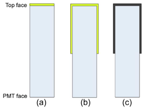
a) The phosphor coating was applied on the top face only. b) The top face and half the length of the 4 sides were coated with phosphor. c) Same as b) with a black ink instead of phosphor.
2.2 Light collection and timing measurements
2.2.1 DOI measurements
Crystals were wrapped in teflon tape and coupled to a single-channel photomultiplier tube (Hamamatsu R6231) using optical grease (BC-630, Bicron). The detector, composed of the crystal of interest coupled to the photomultiplier tube (PMT), was positioned in coincidence with a collimating detector composed of an uncoated 3 × 3 × 10 mm3 LSO crystal wrapped in teflon tape and coupled to a R9800 PMT and irradiated at three different depths (1 mm, 5 mm, and 9 mm from the PMT face) by a 0.5 mm 22Na point source of activity 3.7 MBq (Roncali et al., 2012). The zero depth was set at the PMT face and the estimated width of the collimating beam at the crystal was 1.5 mm. The coincidence events were used to trigger the acquisition of ∼1000 individual pulses at each depth by a fast oscilloscope (Lecroy WavePro 7100) with a sampling interval of 0.1 nsec for each pulse. Light outputs were normalized relative to the photopeak values acquired with the uncoated crystals at 1mm.
2.2.2 Timing measurements
Timing measurements were performed using two Hamamatsu R9800 PMTs with standard bialkali photocathodes. Two different detector orientations were used: a head on and side on orientation, for cumulative depth and depth-dependent measurements, respectively. For the side-on geometry the beam width was estimated to be 3 mm. The PMT signals were first amplified using a high bandwidth amplifier (TI 4302, Texas Instruments, Dallas TX) and then split with one branch used for timing and the other for energy. Time pick-off was performed using constant fraction discrimination (CFD) with an Ortec 935 (Ametek, Oak Ridge TN). The CFD output was then sent to a time-to-amplitude converter (Tennelec, Oak Ridge TN) and the output was digitized by a data acquisition board (United Electric Industries, (Judenhofer et al., 2005)). For the coincidence timing measurements, the reference detector was composed of an uncoated 3 × 3 × 10 mm3 LSO crystal wrapped in teflon tape and coupled to a R9800 PMT. For each timing measurement, 200,000 events were recorded. The intrinsic timing resolution of a single reference detector was measured to be 201 ps and was subtracted in quadrature from the timing resolution results, in order to report the expected detector timing resolution.
2.3 Simulation of light transport in the crystal
2.3.1 Light transport and surface reflectance model
We have developed a light transport model based on 3D measurements of the scintillator surface. 90 μm × 90 μm areas of crystal surfaces were scanned using an Asylum MFP-3D atomic force microscope (Asylum Research, Santa Barbara CA) to compute the surface reflectance properties. The angular distributions of reflectance, and reflected rays, were calculated for incidence angles varying from 0 to 90° and stored in look-up tables (LUTs). The LUTs were integrated in a light transport model. In previous work, the surface reflectance model was described in detail together with the custom Monte Carlo code developed to model gamma interactions occurring at different depths in a scintillator and generate light pulses (Roncali and Cherry, 2013). This approach allows for the accurate modelling of polished and rough surfaces in contact with various media and was previously applied to crystals in contact with air and wrapped in teflon tape. Here, we extend the use of our Monte Carlo simulation code to crystals coated with a phosphor or black paint.
For each gamma interaction, the energy was randomly selected following a distribution derived from the measured energy spectrum shown in Figure 2a, and visible photons were emitted isotropically with a light yield of 25 photons/keV (Moszynski et al., 1997). For each photon, appropriate wavelength and emission time were assigned based on measured scintillator properties and literature values. The decay time and emission spectrum were measured with time-resolved fluorescence spectroscopy (Fang et al., 2004), while the rise time was taken from the literature (Seifert et al., 2012). Accordingly, the emission times assigned to individual photons followed a bi-exponential distribution with a 72 ps rise time and 46 ns decay time, while the wavelength of the generated photons was selected by randomly sampling the emission spectrum. The bulk LSO material was modelled with an index of refraction of 1.82, an absorption length of 300 mm and a scattering length of 256 mm (Rothfuss et al., 2004). Individual photons were tracked in the volume of the scintillator until they exited the crystal. When a photon reached the edges of the scintillator, the LUTs were used to determine whether it was reflected or transmitted. For surfaces coated with the phosphor (Figure 2b), the index of refraction of the coating was assumed to be close to that of the optical cement (1.6). When a photon was converted by the phosphor, a new time and wavelength were assigned. The times assigned to individual photons followed an exponential distribution with a 58 ns decay (measured with time-resolved fluorescence spectroscopy). All surfaces except the crystal face in contact with the PMT were covered with an external diffuse reflector with a reflection coefficient of 0.97 to model a 40 μm-thick teflon tape, with an air gap between the reflector and the surface of the crystal or the coating. The Teflon reflector was modelled as Lambertian reflector. Once a photon exited the crystal at the scintillator/photodetector interface, the probability of generating a photoelectron was based on the quantum efficiency of a standard bialkali photocathode (Hamamatsu Photonics K.K., 2006). The crystal face was assumed to be coupled to the PMT entrance window with a thin layer of optical grease (index of refraction 1.5). Photon emission times, photoelectron production times, and wavelengths of detected photons were recorded and used to generate simulated light pulses and spectra.
Figure 2.
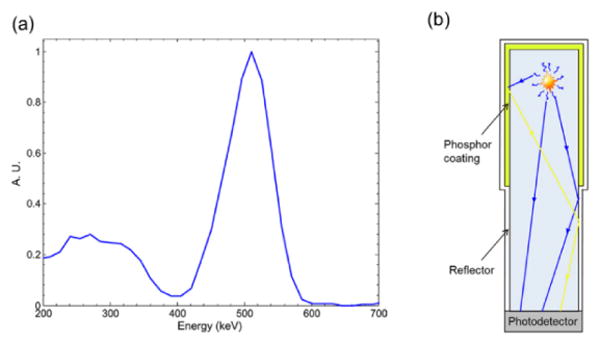
a) Energy distribution used to generate gamma interactions in the crystal. b) Scintillation photons may be reflected in the crystal (in blue) or converted by the phosphor (in yellow).
2.3.2 Modelling of the phosphor coating
When a photon entered the phosphor coating, its fate was determined by its probability of (i) being converted (absorbed and re-emitted) and returning into the crystal, (ii) re-entering the crystal without having been converted, or (iii) escaping the crystal through the reflector. Those probabilities varied with the wavelength of the photon and were calculated using a simplified model of the phosphor layer, consisting of a 3 × 5 × 0.25 mm3 block of YAG phosphor (for a 3 × 3 × 10 mm3 crystal coated on half of its sides with a thickness of 0.25 mm). The YAG material was characterized by its absorption coefficient μa, scattering coefficient μs, anisotropy factor g, and quantum yield. The values for those parameters were chosen from the literature for a concentration of ∼0.75 g/cm3 to match the experimental coating (Liu et al., 2010). g was set at 0.86 and the values of μa and μs were set at 4 and 70 mm-1 at 455 nm. μs was considered constant over the visible spectrum whereas values of μa at other wavelengths were calculated from the YAG excitation spectrum. The quantum yield for the YAG powder was 0.97 (value from the manufacturer). All sides of the YAG block except the 3 mm × 5 mm face in contact with the crystal were modelled as wrapped in teflon tape.
To compute the probability of (i) and (ii) at different wavelengths between 400 nm and 650 nm, 1000 incident photons were aimed at the 3 mm × 5 mm face at each wavelength (every 10 nm). (i) was defined as the fraction of incident photons converted and reflected back to the incident medium (index of refraction 1.82) with a different wavelength, whereas (ii) corresponded to the fraction of incident photons reflected back with their incident wavelength. Individual photons were tracked in the phosphor using a diffusion model (Prahl et al., 1989). The probability of a photon escaping the phosphor was derived from the sum of (i) and (ii) and all probabilities at different wavelengths were stored in LUTs. The use of LUTs to determine the fate of scintillation photons when interacting with the phosphor greatly reduces the computation time, as it avoids tracking each photon in real time.
The black paint coating was modelled similarly to the YAG phosphor coating, except that the absorption coefficient was set to a high value of 1000 mm-1 and the conversion efficiency was set to 0 (when absorbed, the photons do not generate any light).
2.4 Simulations for comparison to experimental results
For each crystal, 200 light pulses were generated in 1.5 mm bins every 2 mm, starting at 1 mm from the PMT face. Four types of crystals were simulated: uncoated crystals, crystals with half the length of the four sides + top face phosphor-coated, crystals with only the top face phosphor-coated and crystals with black paint on the top face and half the length of the sides. For each type of crystal, simulations were repeated four times. Photon emission times and wavelengths of detected photons were histogrammed to generate simulated light pulses and spectra. The energy of individual pulses was computed as the integrated number of photoelectrons. At each depth, the energies were histogrammed and the photopeak positions were used to characterize the light output variation with depth. All light output values were normalized by the photopeak position at 1 mm DOI, the irradiation depth closest to the PMT face.
2.5 Study of timing properties
Time zero was defined when the gamma rays entered in the crystal, i.e. at the top face (10 mm from the PMT face). Before interacting with the scintillator at a given depth, the gamma rays travelled at the speed of light (3×10⁸ m/s2). The transit time of the scintillation light after emission was obtained from the total distance travelled by photons ultimately detected by the PMT, using the speed of light in LSO. The photoelectron production time was computed as the sum of the gamma travel time, the scintillation and phosphor photon emission time, and the transit time of that photon to the PMT photocathode.
2.5.1 Effect of DOI: side-on configuration
All photoelectron production times were stored and sorted in ascending order, to be used to compute the scintillator intrinsic timing resolution for various photoelectron thresholds. Photoelectron production times for all gamma interactions were histogrammed to build a distribution. The DOI effect on timing properties was first studied by studying how the photoelectron production time distribution peak position shifts with depth. Secondly, another side-on configuration similar to the experimental setup (section 2.2.2) was simulated and the scintillator intrinsic timing resolution was computed at three DOI (1 mm, 5 mm, and 9 mm). The reference detector was modelled as aligned with the source (see section 2.5.2) whereas the second one was perpendicular and irradiated in 1.5 mm bins. The contribution from the reference detector was subtracted in quadrature from the scintillator intrinsic timing resolution.
2.5.2 Scintillator intrinsic timing resolution for head-on configuration
To compute the scintillator intrinsic timing resolution, two identical detectors placed in coincidence at equal distance from a source were simulated using the events generated at different DOIs (section 2.4). For each gamma pair, first DOIs in the crystal were randomly selected. The two DOIs were sampled independently from an exponential distribution which is maximal at the top face of the crystal (i.e. 10 mm away from the PMT face) and characterized by the gamma attenuation coefficient in LSO (0.87 cm-1, (Melcher and Schweitzer, 1992). Then, two events generated at depths closest to the two chosen DOIs were selected and the photoelectron production times corresponding to the desired photoelectron threshold were identified. The difference of those two times, defined as the coincidence time, was stored and two new events were selected until 10,000 coincidence times were obtained. This number was chosen to ensure that the risk of drawing the same pair of events more than once was very small (less than 2% with ∼800 pulses in each crystal). The coincidence times were histogrammed to build a coincidence timing spectrum and extract the coincidence timing resolution using a Gaussian fit. The two virtual detectors were assumed to have similar performance and the scintillator intrinsic timing resolution was computed as the coincidence timing resolution / √2.
3 Results
3.1 Comparison of simulations and experimental results
3.1.1 Light output
For the four different coating schemes, the relative photopeak positions (Figure 3) showed good agreement between simulated and experimental data. The simulations showed excellent reproducibility, with less than 1% relative variation, which made the error bars too small to be shown in Figure 3. The uncoated and top face simulated light output differed by less than 2% from the experimental results. The black-painted crystals were only measured at 1 mm and 9 mm and also showed good agreement experiments (∼7% difference). The larger difference observed for the half-sides phosphor-coated crystals (17% overestimation) is most likely due to the difficultly in exactly knowing the optical properties of the phosphor material used in the experiments. For each configuration, the variation of the simulated photopeak position with DOI followed the same trend as the experimental values and revealed a decrease of the photopeak position with increasing distance from the photodetector for the half side-coated crystals. This is important, as it shows that the model accurately describes the light loss along the sides of the crystal, which is critical in modelling the light transport and ultimate light detection.
Figure 3.
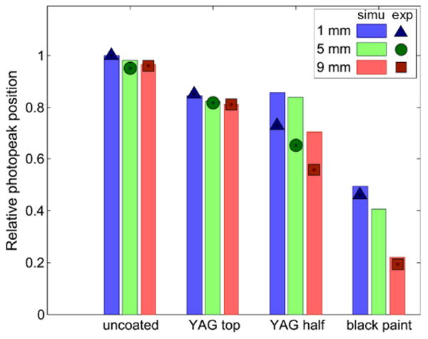
Bars show the simulated photopeak positions normalized by the uncoated crystal value at 1 mm DOI, for three different depths. Points show that the experimental photopeak positions, normalized by the uncoated crystal photopeak at 1 mm, follow the same trend as the simulations.
For uncoated crystals, no depth-dependency of the energy resolution was observed either in simulations or measured data, and values were in close agreement (Table 1). As expected, coating half the length of the crystal sides degraded the energy resolution in a depth-dependent manner. For each configuration, the standard deviation of the simulated energy resolution values was within 0.1%, which confirmed the reproducibility of the simulations.
Table 1.
Measured and simulated energy resolution at different DOI.
| Configuration | DOI | |||
|---|---|---|---|---|
|
| ||||
| 1 mm | 5 mm | 9 mm | ||
| Uncoated crystal | (simulated) | 13.2% | 13.2% | 13.2% |
| (measured) | 12.8% | 12.8% | 12.8% | |
|
| ||||
| Top face coated | (simulated) | 15.0% | 15.0% | 15.0% |
| (measured) | 14.4% | 14.4% | 14.4% | |
|
| ||||
| 1/2 sides YAG | (simulated) | 16.0% | 16.0% | 18.1% |
| (measured) | 15.2% | 16.1% | 17.2% | |
3.1.2 Pulse shape
For both simulated and experimental characterization of the crystals, individual pulses recorded at each DOI were averaged (200 simulated pulses per depth and ∼1000 pulses recorded at each depth) and fitted with a single exponential to compute the corresponding decay times (Figure 4). Although the decay time of averaged pulses is typically not used to compute the DOI of individual pulses (Roncali et al., 2012), it predicts the DOI resolution and allows for a rapid comparison between configurations. Figure 4 shows that simulated and measured pulses agreed well in their decay time and the change in decay time with DOI.
Figure 4.
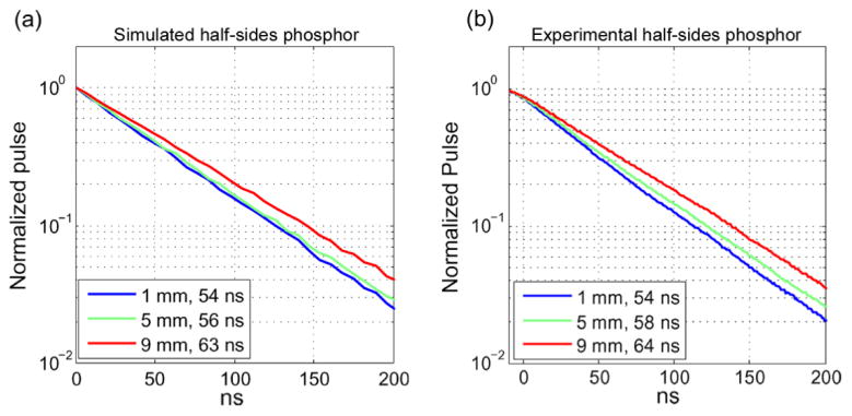
a) Simulated pulse shapes (200 pulses averaged at each DOI). b) Measured pulse shape (∼1000 pulses averaged at each DOI).
Decay times of individual pulses were also computed. The variation of the mean decay time with DOI is shown in Figure 5, with error bars representing the standard deviation. The uncoated crystals (in blue) showed no variation of the decay time with DOI, as expected. Similarly, the top face coated crystals (in red) showed no depth-dependency but an overall increase of 4.9 ns (experimental) and 3.1 ns (simulated) in decay time compared to uncoated crystals. The simulated half-sides coated crystals showed an increase of 8.6 ns between the ends of the crystals, which agreed well with the measured data (10.4 ns). The small discrepancy between simulations and experiments is likely due to the parameters modelling the phosphor coating.
Figure 5.
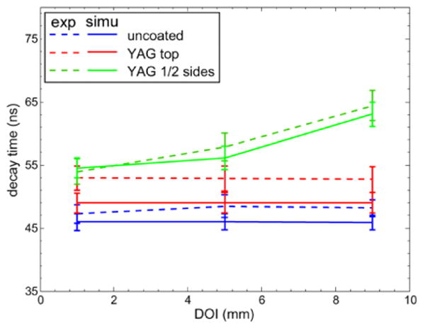
Average decay times for simulated (solid lines) and experimental (dashed) data.
Based on the good agreement between simulated and experimental data for light output, energy resolution and pulse shape, the simulation tools now can be used to explore questions regarding DOI and timing in phosphor-coated crystals that cannot be easily addressed experimentally.
3.2 Effect of the coating on the light collection: spectral analysis
In the simulation, each individual photoelectron corresponds to a detected scintillation photon whose emission wavelength was recorded. Figure 6a shows that at all depths, emission peaks of uncoated crystals were located at 420 nm, which corresponds to the LSO emission peak. In contrast, when applying a phosphor coating on half the crystal sides (Figure 6b), the spectrum exhibited a second peak at 540 nm. The amplitude of this peak increased for interactions further from the photodetector, reflecting the increasing conversion by the phosphor (emission peak at 540 nm). However even the spectrum at 1 mm DOI showed a second peak, indicating that some conversion occurred at that depth as well. An ideal coating would provide no conversion at 1 mm and total conversion at 9 mm. In contrast, coating only the top face extended the emission spectrum in the yellow but did not create any significant DOI dependency (spectra not shown here), which explains the absence of decay time variation with depth. This illustrates the importance of the simulation to gain a better understanding of the coating behaviour.
Figure 6.
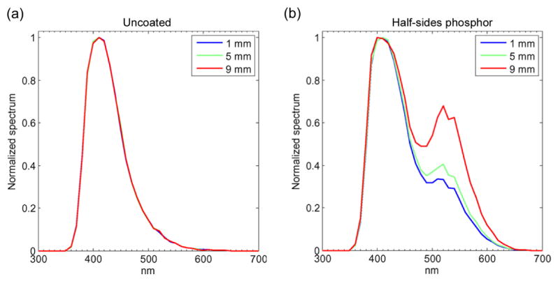
Normalized simulated average emission spectrum at each DOI. a) Uncoated crystal shows a peak at 420 nm and no depth dependence. b) Half-sides coated crystal shows a shift of the emission spectrum with DOI.
3.3 Effect of the coating on timing properties: side-on configuration
3.3.1 Transit time in the crystal
For each photoelectron produced, the transit time of the corresponding scintillation photon in the crystal was recorded. The gamma photon time-of-flight before interaction with the crystal was added to the light transit times, which were then histogrammed at each irradiation depth (Figure 7). Here, emission time was not included. For both configurations, the photoelectron production time distribution shifted with increasing distance from the photodetector as the photons had to travel a longer distance before reaching the PMT face. The shift was partially compensated by the gamma time-of-flight, because gamma rays interacting at 1 mm had a longer path in the crystal when entering the crystal by the face opposite to the PMT.
Figure 7.
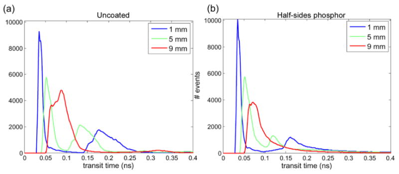
Simulated transit time in the crystal. a) Uncoated crystals show two peaks that become more pronounced for interactions close to the PMT face. b) Half-sides phosphor coating decreases the amplitude of the second peaks.
For the uncoated crystal (Figure 7a), the histograms were characterized by a first peak, with a rising edge corresponding to the minimum time required to reach the photodetector and a second peak, with a rising edge corresponding to the transit time of photons that were emitted away from the PMT and reflected from the top face directly back to the photodetector. Photons have a finite probability of traversing the crystal length multiple times prior to detection, giving rise to the low amplitude peaks at later times (Figure 7a). The separation of the two peaks decreased as the source moved further from the photodetector, consistent with other studies (Yeom et al., 2013). When applying a coating, the peak locations for all DOI positions did not show significant variation as compared to the uncoated crystals. However, the half-sides coating greatly reduced the second peak amplitude while the amplitude of the first peak did not change (Figure 7b). This can be explained by the fact that the coating on the top face and sides reduces the index mismatch (1.82/1 for coated surfaces vs. 1.82/1.6 for coated crystals) and thus decreases the number of secondary reflections.
The distribution of the transit times gives insight on how the coating modifies the light transport in the crystal and potentially affects the scintillator intrinsic timing resolution. In order to fully characterize their contribution, the transit times must be considered together with the emission times.
3.3.2 First photoelectron production time distribution
Because of the variation of scintillation light transit time combined with the statistical process of the scintillation emission, the production time of the first photoelectron (and subsequent photoelectrons) produced from a given interaction depth in the crystal will vary. Figure 8 shows the predicted distribution of the first photoelectron production time for 200 events at each depth, for both the uncoated crystals and the half-sides phosphor-coated crystals. When the crystal was irradiated 1 mm from the PMT face, the coating had a minimal effect on the distribution (blue curves in Figure 8). When irradiating the crystal at 5 and 9 mm, the YAG phosphor coating extended the tail of the distribution to the right and decreased the peak amplitude (relative to the uncoated crystals) while the peak location was almost unchanged (green and red curves in Figure 8). Coating the top face only did not change the distributions, whereas coating half the sides of the crystal with black paint further extended the tails to the right (data not shown here). These results suggest that the observed tail on the coated crystals is not primarily due to the delay of converted photons by the absorption/reemission process, but is caused by the increased light loss through the crystal surfaces in the coated crystals which reduces the probability of early emitted photons reaching the PMT and creating photoelectrons.
Figure 8.
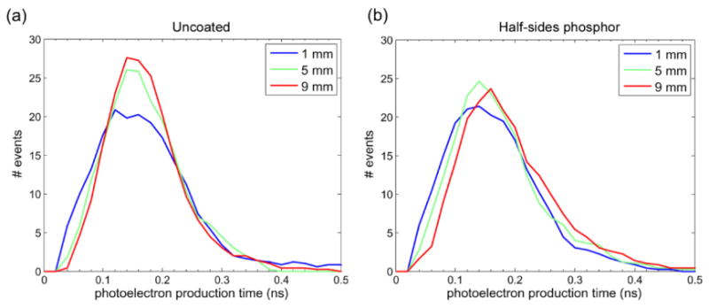
Simulation results: Distribution of the first photoelectron production times. a) For the uncoated crystals the distributions FWHM decreased with DOI (from 0.182 ns to 0.132 ns). b) For the half sides phosphor, the FWHM decrease with DOI was less important (from 0.176 ns to 0.153 ns).
The effect of DOI also depended on the coating. In Figure 8a, the distributions became narrower (as measured by the FWHM) with increasing distance from the photodetector (larger DOI values). As shown in Figure 8b, this effect was smaller with the phosphor coated crystals (decrease of 23 ps FWHM instead of 54 ps between 1 mm and 9 mm). The width of the distribution is indicative of the scintillator intrinsic timing resolution, as dispersion in the photoelectron production time will translate into a dispersion of the triggering time for coincidence events. Examining these distributions of first photoelectron production times, we would expect some improvement of the uncoated crystal intrinsic timing resolution for depths far from the PMT, and less dependence in the timing resolution of the half-sides coated crystal with DOI.
3.3.3 Scintillator intrinsic timing resolution in side-on configuration
Figure 9 summarizes the scintillator intrinsic timing resolution simulated in a side-on configuration at three different DOI, 1, 5, and 9 mm. For each of the four simulation runs for each configuration, the scintillator intrinsic timing resolution was computed 10 times (error bars represent the standard deviation across the 40 samples) without any energy window. For different thresholds varying from 1 to 10 photoelectrons, scintillator intrinsic timing resolution values were computed by fitting each coincidence spectrum with a Gaussian (R2 values 0.94-0.99). Figure 9a shows that the scintillator intrinsic timing resolution for uncoated crystals was depth-dependent. At all DOI, the scintillator intrinsic timing resolution for uncoated crystals degraded when triggering on a higher number of photoelectrons, however it degraded more rapidly for the 1 mm irradiation depth. Between 1 mm and 9 mm for a threshold at 10 photoelectrons, there was a 27 ps decrease in timing resolution, whereas for the very first photoelectron it was 20 ps. Considering the error bars, the observed improvement of the intrinsic timing resolution with increasing distance from the photodetector is not inconsistent with predictions from the distribution of the first photoelectron production times (Figure 8a). A slight improvement of the scintillator intrinsic timing resolution with increasing distance from the photodetector is also in line with experimental data when measuring the detector timing resolution with a CFD (Table 2).
Figure 9.
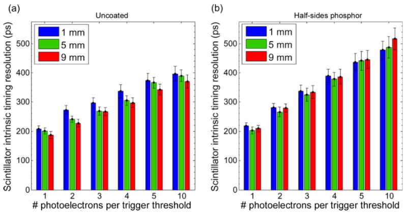
Simulated scintillator intrinsic timing resolution, side-on configuration.
Table 2.
Experimentally measured detector timing resolution at two DOIs (side-on configuration) using CFD-based timing.
| Configuration | DOI | |
|---|---|---|
|
| ||
| 1 mm | 9 mm | |
| Uncoated crystal | 204 ps | 197 ps |
| 1/2 sides YAG coated | 237 ps | 295 ps |
The phosphor-coated crystals also showed a DOI-dependency (Figure 9b) at higher photoelectron triggering thresholds. Trigger at or above the 10th photoelectron, the scintillator intrinsic timing resolution degraded with increasing distance from the photodetector, opposite to the effect seen in the uncoated crystals. A possible explanation to this result is that the coating generates light loss along the sides of the crystal, which degrades the detection statistics and thus the timing resolution.
The variation of scintillator intrinsic timing resolution with DOI was greater when triggering on a higher number of photoelectrons. When triggering on the first photoelectron, the scintillator intrinsic timing resolution at 1 mm and 9 mm were similar, whereas when triggering on the 10th photoelectron there was a degradation of 39 ps between 1 mm and 9 mm.
At all photoelectron thresholds, the half-sides coated crystals showed equal or higher timing resolution values than the uncoated crystals.
Detector timing measurements showed a degradation of 58 ps between 1 mm and 9 mm DOI for the coated crystals and a slight improvement of 7 ps for the uncoated crystals (Table 2). Although the values are not directly comparable because the simulations did not include the photodetector contribution and were done with a leading-edge timing pick-off whereas the experiments were done with a CFD, it is important that the simulations and experiments followed a similar trend. This suggests that the light transport in the crystal is being appropriately modelled.
3.4 Effect of the timing pick-off in head-on configuration
The scintillator intrinsic timing resolution was also computed by simulating two identical detectors in coincidence in a head-on configuration for both uncoated crystals and half-sides coated crystals (Figure 10). In order to provide a comparison of the crystals in the exact same conditions, no energy window was applied; all events were used. As expected, the scintillator intrinsic timing resolution was best when triggering on the first photoelectron for both crystals (191 ps and 220 ps for uncoated and coated respectively) and values were close to side-on simulations. The difference between the uncoated crystals and half-sides coated crystals became larger with higher photoelectron threshold. This result is important, as it suggests that by triggering on the earliest photoelectrons it may be possible to preserve the timing resolution while encoding the DOI information using a phosphor coating. Finally, the detector timing resolution measured for both crystal types using a head-on experimental setup and a CFD-based time-pick-off showed an increase of 70 ps (Table 3), which is consistent with the trends displayed by the simulations.
Figure 10. Simulated scintillator intrinsic timing resolution, head-on configuration.
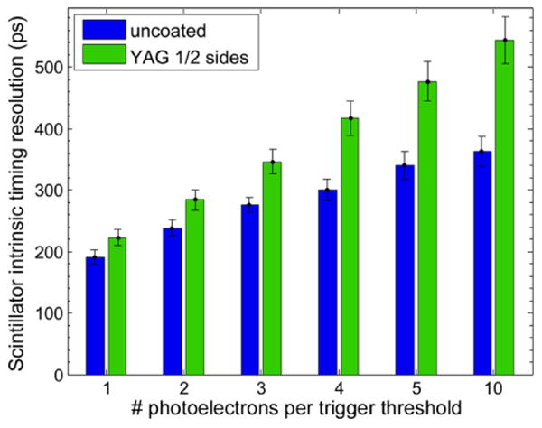
Table 3. Measured detector timing resolution (head-on configuration).
| Configuration | |
|---|---|
| Uncoated crystal | 287 ps |
| 1/2 sides YAG coated | 384 ps |
4 Discussion
In our previous work, we reported the development of a reflection model to accurately simulate light transport in scintillators (Roncali and Cherry, 2013). Here, we have extended this work to phosphor-coated crystals to encode DOI information. A model of the phosphor coating was integrated in our Monte Carlo simulation tool and applied to four different coating schemes (including uncoated crystals). Simulations of 3 × 3 × 10 mm3 polished LSO crystals showed excellent agreement with experiments in terms of light output, energy resolution, and pulse shape and demonstrated that the model could be used to predict timing properties and to study the effect of coating scintillation crystals. In particular, the DOI effect on scintillator intrinsic timing resolution showed a similar trend to experimental data for uncoated crystals, in which the resolution seemed to be best further from the PMT face, and for phosphor-coated crystals where the opposite effect was observed. The simulation studies presented here do not include detailed modelling of the photodetector and focused on investigating how the coating affected the light transport in the scintillator itself rather than providing a direct comparison of experimental and simulated timing resolution. While the photodetector plays a key role in defining the ultimate detector timing resolution, here only the crystal modelling was of interest to understand how the phosphor coating impacted the time at which early photoelectrons were generated. The contribution of the photodetector and associated electronics to the timing performance, especially in the context of readout of phosphor-coated crystals using silicon photomultipliers, may be investigated in future work.
Monte Carlo simulations performed in this work allowed for the study of unique aspects of phosphor-coated crystals and advanced the understanding of the different processes involved in the light transport and ultimate detection. The light emission spectrum can be used to assess the fraction of converted light that reaches the photodetector but is not detected because of the lower PMT quantum efficiency at the phosphor emission wavelength. The model also allows for detailed studies of the effect of DOI, which will be critical when applying the model to longer crystals where the DOI dependency is more important. Finally, the predicted scintillator intrinsic timing resolution suggests that it may be possible to optimize the timing pick-off by triggering on the first photoelectron, allowing the use of phosphor coating to encode DOI without significantly degrading the timing performance. This may lead to a viable time-of-flight PET detector that also encodes some DOI information.
Small discrepancies between simulations and measurements were observed with the half-sides coated crystals and are likely due to the limited accuracy of the phosphor coating parameters. The main challenge in applying this model to the optimization of a coating lies in the lack of information on the phosphor material, which led us to use values estimated from the literature. In addition, the coating composed of phosphor powder mixed with optical cement is heterogeneous, therefore important characteristics such as absorption and scattering coefficients are extremely difficult to measure without a dedicated and costly optical setup. The overall ability of the model to predict the light transport and temporal properties in the crystal, even when some assumptions were made, is very promising. Our model now allows the simulation of scintillation crystals with a range of surface treatments and materials attached to it, including temporal properties, which makes it a versatile tool for detector design.
Acknowledgments
This work was funded in part by NIH grant R01 CA170874 and in part by a UC Davis Research Investment in Science and Engineering (RISE) grant.
References
- Cherry SR. The 2006 Henry N. Wagner lecture: Of mice and men (and positrons)—advances in PET imaging technology. J Nucl Med. 2006;47:1735–45. [PubMed] [Google Scholar]
- Choong WS. The timing resolution of scintillation-detector systems: Monte Carlo analysis. Phys Med Biol. 2009;54:6495. doi: 10.1088/0031-9155/54/21/004. [DOI] [PMC free article] [PubMed] [Google Scholar]
- Du H, Yang Y, Glodo J, Wu Y, Shah K, Cherry SR. Continuous depth-of-interaction encoding using phosphor-coated scintillators. Phys Med Biol. 2009;54:1757–71. doi: 10.1088/0031-9155/54/6/023. [DOI] [PMC free article] [PubMed] [Google Scholar]
- Eriksson L, Melcher CL, Eriksson M, Rothfuss H, Grazioso R, Aykac M. Design considerations of phoswich detectors for high resolution positron emission tomography. IEEE Trans Nucl Sci. 2009;56:182–8. [Google Scholar]
- Fang Q, Papaioannou T, Jo JA, Vaitha R, Shastry K, Marcu L. Time-domain laser-induced fluorescence spectroscopy apparatus for clinical diagnostics. REVIEW OF SCIENTIFIC INSTRUMENTS. 2004;75:151–62. doi: 10.1063/1.1634354. [DOI] [PMC free article] [PubMed] [Google Scholar]
- Word Technical Writing: Hamamatsu Photonics K.K., Electron Tube Division, editor. Hamamatsu Photonics K.K. Photomultiplier tubes. Basics and applications. 2006. pp. 30–5. [Google Scholar]
- Ito M, Lee JS, Kwon SI, Lee GS, Hong B, Lee KS, Sim KS, Lee SJ, Rhee JT, Hong SJ. A four-layer DOI detector with a relative offset for use in an animal PET system. IEEE Trans Nucl Sci. 2010;57:976–81. [Google Scholar]
- Judenhofer MS, Pichler BJ, Cherry SR. Evaluation of high performance data acquisition boards for simultaneous sampling of fast signals from PET detectors. Phys Med Biol. 2005;50:29. doi: 10.1088/0031-9155/50/1/003. [DOI] [PubMed] [Google Scholar]
- Jung JH, Choi Y, Chung YH, Devroede O, Krieguer M, Bruyndonckx P, Tavernier S. Optimization of LSO/LuYAP phoswich detector for small animal PET. Nucl Instrum Methods Phys Res A. 2007;571:669–75. [Google Scholar]
- Karp JS, Surti S, Daube-Witherspoon ME, Muehllehner G. Benefit of time-of-flight in PET: Experimental and clinical results. J Nucl Med. 2008;49:462–70. doi: 10.2967/jnumed.107.044834. [DOI] [PMC free article] [PubMed] [Google Scholar]
- Liu ZY, Liu S, Wang K, Luo XB. Measurement and numerical studies of optical properties of YAG:Ce phosphor for white light-emitting diode packaging. Appl Opt. 2010;49:247–57. doi: 10.1364/AO.49.000247. [DOI] [PubMed] [Google Scholar]
- Maas MC, Schaart DR, van der Laan DJJ, Bruyndonckx P, Lemaitre C, Beekman FJ, van Eijk CWE. Monolithic scintillator PET detectors with intrinsic depth-of-interaction correction. Phys Med Biol. 2009;54:1893. doi: 10.1088/0031-9155/54/7/003. [DOI] [PubMed] [Google Scholar]
- Melcher CL, Schweitzer JS. Cerium-doped lutetium oxyorthosilicate - a fast, efficient new scintillator. IEEE Trans Nucl Sci. 1992;39:502–5. [Google Scholar]
- Miyaoka RS, Xiaoli L, Lockhart C, Lewellen TK. Comparison of detector intrinsic spatial resolution characteristics for sensor on the entrance surface and conventional readout designs. IEEE Trans Nucl Sci. 2010;57:990–7. doi: 10.1109/TNS.2010.2046675. [DOI] [PMC free article] [PubMed] [Google Scholar]
- Moses WW, Derenzo SE. Prospects for time-of-flight PET using LSO scintillator. IEEE Trans Nucl Sci. 1999;46:474–8. [Google Scholar]
- Moszynski M, Kapusta M, Mayhugh M, Wolski D, Flyckt SO. Absolute light output of scintillators. IEEE Trans Nucl Sci. 1997;44:1052–61. [Google Scholar]
- Nishikido F, Inadama N, Oda I, Shibuya K, Yoshida E, Yamaya T, Kitamura K, Murayama H. Four-layer depth-of-interaction PET detector for high resolution PET using a multi-pixel S8550 avalanche photodiode. Nucl Instrum Methods Phys Res A. 2010;621:570–5. [Google Scholar]
- Poon JK, Dahlbom ML, Moses WW, Balakrishnan Karthik, Wang W, Cherry SR, Badawi RD. Optimal whole-body PET scanner configurations for different volumes of LSO scintillator: A simulation study. Phys Med Biol. 2012;57:4077–94. doi: 10.1088/0031-9155/57/13/4077. [DOI] [PMC free article] [PubMed] [Google Scholar]
- Prahl SA, Keijzer M, Jacques SL, Welch AJ. A Monte Carlo model of light propagation in tissue. In: M GJ, Sliney DH, editors. Proceedings of Dosimetry of Laser Radiation in Medicine and Biology. 1989. pp. 102–11. [Google Scholar]
- Roncali E, Cherry SR. Simulation of light transport in scintillators based on 3D characterization of crystal surfaces. Phys Med Biol. 2013;58:2185–98. doi: 10.1088/0031-9155/58/7/2185. [DOI] [PMC free article] [PubMed] [Google Scholar]
- Roncali E, Phipps JE, Marcu L, Cherry SR. Pulse shape discrimination and classification methods for continuous depth of interaction encoding PET detectors. Phys Med Biol. 2012;57:6571–85. doi: 10.1088/0031-9155/57/20/6571. [DOI] [PMC free article] [PubMed] [Google Scholar]
- Roncali E, Viswanath V, Cherry SR. Design considerations for DOI-encoding PET detectors using phosphor-coated crystals. IEEE Trans Nucl Sci. 2014;61:1–7. [Google Scholar]
- Rothfuss H, Casey M, Conti M, Doshi N, Eriksson L, Schmand M. Monte Carlo simulation study of LSO crystals. IEEE Trans Nucl Sci. 2004;51:770–4. [Google Scholar]
- Seifert S, Steenbergen JHL, v Dam HT, Schaart DR. Accurate measurement of the rise and decay times of fast scintillators with solid state photon counters. J Instrum. 2012;7:P09004. [Google Scholar]
- Shibuya K, Nishikido F, Tsuda T, Kobayashi T, Lam C, Yamaya T, Yoshida E, Inadama N, Murayama H. Timing resolution improvement using DOI information in a four-layer scintillation detector for TOF-PET. Nucl Instrum Methods Phys Res A. 2008;593:572–7. [Google Scholar]
- Spanoudaki VC, Levin CS. Investigating the temporal resolution limits of scintillation detection from pixellated elements: Comparison between experiment and simulation. Phys Med Biol. 2011;56:735–56. doi: 10.1088/0031-9155/56/3/013. [DOI] [PubMed] [Google Scholar]
- Wiener RI, Surti S, Karp JS. DOI determination by rise time discrimination in single-ended readout for tof PET imaging. IEEE Trans Nucl Sci. 2013;60:1478–86. doi: 10.1109/tns.2013.2243166. [DOI] [PMC free article] [PubMed] [Google Scholar]
- Yang X, Downie E, Farrell T, Peng H. Study of light transport inside scintillation crystals for PET detectors. Phys Med Biol. 2013;58:2143. doi: 10.1088/0031-9155/58/7/2143. [DOI] [PubMed] [Google Scholar]
- Yang Y, Wu Y, Qi J, James SS, Du H, Dokhale PA, Shah KS, Farrell R, Cherry SR. A prototype PET scanner with DOI-encoding detectors. J Nucl Med. 2008;49:1132–40. doi: 10.2967/jnumed.107.049791. [DOI] [PMC free article] [PubMed] [Google Scholar]
- Yeom JY, Vinke R, Levin CS. Optimizing timing performance of silicon photomultiplier-based scintillation detectors. Phys Med Biol. 2013;58:1207. doi: 10.1088/0031-9155/58/4/1207. [DOI] [PMC free article] [PubMed] [Google Scholar]


