

Abstract
Recent advances in optical tweezers have greatly expanded their measurement capabilities. A new generation of hybrid instrument that combines nanomechanical manipulation with fluorescence detection—fluorescence optical tweezers, or “fleezers”—is providing a powerful approach to study complex macromolecular dynamics. Here, we describe a combined high-resolution optical trap/confocal fluorescence microscope that can simultaneously detect sub-nanometer displacements, sub-piconewton forces, and single-molecule fluorescence signals. The primary technical challenge to these hybrid instruments is how to combine both measurement modalities without sacrificing the sensitivity of either one. We present general design principles to overcome this challenge and provide detailed, step-by-step instructions to implement them in the construction and alignment of the instrument. Lastly, we present a set of protocols to perform a simple, proof-of-principle experiment that highlights the instrument capabilities.
Keywords: Optical tweezers, Optical trapping, Single-molecule fluorescence, Förster resonance energy transfer, FRET, Confocal microscopy, Fleezers
1 Introduction
Optical traps—or “optical tweezers”—utilize the momentum of light to exert forces on microscopic objects. By tightly focusing a laser beam, a dielectric object such as a micron-sized polystyrene bead can be trapped stably in three dimensions near the focus of light [1]. Beyond its ability to manipulate microscopic objects, an optical tweezer setup is a sensitive quantitative tool. The trap behaves as a linear, “Hookean” spring near its center, and can be used to measure displacements of a trapped bead and the forces exerted on it with sub-nanometer and sub-piconewton (pN) resolution, respectively. This sensitivity range has made optical tweezers a powerful tool to study biological macromolecules at the single molecule level. Optical traps have been used to stretch nucleic acids and proteins, probing their mechanical properties and how secondary and tertiary structures unravel under force [2, 3]. Stretching individual molecules of DNA or RNA has also become a powerful approach to study protein–nucleic acid interactions [4, 5]. Optical tweezers are particularly amenable to the study of molecular motors, which generate forces on pN scales. They have been instrumental in deciphering the mechanism of a wide range of molecular motors involved in cytoskeletal transport, the central dogma, and beyond (reviewed in refs. [6, 7]). Recent advances in design have improved the resolution of these instruments to where it is now possible to observe directly molecular motion on the scale of a single base pair (bp) of DNA. High-resolution optical tweezers [8, 9] now provide unprecedented access to the stepping dynamics of nucleic acid motors (reviewed in ref. [10]): transcription by RNA polymerase with 1 bp resolution [8, 11], translation codon by codon by the ribosome [12], RNA and DNA unwinding by heli-cases at the bp scale [13, 14], and hierarchical bp-scale stepping in translocases [15].
Despite such advances, optical traps have important limitations. Macromolecular dynamics involve conformational changes that are inherently three-dimensional in nature. Most optical trap measurements are ill-equipped to capture this complexity of motion, projecting all movement onto a single axis, along the direction of applied force [16]. As a result, only a limited view of the underlying dynamics is provided. In addition, optical trap measurements have often been limited to investigating systems involving few components, examined in isolation. Many cellular processes, however, involve highly coordinated, multicomponent assemblies. Optical trap assays can be ill-suited to study larger complexes because they typically measure only a single dynamical observable, which does not reveal internal dynamics or coordination within these complexes. These limitations have motivated the development of new single-molecule techniques that can measure complex macromolecular dynamics.
A new generation of hybrid optical tweezers has allowed simultaneous measurement of multiple observables. Optical torque traps exert and measure force and torque simultaneously [17], and several fluorescence optical tweezers (or fleezers) combining fluorescent imaging capabilities with mechanical manipulation have been developed [18–21]. In this chapter, we describe the design of an instrument that combines high-resolution optical tweezers with single-molecule fluorescence microscopy (Fig. 1) [16]. A unique aspect of this instrument, which contrasts with other optical trap/fluorescence designs, is that neither fluorescence detection nor optical trap sensitivity is sacrificed in combining the techniques. The high-resolution fleezers can simultaneously detect fluorescence signals with single-molecule sensitivity, mechanical displacements with sub-nm resolution, and forces with sub-pN resolution [16].
Fig. 1.

Examples of experiments with combined high-resolution optical trap and fluorescence (not to scale). Left panels: Polystyrene microspheres (grey) are held in optical traps (orange cones), tethered by an engineered DNA molecule (blue) containing a variable central segment flanked by long double-stranded DNA (dsDNA) handles. Fluorophores are excited by a green laser (green cone). Right panels: Time traces showing simultaneous measurement of fluorescence and tether extension. (a) Oligonucleotide hybridization. Short oligonucleotides (blue line) labeled with a fluorophore (green disk) bind and unbind to a complementary ssDNA section in the center of the tethered DNA. The fluorescence and change in tether extension upon hybridization are recorded simultaneously. (b) Single-stranded DNA binding protein wrapping dynamics. A tethered DNA molecule containing a short ssDNA region is labeled with a FRET acceptor at the ss-dsDNA junction (red disk). An E. coli single-stranded DNA binding protein (SSB, cyan) labeled with a FRET donor (green disk) binds to and wraps ssDNA around itself. Simultaneous measurement of FRET efficiency and tether extension enables determination of both the position of SSB along the tether and the amount of ssDNA wrapped. The SSB can transiently wrap and unwrap ssDNA under tension (e.g., t = 20 s), and can diffuse one-dimensionally along the ssDNA by reptation (t = 70 s) (data reproduced from ref. [22] with permission from eLife Sciences Publications). (c) UvrD helicase conformational and unwinding dynamics. A tethered DNA molecule contains a hairpin and short ssDNA protein loading site. E. coli UvrD helicase (cyan, blue, grey, and green) is labeled with FRET donor and acceptor pair to differentiate between two possible conformational states: “Open” and “Closed.” Simultaneous measurement of FRET efficiency and number of DNA base pairs of the hairpin unwound by the helicase enables correlation of the conformation with the activity of the helicase. Changes in UvrD conformational state correspond to switches between unwinding and rezipping of the DNA hairpin (reproduced from ref. [23] with permission from AAAS). The proteins in this figure were prepared with VMD [48] using PDB entries 1EYG, 2IS2, and 3LFU
Figure 1 displays three examples of measurements feasible with this instrument. The confocal microscope can either be used to count dye-labeled molecules or to detect dynamics by single-molecule Förster Resonance Energy Transfer (smFRET), while the traps detect mechanical displacements and forces from the DNA molecule stretched between the two trapped beads. In the first example (Fig. 1a), fluorescence is used to detect a dye-labeled oligonucleotide binding to a complementary DNA sequence tethered between trapped beads, while the trap detects the change in extension upon hybridization, as single-stranded (ss)DNA is converted to double-stranded (ds) DNA [16]. In the second (Fig. 1b), E. coli single-stranded DNA binding protein labeled with a single donor fluorophore wraps ssDNA labeled with an acceptor dye. The combination of trap and smFRET is used to distinguish between protein wrapping/unwrapping ssDNA and its diffusion along ssDNA [22]. Finally (Fig. 1c), internal conformational dynamics of E. coli UvrD helicase labeled with a donor and acceptor dye are detected by smFRET simultaneously with detecting its unwinding of a DNA hairpin by optical trap [23].
Stability and sensitivity are key to this instrument’s performance. We use a dual trap design (Fig. 1), in which both traps are formed from the same laser, as it provides exceptional stability [9]. As a consequence, trapping is done away from the sample chamber surface, and we detect fluorescence using confocal microscopy (as opposed to total internal reflection microscopy often used in surface-based assays). An important technical challenge is that fluorophores photobleach very quickly near an optical trap. This results from the fluorophore absorbing trap infrared photons while in the excited state, leading to a transition into a dark state [24]. Since this mechanism requires absorption of both fluorescence excitation and trap light, one solution is to separate the optical trap and fluorophore by a large distance, preventing simultaneous exposure of the dye to both light sources [19]. However, this approach is not conducive to high-resolution measurement. It necessitates long molecules to tether to the trapped beads, which are compliant and poor transducers of mechanical signals. High resolution requires close proximity between trap and fluorophore, and the solution is to separate the two light sources in time [25]. By interlacing the two light sources at a high rate, i.e., turning them on and off out of phase, it is possible to attain a 20-fold improvement in photobleaching lifetime over exposing the fluorophore simultaneously to fluorescence excitation and trapping light [25].
In this chapter, we describe in detail the design and construction of our hybrid high-resolution optical trap/confocal microscope (for an overview, see Fig. 2). We note that many protocols for building and aligning optical traps have been discussed elsewhere [26–28], and we do not repeat these here. Instead, we focus on the complexities specific to combining single-molecule fluorescence detection with optical traps. We provide a detailed parts list, optical layout, and general design principles to build the instrument. Since interlacing is an essential feature of the instrument, we devote much of the chapter to the materials and protocols for precise timing and synchronization of the light sources and data acquisition. We also provide detailed protocols for aligning the confocal microscope to the optical traps. Lastly, materials and protocols are given for doing a simple, proof-of-principle experiment to measure the binding of a fluorescently labeled oligonucleotide to a complementary single-stranded DNA molecule tethered between trapped beads (Fig. 1a).
Fig. 2.

Protocol summary. (a) Sequence of major steps involved in assembling and aligning the instrument. (b) Materials for the trap + fluorescence assay are prepared in parallel, including two sets of functionalized beads: anti-digoxigenin (ADig) beads and streptavidin (Strep) beads, and stock solutions of glucose oxidase + catalase (GOx) and trolox (TX). (c) Major steps involved in setting up a trap + fluorescence assay
2 Materials
2.1 Optical Trap Setup
There are many considerations in designing and constructing an optical trap, many of which are beyond the scope of this chapter. We refer the reader to the many excellent resources on this topic [26, 28, 29]. The combined optical trap/confocal microscope layout relies on general design principles that maximize stability, spatial and temporal resolution, and control. The instrument is housed in a temperature-regulated, acoustically isolated room, and built on a thick optical table levitated on pneumatic isolators. All optical components that the trap or fluorescence lasers impinge on are mounted to the optical table by 1″-thick pedestals. Wherever possible, high-performance optomechanical components (e.g., kinematic mirror mounts, translation stages) are used and are equipped with locking screws so that they can be fixed after alignment. We also adhere to the general philosophy of “less is more,” i.e., the fewest components should be used to achieve a specific purpose. Our experience is that more components increase the coupling of noise into the instrument. In contrast to many optical trap designs, we also do not integrate the traps into an inverted microscope body. This provides us with complete control over all instrument components and more flexibility in design.
The overall optical layout consists of three separate “modules”: one for the optical trap, one for the fluorescence confocal microscope, and one for the bright-field imaging system (Fig. 3 and 4). We discuss the optical trap module first. General construction and alignment procedures are not discussed in detail, as these can be found elsewhere [26, 27]. Instead, we focus only on those features unique to the instrument and on its essential components: (1) trapping laser, (2) acousto-optic modulator, (3) objective, and (4) detectors.
Fig. 3.

Detailed layout of the instrument (to scale). FC fiber clamp; ISO optical isolator; HW half-wave plate; PBS polarizing beam-splitting cube; BD beam dump; AOM acousto-optic modulator; L lens; M mirror; BS beam-splitter; QPD quadrant photodiode; DM dichroic mirror; FO front objective; BO back objective; F filter; RL relay lens; TL tube lens; ND neutral density filter; PD photodiode; SM steerable mirror; PSD position-sensitive detector; PH pinhole; APD avalanche photodiode. Planes conjugate to AOM1 are indicated by an asterisk (*), those conjugate to SM are indicated by a double cross (‡), and those conjugate to the sample plane are indicated by an x (×). Double-sided arrows at L5 and L8 indicate adjustable translational stages. The circular arrow at SM indicates a steerable mirror. Dotted lines indicate the front and back focal planes of FO and BO
Fig. 4.

Photograph of instrument. The instrument is organized into three separate “modules” (Trap, Fluorescence, and Bright-field), indicated by the colored dotted lines. Major components of the instrument (AOMs, objectives, bead position detectors, and APDs) are labeled
The traps are generated by a 5-W, 1064-nm fiber laser. The advantage of this type of laser is that the single-mode, polarization-maintaining fiber is also the laser cavity, which provides an optimal (Gaussian) beam profile and pointing stability. The emitted infrared (IR) light first passes through an optical isolator (ISO1), which eliminates back-reflection into the laser cavity, followed by a power modulation stage consisting of a half-wave plate (HW1) on a rotary stage and polarizing beamsplitter (PBS1) cube. These components are used to divert power from the trapping beam by rotating its polarization axis prior to the PBS. Excess light is reflected into a high-power beam dump (BD). This stage is used for coarse adjustment of the laser power as needed typically for initial alignment protocols. The trap acousto-optic modulator (AOM1) controls the laser power once the trap laser is aligned.
The AOM is used in the next stage to switch the IR light on and off for interlacing with the fluorescence excitation, as described above. The rate of switching is an important design consideration. If a trap is turned off for too long, forces on the once-trapped bead will pull the bead away from its initial position, out of the trapping region, and the bead may escape. Thus, it is necessary to modulate at a high rate, comparable to or faster than the relaxation timescales of the bead under tension (>10 kHz; we interlace at 66 kHz) to maintain a viable trap [25]. This is possible using AOMs, which function by diffracting the incident laser beam by a sound wave propagating in a crystal. The sound wave is produced by a piezo element adhered to the crystal oscillating via a radio frequency (RF) source. The first diffraction beam (First order) is used for trapping, and the amplitude of the sound wave determines its intensity. When using an AOM to control the trap intensity, one important factor to consider is the trapping beam diameter. The beam must be small enough to fit into the AOM “active area,” defined by the size of the sound field in the crystal (3 mm in this setup). If the beam diameter is too large, additional lenses will be required to shrink it to the appropriate size, which occupy unnecessary space on the optical table and introduce extraneous components. In addition, the rate at which an AOM can modulate the trap intensity is ultimately limited by the speed of sound in the crystal divided by the beam diameter (~2 MHz for a 1.5 mm beam waist). Therefore, smaller beam diameters are advantageous; we chose a fiber laser with 1.5-mm diameter beam collimation for these reasons.
Since the sound wave in the AOM crystal acts as a diffraction grating for the incident trapping beam, the sound frequency determines the angle at which the beam diffracts. We exploit the ability to modulate the beam angle in this instrument for two purposes: (1) to steer the trapping beam, and (2) to form two traps by timesharing, in which the trapping beam is deflected rapidly (faster than the relaxation time of trapped beads) between two angles, generating stable traps at two positions in the specimen plane [30, 31]. This design provides notable advantages. In some dual trap layouts, the two traps are formed by splitting the IR laser beam into two orthogonally polarized beams, with the angle of one beam controlled by a steerable mirror [9]. Previous work showed that any differential optical path between the two trapping beams increases the noise in the instrument, because each beam travels through different environments susceptible to local fluctuations [26]. In the polarization-based design, the two beams must be spatially separated, leading to residual noise even when the differential path is kept to a minimum. However, in the time-sharing approach, beams share identical optical elements and an almost identical beam path, and the instrument is much less sensitive to environmental noise. Thus, during one interlacing cycle, the two traps are formed by timesharing for 1/3 of the cycle each, then turned off for the remaining 1/3 cycle (Fig. 5).
Fig. 5.
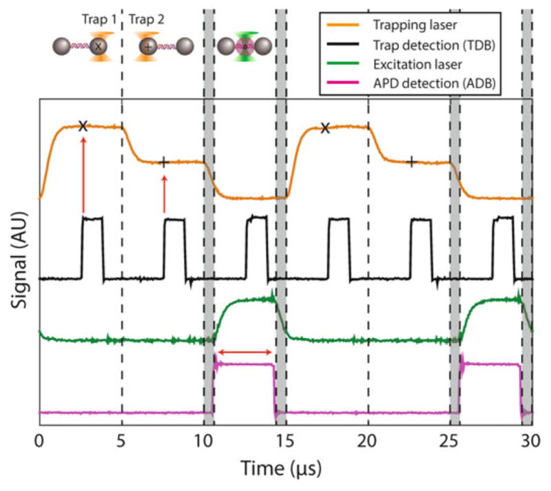
Interlacing and timesharing of optical trap and fluorescence excitation lasers, and synchronization of lasers with data acquisition timing. Two optical traps (orange) are created in sequence during two thirds of the interlacing period by time-sharing. The trap AOM (AOM1) switches between two deflection angles (traps in each interval are set to different intensities for clarity in the figure). Trap data acquisition occurs at time points centered on each trap interval. “×” and “+” denote the time points for the first and second trap, respectively. The rising edge of a digital pulse (black) is synchronous with the trap data acquisition timing (red vertical arrows). The fluorescence excitation (green) is only ON during the last third of the interlacing period while the trap is OFF. There are 625-ns delays (grey shaded regions) between turning OFF (ON) the optical traps and turning ON (OFF) the fluorescence excitation. A digital pulse (magenta) synchronous with the APD data acquisition timing is centered on the excitation laser interval. Fluorescence emission signals are only collected during this third time interval (red horizontal arrow). Laser intensities in the plot are measured by feedback photodetectors QPD1 and PD (see Fig. 3), and digital pulses synchronous with data acquisition timing are output directly from the DAQ card trap input timing debug (TDB) and APD gate timing debug (ADB) lines (see Fig. 10). All are recorded using a digital oscilloscope
We note that acousto-optic deflectors (AOD) are more commonly used for beam steering than modulators. AODs work by the same principle as AOMs, but have been optimized to provide a larger deflection range. However, we have found that AODs adversely affect the quality of the trapping beam and also introduce fluctuations in beam power over small deflection angles. These can affect trap performance. We thus use an AOM to control temporally both the trapping beam intensity and deflection angle. The price of using an AOM is a smaller beam deflection range. We note that all acousto-optic devices exhibit some degree of variation in diffraction efficiency with deflection angle (Fig. 6a). This is problematic as it means that trap stiffness varies with trap position. To counteract this effect, we implement a feedback system to keep the beam intensity within a narrow range for optimal trap performance. Picking off a small fraction (1–2 %) of the trapping beam after the AOM using a high quality wedged beam sampler (BS1), an IR enhanced photodiode (QPD1) monitors the laser intensity (seeNote 1). The signal from QPD1 is passed to the instrument control system, which then uses a standard Proportional-Integral-Derivative (PID) feedback loop to modulate the RF sound wave amplitude driving the AOM to maintain constant beam intensity no matter where the traps are positioned (see Subheading 2.5). This feedback system is effective in stabilizing laser power fluctuations regardless of source, reducing intensity noise by up to six orders of magnitude (Fig. 6b and c) [16].
Fig. 6.
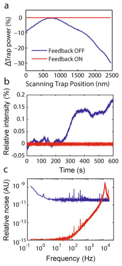
Effect of intensity feedback on trap performance. (a) The trapping beam power changes significantly as the trapping AOM deflects the beam over a range of distances in the specimen plane (blue), but remains constant with feedback ON (red). (b) Feedback stabilizes the trap laser intensity against drift over long time periods (red, feedback ON; blue, feedback OFF). (c) Noise power spectrum of laser intensity. Use of feedback reduces low-frequency noise from the trapping laser by up to six orders of magnitude (red, feedback ON; blue, feedback OFF) (reproduced from ref. [16] with permission from Nature Publishing Group)
The trapping light next passes through two telescopes (T1 and T2), which expand the beam (by 3× and 2×, respectively) to overfill slightly the aperture of the front objective (FO, adjusted to approximately 9 mm beam waist at FO aperture) [29]. The telescopes also make the plane about which the trapping beams pivot inside the AOM conjugate telecentric to the back-focal plane of the objective (denoted by * in Fig. 3). This ensures that deflection of the trapping beam by the AOM produces a displacement of the focused traps in the specimen plane while not clipping the beam on the FO aperture (seeNote 2).
Next, a dichroic mirror (DM1) reflects the trapping light into the front objective (FO). We recommend using a high-quality dichroic that reflects trapping light and transmits fluorescence light efficiently and has a flat surface (<λ/10) and thick (>3 mm) substrate to avoid trap beam distortions prior to entering the objective. FO focuses the IR light, forming the optical traps inside the sample chamber. Considerations for selecting objectives for optical trapping have been described at length elsewhere [26, 29]. Here, we note the use of water-immersion objectives. Oil-immersion objectives generate traps close to the coverslip surface, and the trap stiffness is dependent on the depth of the trap within the chamber. As a result, drift of the surface or focal depth couples to the trap stiffness. An advantage of water- over oil-immersion objectives is that the traps are formed far away from the surface of the flow chamber, where the trap stiffness is decoupled from surface drift, improving stability [26, 32]. However, this comes at a price of a smaller numerical aperture (NA), which leads to moderately weaker traps and affects fluorescence detection (see Subheading 3.5). An identical back objective (BO) is used as a condenser to collect the trapping light. Although an objective is not essential for this purpose, we also use BO as the objective in the bright-field imaging system as it allows directly imaging the traps, which is convenient for alignment (see Subheadings 2.3 and 3.3). An identical dichroic (DM2) reflects the trap light into the detection stage after BO.
Finally, the positions of the beads in the optical traps are monitored by back-focal plane interferometry of the trapping light [33, 34]. In contrast to other groups, we do not use a separate detection laser during normal operating procedures. A relay lens (RL1) collects the light forward-scattered by the trapped beads at the back-focal plane of BO and images it onto a position-sensitive quadrant photodetector (QPD2). QPD2 outputs voltages proportional to the lateral position, x and y, of the centroid of the collected light and to the total light intensity. The positions of the beads in both traps are monitored with the same QPD; which signal comes from which trapped bead is resolved temporally by the data acquisition system (see Subheadings 2.5 and 3.2). The choice of photo-detector is an important consideration in the design of this instrument. At the 1064-nm trapping wavelength, widely used silicon-based position-sensitive detectors (PSD) exhibit parasitic filtering above ~10 kHz [35]. This low-pass filtering leads to signal inaccuracies during interlacing and timesharing at 66 kHz (Fig. 7). We have found that IR-enhanced quadrant photodetectors are accurate at rates >100 kHz at 1064 nm and are essential for proper operation of the instrument.
Fig. 7.
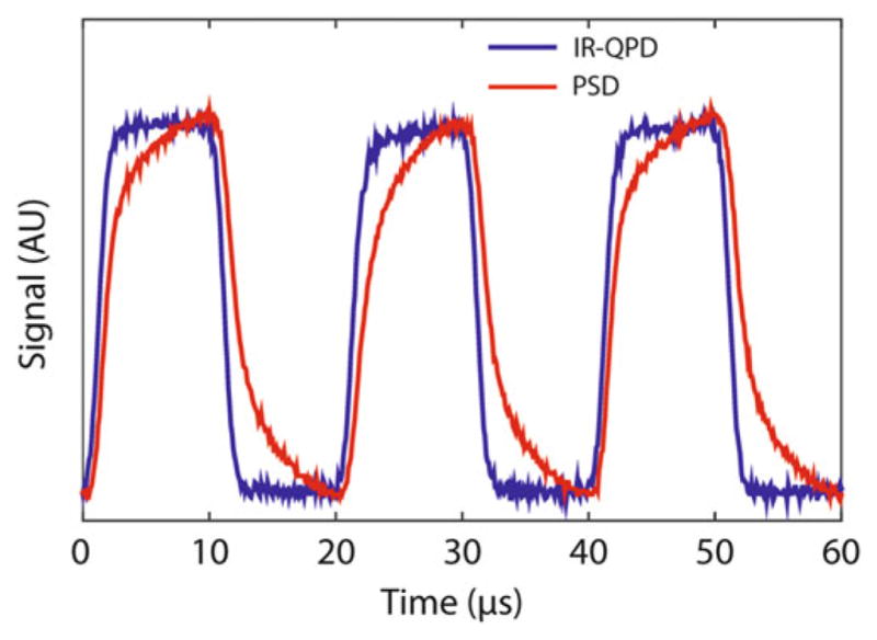
Comparison of IR-enhanced QPD to PSD for IR laser detection. The trapping laser power measured by an IR-enhanced QPD (blue) and PSD (red) during its ON/OFF interlacing cycle is shown. The PSD exhibits parasitic low-pass filtering, characterized by long rise and fall times (reproduced from ref. [16] with permission from Nature Publishing Group)
Components of interest
5-W, 1064-nm fiber laser (IPG Photonics, YLR-5-1064-LP) (seeNote 3).
Fiber clamp (FC; Newport, CCL-1 cable clamp).
1064 nm optical isolator (ISO1; Thorlabs, item formerly from Optics for Research, IO-3-1064-VHP).
1064 nm zero-order half-wave plate (HW1; Newport, 05RP-02-34).
Continuous rotation mount for wave plate (Thorlabs, RSP1).
1064 nm laser line polarizing beam-splitting cube, 12.7 mm (PBS1; Newport, 05BC16PC.9).
Three-axis optic tilt mount for PBS cube (Newport, UGP-1).
Laser beam dumps (2 each: BD; Kentek, ABD-075NP).
1064 nm acousto-optic modulator (AOM) (AOM1; IntraAction, ATM-803DA6B).
Five-axis alignment stage for AOM (Newport, item formerly from New Focus, 9081).
-
Lenses (all are 1064 nm anti-reflection coated, 25.4 mm diameter):
Plano-convex lens, 88.3 mm EFL (L1; Newport, KPX091AR.33).
Plano-convex lens, 250 mm EFL (L2; Newport, KPX109AR.33).
Plano-convex lens, 100 mm EFL (L3; Newport, KPX094AR.33).
Plano-convex lens, 200 mm EFL (L4; Newport, KPX106AR.33).
Bi-convex lens, 150 mm EFL (RL1; Newport, KBX070AR.33).
Iris (Thorlabs, SM1D12C).
Laser line dielectric mirrors, 1064 nm (2 each: M1 and M2; Newport 10Z40DM.10).
Broadband beam sampler, 1010–1550 nm (BS1; Newport, 10Q20NC.3).
Short-pass dichroic beamsplitters, reflected wavelength = 1064 nm, transmitted wavelength = 415–700 nm (2 each: DM1 and DM2; CVI, SWP-45-RP1064-TUVIS-PW-1025-UV) (seeNote 4).
IR-enhanced quadrant photodiodes (QPDs) (2 each: QPD1 and QPD2; First sensor, formerly Pacific Silicon, QP154-Q-HVSD).
Precision stages for QPDs (2: Newport, 460A-XYZ).
60× water-immersion microscope objectives, NA = 1.2 (2 each: FO and BO; Nikon, CFI Plan APO VC 60XWI).
Precision stages for microscope objectives (2 each; Newport, Ultralign 561D-XYZ [right-handed] and 561D-XYZ-LH [left-handed]).
1064 nm laser line filter (F1; Newport, 10LF25-1064).
2.2 Fluorescence Confocal Microscope
Much of the fluorescence confocal microscope module layout is similar to that of the trap, with some important distinctions. A 532-nm 30-mW laser is used for excitation. Although only micro-watts of power are necessary for typical single-molecule confocal microscopy, we also use the excitation laser for alignment (see Subheadings 3.3 and 3.4), which requires increased power.
As shown in Fig. 3, the excitation beam passes through an optical isolator, power stage, and AOM. Here, the AOM only modulates the laser intensity for interlacing with the optical trap. As in the optical trap module, a fraction (approximately 1 %) of the excitation light intensity is diverted (pellicle beam splitter BS2) and monitored by a photodiode (PD) and stabilized via a feedback loop.
Two telescopes (T3 and T4) expand the beam by 4× and 1.3×, respectively (approximately 6 mm final beam waist, slightly less than the FO aperture, to ease the co-alignment of trap and fluorescence beams) (seeNote 5). We recommend using achromatic doublet lenses for all fluorescence imaging in this module to maintain consistent focusing across the fluorescence spectrum. The excitation beam next enters the front objective FO. There are a few important characteristics for the objectives to keep in mind when trapping simultaneously with fluorescence. First, since water-immersion objectives have a lower NA than oil-immersion objectives, the fluorescence collection efficiency in this setup will be slightly lower than that for standard confocal microscopes. Second, chromatic aberrations in FO require adjusting the fluorescence excitation beam collimation so that it is focused in the same plane as the trapped beads. This is achieved via two translation stages that displace the first and second lenses of T3 and T4, respectively, along the optical axis. These provide coarse and fine control over the focal depth of the fluorescence excitation, respectively (see Subheading 3.4). In addition, a piezo-actuated tip-tilt mirror stage (SM) between T3 and T4 is used to adjust the lateral position of the excitation relative to the traps in the specimen plane. The pivot plane of the mirror is made conjugate with the back-focal plane of FO (denoted by ‡ in Fig. 3) by T4.
Fluorescence emission from the excitation focus at the specimen plane is collected by FO, traveling back along the same path as the excitation, but passing through a long-pass dichroic mirror (DM4) and into the confocal pinhole stage. This consists of a telescope (T5), the first lens of which focuses the emission light onto the pinhole (PH, generally 20–100 μm diameter, depending on lens selection and background rejection requirements) (seeNote 6) that rejects out-of-focus light, and the second of which collects the transmitted light. The fluorescence signals are monitored by two avalanche photodiodes for measuring donor (APD1) and acceptor fluorescence (APD2). These detect individual photons and output a single digital pulse per photon to the data acquisition system (see Subheading 3.4).
The 532-nm excitation light transmitted through the sample chamber is also collected by BO and imaged onto a position-sensitive detector (PSD). This detection system is used during alignment, utilizing the excitation as a detection beam for a trapped bead for accurate positioning of the confocal spot laterally in relation to the trapped beads (see Subheadings 3.3 and 3.4).
In general, it is best to keep fluorescence and trap modules well-separated and partitioned to prevent stray trap light from reaching the fluorescence detectors and producing a background signal. We recommend enclosing the instrument modules in blackout boxes containing multiple turns to maximize absorption of stray light (Fig. 4).
Components of interest:
532 nm laser (World Star Tech, TECGL-30) (seeNote 7).
532 nm laser mount and coarse adjustment stage (Newport, VB-1).
532 nm optical isolator (ISO2; Thorlabs, item formerly from Optics for Research, IO-3-532-LP).
532 nmzero-order half-waveplate(HW2; Newport, 05RP02-16).
Continuous rotation mount for wave plate (Thorlabs, RSP1).
532 nm PBS cube (PBS2; Newport, 05BC16PC.3).
Three-axis optic tilt mount for PBS cube (Newport, UGP-1).
Laser beam dump (BD; Kentek, ABD-075NP).
532 nm AOM (AOM2; IntraAction, AOM-802AF1).
AOM driver electronics for excitation laser (IntraAction, ME-801.5-6).
Pellicle beamsplitter (BS2; Newport, PBS-2C).
Iris (2 each; Thorlabs, SM1D12C).
QPD or non-position-sensitive photodiode (PD; QPD: First sensor, QP154-Q-HVSD. Non-position sensitive photodiode: Thorlabs, PDA36A).
Motorized filter flip mount (ND1; Thorlabs, MFF101).
Assortment of neutral density filters (ND1 and ND2; e.g., Thorlabs, NE05A).
Laser line dielectric mirrors, 532 nm (5 each: M5, M6, M7, M8, and M9; Newport, 10Z40DM.11).
Compact linear lens positioning stages for coarse and fine positioning of fluorescence confocal depth (2 each; Newport, item formerly from New Focus, 9066-COM) (seeNote 8)
-
Lenses (all are 430–700 nm anti-reflection coated, 25.4 mm diameter unless otherwise stated):
Visible achromatic doublet lens, 100 mm EFL (L5; New-port, PAC052AR.14).
Plano-convex lens, 100 mm EFL (L6; Newport, KPX094AR.14).
Visible achromatic doublet lens, 150 mm EFL (L7; New-port, PAC058AR.14).
Visible achromatic doublet lens, 50.8 mm diameter, 200 mm EFL (L8; Newport, PAC087AR.14).
Bi-convex lens, 150 mm EFL (RL2; Newport, KBX070AR.14).
Visible achromatic doublet lens, 50.80 mm EFL (L9; Newport, PAC040AR.14).
Plano-convex lens, 25.4 mm EFL (L10; Newport, KPX076AR.14).
-
Dichroic mirrors:
532 nm long-pass dichroic mirror (DM4; Semrock, LPD02-532RU-25).
532 nm short-pass dichroic mirror (DM5; CVI, SWP-43-RU532-TUVIS-PW-1025-C) (seeNote 9).
590 nm edge dichroic mirror (DM6; Chroma, 590dcxr).
Two-axis piezoelectric mirror tip/tilt actuator (SM; Mad City Labs, Nano-MTA2 Invar).
Three-axis tip/tilt mount for piezoelectric mirror (SM; New-port, item formerly from New Focus, 9411).
QPD or position-sensitive detector (PSD) (PSD; QPD: First Sensor, formerly Pacific Silicon, QP154-Q-HVSD. PSD: First Sensor, DL100-7-PCBA3).
Precision stage for PSD (Newport, 460A-XYZ).
-
Filters:
Mounted precision pinhole (PH; e.g., Thorlabs, P100S).
Precision three axis translation stage for pinhole (Newport, 461-XYZ-M).
Avalanche photodiodes (APDs) (2 each: APD1 and APD2; Excelitas, formerly PerkinElmer, SPCM-AQRH-14).
Precision stages for APDs (2 each; Newport, 460A-XYZ).
2.3 Bright-Field Imaging System
The instrument is equipped with a bright-field imaging system (Fig. 3 and 4) that serves two purposes: (1) to visualize directly the sample chamber and beads during experiments, and (2) to image the trap and fluorescence excitation laser beams during some alignment protocols. The specimen plane is imaged by an IR-enhanced CCD camera using Kohler illumination from a blue LED (seeNote 13). Band-pass filters on flip mounts are used to cut out IR trapping and green excitation light during normal instrument operation. The camera signal is recorded and displayed on the instrument computer using a frame-grabbing PC card. PCI-express video cards such as the one listed below should be used, as they provide sufficient data bandwidth to maintain a continuous video stream without interfering with other instrument measurements and control operations.
465 nm blue LED (LED; e.g., Kingbright, 604-WP7113VBC/D).
Visible mirror (M4; Thorlabs, PF10-03-P01).
Bi-convex lenses, 25.4 mm diameter, 200 mm EFL (2 each: L11 and TL; Newport, KBX076).
1000 nm shortpass filter (F2; Thorlabs, FES1000).
532 nm single-notch filter (F3; Semrock, NF01-532U-25).
IR-enhanced CCD camera (CCD; Watec, WAT-902-B).
Frame-grabbing PC card (Matrix Vision, mvDELTAe-BNC).
Video monitor with BNC inputs for viewing inside instrument room (e.g., Ganz, ZM-L17A, distributed by Reytec).
Reticle calibration stage micrometer (Edmund Optics, 59–280).
2.4 Trap AOM RF Synthesis
The trap laser intensity and deflection angle are both controlled via AOM. Since the sound wave that determines both is driven by an RF source, precise and stable RF generation is key for stable, high-resolution trapping. Although the AOM RF signal can be produced from an integrated commercial source, we have found that an RF synthesizer custom-built from a direct digital synthesis (DDS) RF source chip provides much lower noise [16] (Fig. 8). The frequency of the RF output is referenced to a clock signal that must be supplied to the board. The stability of the clock directly affects the stability of the RF output frequency and therefore the stability of trap positioning. The synthesizer itself generates a variable low power signal that we amplify by a low-noise, fixed-gain RF power amplifier to drive the AOM. Care must be taken not to exceed the damage threshold of the AOM with RF power >2–3 W (Fig. 9). A DC-block is inserted inline between the RF synthesizer and amplifier as the amplifier is very susceptible to damage by a DC input. We recommend the following parts to assemble such an RF synthesizer and amplifier. The specifications for the AOM modulating the fluorescence intensity are less stringent, and a commercial RF source is sufficient in this case.
Fig. 8.

Noise power spectra from commercial and custom-built RF synthesizers. The custom-built RF synthesizer (blue) exhibits lower noise than the commercial synthesizer (red) by up to four orders of magnitude (reproduced from ref. [16] with permission from Nature Publishing Group)
Fig. 9.
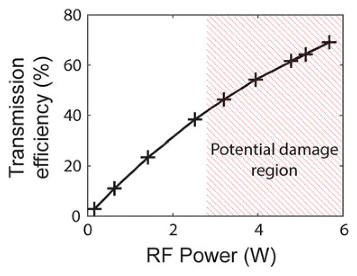
Transmission efficiency of trapping AOM as a function of input RF power. The intensity of the first-order diffracted beam relative to the total intensity input to the AOM increases with RF power. High input RF power can damage the AOM (red hatched region)
Direct digitally synthesized (DDS) integrated circuit (IC) RF source chip on “evaluation” PC board (Analog Devices, AD9852/PCBZ or AD9854/PCBZ).
14-pin DIP, 49.152 MHz fixed output, HCMOS logic, temperature compensated crystal oscillator (TCXO) with 1 ppm stability (Conner-Winfield, HTFL5FG5-049.152 M) (seeNote 14).
14-pin DIP socket.
3.3 V regulated linear power supply for RF synthesizer (Acopian, A3.3NT350).
Standoffs to mount RF board to chassis, 4–40, f-f, 0.375″ long (4 each; e.g., Mouser, 534–2202).
#4 flat insulating washers to mount RF board to chassis (4 each; e.g., Mouser, 534–3368).
40 line ribbon cable (e.g., Mouser, 517–3302/40FT).
40 pin ribbon cable plug (e.g., Mouser, 517–3417–7000).
12″ long SMB plug coaxial test cable (2 each; e.g., Allied, 528–0255).
SMB to BNC adaptor (2 each; e.g., Allied, 319–0409).
BNC jack to jack isolated bulkhead adaptor (2 each; e.g., Allied, 713–8028).
RF synthesizer chassis, 19″ rack box (e.g., Mouser, 563-NHC-14155).
Low-noise, fixed-gain RF power amplifier, 5 W maximum output, 40 dB gain (Mini-Circuits, ZHL-5 W-1) (seeNote 15).
24 V linear regulated power supply for RF power amplifier (Acopian, 24PH15AM) (see Table 1).
Low-noise RF cables (Mini-circuits, CBL-25FT-SMSM+).
DC-block (Mini-circuits, BLK-89 S+).
RFRMSpower meter(Mini-circuits, ZX47-40-S+)(see Note16).
Assortment of RF attenuators (e.g., Mini-circuits, HAT-10+) (seeNote 17).
Combined DPO oscilloscope and RF spectrum analyzer (Tektronix, MDO4000B) (seeNote 18).
Table 1.
Linear regulated low noise DC voltage sources from Acopian
| DB15-10 | +/− 15 V, 100 mA | For the QPD/PSD detectors |
| 5EB50 | 5 V, 500 mA | For wide-field microscope LED |
| A24MT210-M | 24 V, 2.1 A | For NI current analog out control |
| 50EB03 | 50 V, 30 mA | For QPD reverse bias |
| A3.3NT350 | 3.3 V, 3.5 A | For RF DDS synthesizer board supply |
| 24PH15AM | 24 V, 15 A | For RF power amplifier supply |
2.5 Data Acquisition and Instrument Control System
Key components of the instrument, including the trap and fluorescence excitation AOMs, single-photon counting APDs, the bead position measuring QPD, and laser feedback detectors, must be controlled and synchronized to trap interlacing with μs-level precision. PC-based data acquisition (DAQ) cards have historically been unable to achieve this level of timing and control easily, suffering from operating system interference. However, recent Field Programmable Gate Array (FPGA)-based PC DAQ cards circumvent this problem by moving all key timing operations from the PC “host” to a programmable chip on the DAQ card. The FPGA chip runs precisely and consistently as programmed with 40 MHz (25 ns) timing resolution and is isolated from interference from the PC. The FPGA is the “brain” behind all time-sensitive instrumentation control and data acquisition. Data are transferred from the FPGA to the host PC for non-time critical operations such as data analysis, plotting, and saving (seeNote 19 for computer build). Custom LabVIEW (National Instruments) software is used to control the instrument and is separated into FPGA and host PC portions (seeNote 20).
Figure 10 displays the input/output architecture of the FPGA and all the components with which it communicates. There are eight synchronously sampled analog input (AI) channels in total: the x, y, and sum voltages of QPD2 that monitors the trapped bead positions; the x, y, and sum voltages of PSD that monitors the fluorescence excitation beam during alignment protocols; and two sum voltages from the trap and fluorescence feedback detectors QPD1 and PD. Note that the first seven channels are measured directly by the FPGA DAQ card AI. However, the fluorescence feedback detector intensity is measured by an additional AI card installed in an expansion chassis. This additional AI card is directly controlled by the FPGA and adds four more independently sampled AI. This design eases future expansion of the number of fluorescence excitation lasers and data channels. Two digital inputs (DI) collect photon pulses from APD1 and APD2. Two analog outputs (AO) control the two-axis steering mirror (SM) that scans the fluorescence excitation laterally in x and y at the specimen plane. A number of digital output (DO) channels are used to communicate with the custom-built RF source that drives the trap AOM (Figs. 10 and 11). Three additional “debugging” DO are used to indicate APD gating (ADB), trap laser (TDB), and fluorescence excitation laser (EDB) AI timing during interlacing synchronization protocols (see Subheadings 3.2, 3.3, and 3.4). One digital output controls a motorized flip mount to insert or remove a neutral density (ND) filter from the excitation beam path to easily switch between fluorescence excitation (low beam intensity) and bead detection beam (high beam intensity) methods (see Subheading 3.3).
Fig. 10.

Input/output architecture of the FPGA-based DAQ card. Thicker lines refer to groups of wires. The FPGA uses 20 DO lines to communicate with the trap RF synthesizer, including six for individual bits denoting the address byte (AD) and eight for individual bits denoting the data byte (DA). The output RF signal from the synthesizer goes to an amplifier and then to the trap AOM. Three separate debugging DO lines (TDB, EDB, and ADB) are used for synchronizing detection input timing with the interlacing cycle (see Subheadings 3.2, 3.3, and 3.4). One of the FPGA-controlled AO lines is used to output an analog fluorescence signal (AFL) for aligning the instrument (see Subheading 3.4). The FPGA controls an additional set of AIO lines in an expansion chassis. This chassis has one AI line used for the fluorescence feedback PD, and one AO line that is used, along with a DO line from the FPGA, to control the fluorescence RF synthesizer
Fig. 11.

Assembled RF synthesizer board. A ribbon cable (bottom, digital lines labeled) and a coaxial cable (FSK, top) carry digital signals to the board directly from the FPGA (see Fig. 10). The temperature-compensated crystal oscillator (TCXO) is mounted to a 14-pin DIP socket on the board. A coaxial cable carries the filtered RF output signal from the board to the amplifier (top left, labeled IOUT1 on board; the second cable is ignored). Power is supplied to the board from a single 3.3 VDC source (bottom left)
The trap AOM RF synthesizer chip is configured in part (e.g., the RF frequency and amplitude output values) by writing digital bytes (data) to specific locations (addresses) in the chip memory (Fig. 12). We utilize the high-speed parallel data communication method (set by PMODE signal (PM) DO line) of the RF synthesizer board. With this method, a single 8-bit byte of information is sent to a single 6-bit address location in a single data transfer cycle. In general, multiple bytes must be sent in sequence to specify the RF synthesizer board configuration fully (e.g., 6 bytes fully determine the RF frequency). Therefore, in order for all RF chip properties to change synchronously, the board employs a buffered memory process whereby changes are made first to an inactive copy of the chip memory (the buffer). Multiple bytes of data are sequentially transferred to the buffer. This is done by first setting data and address DO lines and then sending a TTL pulse to the write (WR) line. After all necessary changes are made, they are all activated simultaneously by sending a pulse to the update clock (UDC) signal line, which initiates a simultaneous transfer of the buffer memory to the active memory (Fig. 12). The reader should refer to the RF synthesizer chip manual for a complete table of address/configuration settings (Table 9 of ref. [36]) for a more detailed description of operation.
Fig. 12.
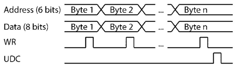
Scheme for writing data to RF synthesizer board. Multiple bytes of data are sequentially transferred to a buffer by setting data and address DO lines and then sending a TTL pulse to the write (WR) line. After all necessary changes are made, they are all activated simultaneously by sending a pulse to the update clock (UDC) signal line, which initiates a simultaneous transfer of the buffer memory to the active memory
There is one key exception to the above. It turns out that changes in RF amplitude and frequency output from a simultaneous UDC-initiated buffer transfer are not timed sufficiently synchronously for our high-resolution trapping requirements. To compensate for this time delay, we devised a method by which we can invoke two independent FPGA DO lines to time and synchronize RF frequency and amplitude switching independently. We utilize the frequency shift keying (FSK) method of the RF synthesizer chip, whereby two separate RF frequencies can be stored on the chip (serving as the “active” and “inactive” trap) and the RF output can be switched between the two frequencies using the RF chip FSK digital input. We specify the next trap frequency in the “inactive” memory location and the amplitude in the usual buffer and control the switching of frequency via the RF chip FSK input and the amplitude via the usual RF chip UDC input. By specifying a delay in the FPGA timing between the switching of the FSK and UDC, we can synchronize RF frequency and amplitude switching (see Subheading 3.1).
The fluorescence excitation AOM driver is controlled by one AO channel (analog scaling) and one DO (digital gating) channel. Using both the analog and digital controls together allows maximally extinguishing the fluorescence beam when it should be off. The analog input of the IntraAction AOM driver we use is low impedance and the analog out channels built into the FPGA DAQ card cannot provide sufficient current to drive it. Therefore we use a special high current analog out card installed in the expansion chassis to provide the analog signal to the fluorescence AOM driver.
It is helpful to use a robust desktop computer with up-to-date multi-core processors (e.g., Intel quad-core i7) and as much memory as possible (32 GB suggested). We also highly recommend using at least two storage drives: a small (e.g., 512 GB) fast solid state drive containing the operating system and all software used (including LabVIEW) and a larger (e.g., 2 TB) conventional hard disk drive (seeNote 21) for saving data. Separating these two drives prevents conflicts during high-speed data acquisition and streaming from the FPGA to the PC and saving to the hard disk.
750 kHz sampling rate FPGA-based multi-function DAQ PC card (National Instruments, NI PCIe-7852R).
C-series expansion chassis (National Instruments, NI 9151).
C-series high current analog output card (National Instruments, NI 9265).
C-series analog input expansion card (National Instruments, NI 9215).
Breakout box (2 each; National Instruments, SCB-68).
Cable to mixed IO breakout box (National Instruments, SHC68-RMIO).
Cable to digital IO breakout box (National Instruments, SHC68-68-RDIO).
Cable to expansion chassis (National Instruments, SH68-C68-S).
Custom LabVIEW software (download here: http://www.pa.msu.edu/people/comstock/software.html).
2.6 Optical Tweezers and Confocal Microscope Alignment
10 μm fluorescent polystyrene microspheres, excitation max = 540 nm, emission max = 560 nm (Thermo, F-8833).
1.0 μm fluorescent polystyrene microspheres, excitation max = 540 nm, emission max = 560 nm (Thermo, F-8820).
1.0 μm fluorescent polystyrene microspheres, excitation max = 535 nm, emission max = 575 nm (Thermo, F-8819).
2.7 Sample Flow Chamber Assembly
Laser engraver (Universal Laser Systems, VLS2.30).
CorelDRAW X4 (CorelDRAW).
1.5 HP portable dust collector motor blower (Penn State Industries, DC3XX).
Dust collection hose and clamps (Penn State Industries, D50C and DBC4).
Movable stage for chamber (Newport, Ultralign 562-XYZ).
Movable stage controller (Newport, ESP301-3N).
Closed loop DC servo stage motors (3 each; Newport, TRA12CC).
Joystick (Newport, ESP300-J).
Remote infuse/withdraw syringe pumps for bead channels (2 each; Harvard, PHD Ultra Nanomite 703601).
Remote infuse/withdraw syringe pump for sample channels (Harvard, PHD Ultra Remote Infuse/Withdraw Programmable 703107).
Microscope coverslips (Fisher, 12-548-5P).
Parafilm M (Pechiney Plastic Packaging, PM996).
Glass capillaries with ID = 0.0250 mm, OD = 0.10 mm (King Precision Glass, custom order).
Anodized aluminum bracket (machined in house, see Fig. 13).
Polished acrylic mounts (2 each; machined in house, see Fig. 13).
4/40 × 1/2″ screws for assembling bracket and acrylic mounts (4 each; see Fig. 13).
8/32 × 3/8″ set screws with 1/16″ holes drilled through centers (8 each; McMaster, see Fig. 13).
26G × 3/8 in intradermal bevel needles (BD, 305110).
Tygon tubing with ID = 1/32″, OD = 3/32″, Wall = 1/32″ (Fisher, ABW00001).
Polyethylene tubing with ID = 0.015″, OD = 0.043″ (BD, 427406).
N-(2-aminoethyl)-3-aminopropyltrimethoxysilane (United Chemical Technologies, A0700).
Methoxy-PEG-succinimidyl valerate, MW 5000 (Laysan Bio, MPEG-SVA-5000-1g).
Fig. 13.

Assembly of laminar flow chamber. (a) Expanded view of the “Parafilm sandwich” that comprises the chamber. A piece of Parafilm with flow channels cut into it is placed on a coverslip with eight holes cut into it. Two glass capillaries span the Parafilm to connect the bottom and top channels to the large central channel. A coverslip with no holes is then placed on top of the Parafilm to form the assembled chamber. (b) A fully assembled flow chamber. (c) A flow chamber mounted on an anodized aluminum bracket, held in place by two acrylic mounts. Four holes on either side of the mount are aligned with the holes of the coverslip. A short length of Tygon tubing is threaded through a set screw, and a longer stretch of polyethylene (PE) tubing is inserted into the Tygon tubing. Eight threaded set screws are prepared and screwed into the eight holes in the aluminum bracket to serve as inlet and outlet channels for the flow chamber. (d) Photograph of an assembled and mounted flow chamber
2.8 Functionalization of Beads
Standard benchtop microcentrifuge with Rotor FA-45-30-11 (Eppendorf, 022620601).
Sample rotator (e.g., VWR, 10136-084).
Analog vortex mixer (Fisher, 02-215-365).
1× PBS buffer (10 mL): 137 mM NaCl, 2.7 mM KCl, 4.3 mM Na2HPO4, 1.47 mM KH2PO4, pH = 7.4.
Protein G-coated polystyrene microspheres, 880 nm nominal diameter (Spherotech, PGP-08-5).
Anti-digoxigenin (Roche, 11333089001).
Streptavidin-coated polystyrene microspheres, 810 nm nominal diameter (Spherotech, SVP-08-10).
2.9 Construction of DNA
Standard thermal cycler for DNA PCR reactions (e.g., Bio-Rad T100, 1861096).
Electrophoresis cell with power supply, 8- and 15-well combs, gel caster, and 7 × 10 cm tray (Bio-Rad Mini-Sub Cell GT Cell and PowerPac Basic Power Supply, 1640300).
UV lamp (Laboratory Products Sales, ENF-240C).
Blue light source gel transilluminator (Clare Chemical Research, Dark Reader Transilluminator DR89X).
Nanodrop 2000 UV-Vis spectrophotometer (Thermo Scientific).
pBR322 vector (New England Biolabs, N3033S).
Lambda phage DNA template (NEB, N3011S).
Primers (Integrated DNA Technology) (see Table 2).
Phusion high-fidelity polymerase PCR master mix (NEB, M0531S).
QIAquick PCR purification kit (Qiagen, 28104).
5× stock of TBE buffer (1 L): 400 mM Tris–HCl, 450 mM boric acid, 10 mM EDTA, pH = 8.3.
6× gel loading dye (NEB, B7021S).
1 kb DNA ladder (NEB, N0468S).
Pre-cast 1 % agarose gels in TBE with ethidium bromide (Bio-Rad, 1613010).
PspGI restriction enzyme (NEB, R0611S).
TspRI restriction enzyme (NEB, R0582S).
UltraPure low melting point agarose (ThermoFisher, 16520-050).
GelGreen nucleic acid gel stain, 10,000× in water (Biotium, 41005).
QIAEX II gel extraction kit (Qiagen, 20021).
T4 DNA ligase (NEB, M0202S).
Table 2.
Oligonucleotides used in example experiment
| Oligonucleotide | Sequence (IDT format, 5′ to 3′) |
|---|---|
| LH forward primer | /5Biosg/TGA AGT GGT GGC CTA ACT ACG |
| LH reverse primer | CAA GCC TAT GCC TAC AGC AT |
| RH forward primer | /5DigN/GGG CAA ACC AAG ACA GCT AA |
| RH reverse primer | CGT TTT CCC GAA AAG CCA GAA |
| Ins | /5Phos/CCT GGT TTT TAG GAC TTG TTT TTT CCC ACT GGC |
| Probe | ACA AGT CCT/3Cy3Sp/ |
2.10 Oxygen Scavenging System/Fluorescence Imaging Buffer
There exist numerous methods for improving fluorescence signal quality in single-molecule experiments, and many of these can be easily adapted for use in these experiments. In particular, oxygen scavenger systems such as the glucose oxidase/catalase mixture are known to increase the photobleaching lifetime of fluorophores [37]. Since singlet oxygen species also tend to cause tether breakage [38], such a system has the effect of improving both tether and fluorophore quality. Additionally, a triplet state quencher like Tro-lox can be used to both prevent fluorophore blinking and photo-bleaching [39].
T50 buffer (50 mL): 10 mM Tris–HCl, 50 mM NaCl, pH = 8.0.
Glucose oxidase from Aspergillus niger (Sigma, G7141).
Pyranose oxidase from Coriolus sp. (Sigma, P4234).
Catalase from Aspergillus niger (EMD Millipore, 219261).
Trolox (Sigma-Aldrich, 238813).
0.22 μm centrifugal filters (EMD Millipore, UFC30GV0S).
0.22 μm syringe filters (EMD Millipore, SLMP025SS).
2.11 Preparation of Beads and Sample for DNA Hybridization Experiment
Gastight glass syringes, 1 mL, PTFE Luer Lock (4 each; Hamilton, 81320).
Fluorescently labeled probe DNA (Integrated DNA Technology) (see Table 2).
3 Methods
3.1 Setup of RF Synthesizer for Trapping AOM
The first component to be assembled and configured is the RF synthesizer that drives the trapping AOM (Fig. 11). An important step in this process is synchronizing the times at which the frequency and amplitude of the RF signal switch. A delay between the RF amplitude and frequency switch will result in a sudden change in one trap stiffness, effectively “kicking” the trapped bead. To avoid this, we require direct and independent timing control of both the RF amplitude and frequency in order to make small timing adjustments to make them synchronous. We do this by tuning a delay into the FPGA timing between the triggering of these two inputs. The proper delay time can be determined by visualizing the RF signal switching directly on an oscilloscope with a sufficient time resolution to resolve individual RF oscillations clearly. This delay time is robust, so this procedure only needs to be performed once.
The following steps describe the assembly of the RF synthesizer board:
-
1
Prepare chassis by drilling holes in bottom panel for RF board standoffs and holes in front panel for signal (RF output and FSK input) and power (3.3 VDC) feedthroughs. We find that the ribbon cable used for digital communication between the FPGA and the RF board can be easily slid out underneath the chassis lid (i.e., no need for a feedthrough).
-
2
Install standoffs on bottom panel of chassis.
-
3
Install BNC signal feedthroughs and banana jack power feed-throughs on front panel.
-
4
Ground yourself with an anti-static strap and perform all RF board assembly work on top of a grounded, anti-static mat. Handle all components by their edges and do not touch component pins or exposed circuitry.
-
5
Mount RF board onto chassis standoffs. Do not over tighten screws.
-
6
Install 14-pin DIP socket onto RF board. Most sockets we have found have all 14 pins, whereas the board only has the 4 corner holes. In this case trim off the inner 10 pins with a wire cutter. Given the tight fit of the socket pins we have installed, we have not needed to solder this connection.
-
7
Install the 14-pin DIP TCXO directly into the 14-pin DIP socket now on the board (see Fig. 11) (seeNote 22).
-
8
Set the jumpers on the board to the following:
W9, W11, W12, W13, W14, W15 jumpers OFF (tri-state jumpers are only set to ON when using the printer port for communication).
W7, W10, W16 jumpers ON (to enable filtered output).
W1, W2, W3, W4, W8 jumpers on the bottom two pins (to enable filtered output).
W17 jumper on the upper two pins (to use the TCXO clock chip).
W6 OFF (to use a single resistor for the output).
-
9
Connect coaxial signal cables between RF board and panel feedthroughs (2 each for RF output and FSK input, use adaptors).
-
10
Connect RF board power inputs to chassis front panel power feedthroughs: first solder wires to panel banana jack feed-through, then screw wires into board inputs. We use a single 3.3 VDC source for all three RF board power inputs.
-
11
Start the RF board by turning on its power supply.
-
12
Initialize (configure) the RF board once after turning it on. This begins with a reset of the board (RESET) followed by a series of digital data transfers using the parallel communications method all performed by the custom LabVIEW software (seeNote 23). Set the following on the board: 6× system clock, phase locked loop (PLL) range low, PLL enabled, output shape keying (OSK) enabled, unramped frequency shift keying (FSK) mode, manual update clock. This RF board reset and initialization is performed whenever the custom LabVIEW software is restarted. The board can remain powered on.
The following steps describe how to synchronize the switching of RF amplitude and frequency for precise interlacing:
-
13
Connect the RF synthesizer output directly to an oscilloscope. Set the scope input impedance to 50 Ω OR use a “T” divider to split the signal between a 50 Ω terminator and the scope set to high input impedance (typically 1–10 MΩ) (seeNote 24).
-
14
Set two easily distinguishable frequencies and amplitudes, corresponding to the two traps. It is easiest to set the second trap amplitude to be ~2× larger or smaller than the first.
-
15
With no programmed delay between the frequency and amplitude triggers, either the frequency or amplitude will typically switch before the other (Fig. 14 middle and bottom panels). Adjust the delay between amplitude and frequency switching until amplitude and frequency switching occur simultaneously (Fig. 14 top panel). 125–250 ns is a typical delay (or 5–10 FPGA clock cycles, for a 40 MHz clock).
-
16
Make this delay the default value in LabVIEW. On startup of the instrument, the amplitude and frequency will be now be synchronized. We have found that this delay remains constant for a given RF board.
Fig. 14.

Synchronization of frequency and amplitude switching of the RF signal. (a) RF signals for the two traps are shown with both frequency and amplitude different by a factor of 2 for clarity (trap 1, 45 MHz; trap 2, 90 MHz). With an appropriately programmed delay between amplitude and frequency signals from the FPGA, the switch happens synchronously (top panel). When there is no programmed delay, the frequency can switch before (middle panel) or after (bottom panel) the amplitude. (b) Traps 1 and 2 during the interlacing cycle, where the RF amplitude is chosen such that both traps have the same intensity. The dotted line indicates when the transition between trap 1 and trap 2 occurs. With the programmed delay between amplitude and frequency switching, the change from trap 1 to trap 2 occurs without any change in intensity (top panel). With no programmed delay, the intensity of trap 2 either drops (middle panel) or rises (bottom panel) to effectively “kick” the bead held in this trap
3.2 Setup of Optical Trap Module
Most of the alignment procedures for the optical trap module have been described in detail previously [26], so we will not repeat these protocols here. The reader can use Fig. 3, which displays a schematic of the instrument drawn to scale, to guide construction of the module. We also refer the reader to the excellent resources on general considerations for aligning optical traps [26, 27, 29]. Here, we focus instead on special considerations required by the use of an AOM and interlacing: how to align the AOM with the trapping beam, how to synchronize trap signal acquisition with the interlacing cycle, and how to locate the plane conjugate to the AOM for positioning the objectives.
Synchronizing data acquisition with interlacing is a particularly important protocol. Since the AOM switches the two traps ON/OFF during the interlacing cycle, measurements of bead positions in each trap must be synchronized with this cycle. Moreover, each bead will be displaced away from the trap center during the OFF cycle of its trap, and will be displaced toward the trap center during the ON cycle (seeNote 25). The pair of trapped beads thus oscillate during interlacing. It is necessary to sample the bead position in the center of each trap ON interval, as it provides the true average bead position (and force) [16] (Fig. 5).
The following steps describe the alignment procedure for the trap AOM. It is important to keep in mind that the first-order diffracted beam coming out of the AOM is the one that will ultimately form the traps, so all alignment must be done for this first-order beam:
-
1
Mount the AOM on the five-axis stage. We recommend machining an adapter plate made of invar or stainless steel to attach the AOM rigidly to the stage, and to minimize drift due to heating of the AOM.
-
2
Elevate the stage using two 1″ height adjustable pedestals for extra stability. Choose pedestal heights such that the trapping beam will pass approximately through the center of the AOM aperture.
-
3
Set the stage to the middle of its range of motion.
-
4
Connect the RF output signal from the synthesizer to a DC block. A DC offset can damage the RF amplifier, so it is important to filter DC signals out.
-
5
Connect this RF signal to the low-noise, fixed-gain RF amplifier.
-
6
Connect the amplified RF output to the trapping AOM using a low-noise RF cable.
-
7
Clamp down the RF cable to the optical table in such a way as to relieve any strain on it. Any shaking of this cable will in turn shake the AOM to which it is attached, so it must be firmly set in place.
-
8
Drive the AOM in the center of its scan range (80 MHz) at low power (~1 W) (seeNote 26).
-
9
Align the AOM by hand such that the trapping beam is roughly centered on the input and output apertures. The beam will pass straight through.
-
10
To achieve an approximate alignment, slowly rotate the angle of the AOM in either direction by hand until a diffraction pattern can be observed coming out of it (see Fig. 15). There are numerous angles that will produce a diffraction pattern, but the optimal angle is the one that produces a pattern with highest intensity. This will be the first angle beyond an incidence angle of 0° as the AOM is rotated either clockwise or counterclockwise (Other sets of diffraction spots will appear if you continue rotating the AOM, and they will be less intense than the first set.).
-
11
Clamp down the base of the AOM stage when this optimal (but still approximate) diffraction pattern appears.
-
12
Place an iris downstream of the AOM to block out all but the first-order diffracted beam. Keep in mind that it is this first-order beam that will ultimately form the traps. Failure to block out the other orders may result in the creation of additional interfering traps.
-
13
Using either a power meter or photodetector to record the output beam intensity, rotate the AOM using the fine-adjustments of the stage until the intensity of the first-order beam reaches a maximum.
-
14
In order to align with the center of the AOM active area, translate the AOM in one of the directions orthogonal to the beam path, finding the two stage positions at which the intensity of the first-order beam reaches half of its maximum intensity (seeNote 27).
-
15
Position the stage in the middle of these two positions.
-
16
Repeat steps 14 and 15 for the other direction.
-
17
Adjust the rotation again to maximize intensity (it is easy to change the angle slightly while translating).
-
18
Attach a ½″ diameter 1064-nm laser line mirror (with very high reflection efficiency) to a post, and deflect the zeroth order beam to a high power beam dump (Fig. 3) (seeNote 28).
Fig. 15.

Diffraction pattern produced by an AOM (either trap or fluorescence AOM). (a) When the AOM is OFF, only the zeroth order (undiffracted) beam is observed. (b) When the AOM is ON, several orders of diffracted beams are observed. The +1 order beam is the one used for trapping
The steps below describe how to synchronize the input timing of the DAQ card with the trap interlacing cycle using the feedback QPD (QPD1 in Fig. 3):
-
19
After the AOM has been aligned, continue to align optics up to the feedback detector QPD1 (Fig. 3).
-
20
Send the total intensity signal of QPD1 to an oscilloscope, and turn on interlacing with both traps ON (seeNote 29). It is best to adjust the amplitudes for each trap to be different so that the center of each can more easily be distinguished (Fig. 5, orange).
-
21
Output from the DAQ card a digital pulse that is synchronous with the analog input timing (TDB line, Fig. 10), and visualize this pulse on the oscilloscope together with the trapping laser intensity signal (Fig. 5, black).
-
22
In LabVIEW, adjust the phase of the analog input timing until it is centered on the trapping laser intervals (seeNote 30).
-
23
Record this phase shift, and set the “initial phase” to this value in the instrument software (make it a default value).
-
24
Upon startup of the instrument, this phase will always be automatically adjusted to the correct value (seeNote 31).
-
25
Trap laser intensity feedback can now be turned on.
The following steps locate the plane conjugate to the trapping laser AOM deflection axis (Fig. 3). The conjugate planes will not be as well-defined when the beam is steered by an AOM instead of a movable mirror. Because there is no true single pivot plane for the deflected beam in the AOM, the conjugate plane will be smeared over a certain distance, typically ½″ for our optics:
-
26
Connect a QPD x, or horizontal, output to an oscilloscope, and center the QPD on the beam near the location you expect the conjugate plane to be.
-
27
Turn off interlacing, and oscillate one trap in the x direction.
-
28
Turn on trap intensity feedback or else the x signal will be difficult to interpret.
-
29
Translate the QPD in the z or axial direction until the oscillations on the scope reach a minimum. They will not reach zero. The conjugate plane will not be sharply defined, so it is sufficient to find the minimum.
3.3 Setup of Fluorescence Confocal Microscope Module: Excitation Laser Path
The following protocol describes the alignment of the fluorescence excitation and emission paths and the synchronization of the excitation and the trapping interlacing cycles (Figs. 3 and 5). It is important to note that all the synchronization and alignment is done relative to the trapping laser, so it is important that the trapping module be optimally aligned before continuing.
The synchronization steps are essential for proper interlacing. Not only must the fluorescence excitation be switched ON during the OFF interval of the traps, but the excitation intensity signal from the feedback detector (PD) and the fluorescence emission signals from the APDs must also be sampled at the appropriate times in the interlacing cycle (Fig. 5). Since fluorescence is only emitted during the excitation laser ON interlacing period, photons should only be counted during this period to reject background. One way to do this is to “gate” the APDs ON/OFF using the APD gate digital inputs. However, we have found that this method often produces false counts, which grow increasingly worse as the APDs age. A preferable option is to keep the APDs ON continuously and instead program the FPGA to record photon counts only during the excitation laser ON interval. The FPGA “recording interval” must still be aligned temporally with the excitation laser ON interval.
The optical alignment procedures include adjusting the lateral (x and y) and axial (z) position of the confocal excitation spot relative to the optical traps in the specimen plane. For a preliminary, coarse adjustment, we use the CCD camera from the visible bright-field imaging system to image the trapping and fluorescence beams. Fine adjustments are made in one of two ways: (1) imaging a trapped fluorescent bead by raster-scanning the confocal excitation across it and using the APDs to record the fluorescence emission, or (2) using the fluorescence excitation as a “detection beam” [29], scanning it across a trapped bead and recording the beam deflection with the PSD. We provide protocols for each option.
The following steps describe how to synchronize the switching of the fluorescence excitation to the trapping laser to achieve precise time-sharing:
-
1
Align the excitation beam path initially without regard to the trapping beam up to the excitation intensity feedback detector (PD, Fig. 3).
-
2
As done previously with the feedback detector for the trapping laser, send the total intensity signal of PD to an oscilloscope (seeNote 29), and turn on interlacing with both the excitation laser and trapping laser ON (Fig. 5, green and orange).
-
3
In LabVIEW, adjust the phase of the AOM interlacing timing until it is positioned between the trapping intervals as in Fig. 5. We set additional 625-ns delays between turning OFF (ON) the optical traps and turning ON (OFF) the fluorescence excitation (Fig. 5, grey shaded regions).
-
4
Record this phase shift, and set the “initial phase” to this value.
-
5
Make this initial phase value the default in LabVIEW. Upon startup of the instrument, this phase will then always be adjusted to the correct value (seeNote 31).
The following steps describe the synchronization of the feedback detector (PD) signal acquisition with the excitation laser during interlacing. Although the excitation laser and trapping laser are synchronized in steps 1–5, the DAQ card will not sample PD at the appropriate time. This problem arises because the analog output of this detector is connected to an expansion input card with a time delay. The procedure is similar to that described above:
-
6
Send the total intensity signal of PD to the oscilloscope, and turn on interlacing with the excitation laser ON (Fig. 5, green).
-
7
Output from the DAQ card a digital pulse that is synchronous with the analog input timing (EDB line, Fig. 10), and visualize this pulse on the oscilloscope together with the excitation laser intensity signal (Fig. 5, green).
-
8
In LabVIEW, adjust the phase of the excitation laser feedback detector analog input timing until it is centered on the excitation laser ON interval.
-
9
Record this phase shift, and set the “Initial phase” to this value.
-
10
Make this initial phase value the default in LabVIEW. Upon startup of the instrument, this phase will then always be adjusted to the correct value (seeNote 31).
-
11
Excitation laser intensity feedback can now be turned on.
These steps describe the coarse alignment of the excitation laser path in x, y, and z relative to the trapping beam using an image of the beam profile on the CCD camera:
-
12
Immediately after the pellicle beam-splitter (BS2), insert a motorized flip mount for adding neutral density (ND) filters. The flip mount is motorized so that the filters can be flipped out of the beam path when the excitation laser is used as a detection laser, which requires high intensity. Adding ND filters here will roughly control the excitation laser intensity. The AOM along with the feedback system provide fine control over the intensity.
-
13
When setting up the steerable mirror (SM), make sure it is set to the center of its scan range (5 V in both x and y directions).
-
14
Center the excitation beam on the front objective (FO) back aperture and make certain it is collimated.
-
15
Translate the front objective stage until the front apertures of both objectives are a few millimeters apart, and place a few drops of water between them.
-
16
Adjust the trap intensity and camera location to visualize the trap in the CCD image as a focused spot.
-
17
Adjust the first movable lens (L5) of the telescope T3 to adjust the excitation laser collimation and roughly focus the fluorescence excitation beam with the trap.
-
18
Roughly co-align the trapping and excitation beams laterally in the x and y directions by observing them on the CCD camera and adjusting the excitation beam angle (using the coarse adjustment stage beneath the steerable mirror) until it is approximately at the same location as the trapping beam. The fluorescence excitation and trap lasers are now roughly focused to the same sample chamber location (laterally and axially).
-
19
Set up the remaining components of the excitation laser path (RL2, M9, and PSD).
-
20
Place the PSD at a plane conjugate to that of the steerable mirror. The procedure for this is essentially the same as that for the trapping laser AOM (Subheading 3.2, steps 26–29), except in this case the procedure must be repeated for both the x and y directions. The conjugate plane should be at the same location for both.
3.4 Setup of Fluorescence Confocal Microscope Module: Emission Path
The following steps describe the alignment of the fluorescence emission path. This requires trapping a fluorescent bead in a flow chamber. Refer to the protocols on assembling laminar flow sample chambers (Subheading 3.9) and mounting the chamber in the instrument (Subheading 3.12) below for details:
-
1
Set up a flow chamber and trap a large fluorescent bead (~10 μm).
-
2
Roughly position the lateral focal spot of the excitation laser on the trapped bead by scanning in the x and y directions with the steerable mirror (SM) and observing the bright spot from fluorescence emission on the CCD camera.
-
3
Adjust the excitation intensity (adjust ND filters and AOM) so that the bead fluorescence emission can be visualized directly by eye. If the room is dark, we have found we can directly observe the emission path for many minutes before the bead photobleaches.
-
4
Align all optics involved in fluorescence detection (everything downstream of dichroic mirror DM4) using the visible fluorescence emission beam from this bead. Leave the pinhole out for now. It may be necessary to trap more than one bead if they bleach too quickly.
The steps below describe the alignment procedure for the APDs. APDs require special care, as the ambient light in a room is intense enough to damage them. As a general rule, APDs should remain off until it is time to make fine adjustments to them, at which point the lights in the instrument room must be turned off:
-
5
Mount the APDs on three-axis precision stages.
-
6
Align the APDs until the fluorescence emission spot from the large beads is visible near the middle of the detector. The APDs must remain off during this step to prevent damage.
-
7
Output an analog signal from the DAQ card that is proportional to the measured fluorescence to the oscilloscope (AFL line, Fig. 10), so the fluorescence signal can be observed in the instrument room during fine adjustment.
-
8
Add ND filters to the motorized flip mount in the excitation laser path, and be sure the filters are flipped in. The intensity of the fluorescence can be high enough to damage the APDs, so it is best to begin with lower intensity (higher ND) and increase it carefully as the need arises. Keep the intensity well below the damage threshold (~1 MHz count rate) at all times (seeNote 32).
-
9
With the lights off in the room, observe the fluorescence signals from the APDs on the oscilloscope. In each direction (x, y, and z) separately, scan the APD across the range of stage positions over which you can observe the fluorescence signal, from minimum to maximum to minimum again. Do not gate the APD: leave it continuously ON.
-
10
For each direction, record the position of the APD stage when the fluorescence signal is at the half-maximum on either side of the range.
-
11
Set the stage halfway between the two half-maxima.
-
12
Once this has been done for the large beads, trap smaller beads (i.e., a bead size that will be used in experiments, typically 1 μm) and repeat APD alignment. This will give a more precise alignment (seeNote 33).
The following steps describe the synchronization of fluorescence signal detection by the APDs with the excitation laser interlacing cycle:
-
13
Create a digital pulse synchronous with the APD measurement ON time (ADB line, Fig. 10) and visualize this on the oscilloscope (Fig. 5, magenta line).
-
14
Trap a 1 μm fluorescent bead, and roughly position the confocal spot in the middle of it using the bright emission spot on the CCD camera.
-
15
Observe the fluorescence signal in LabVIEW, and adjust the phase of the APD measurement ON time until the fluorescence signal just begins to increase. This is the start time of the excitation laser.
-
16
From this point, shift the phase of the APD measurement forward by 3.75 μs (25 % of the interlacing cycle) (seeNote 34).
-
17
Record this phase shift, and set the “Initial phase” to this value.
-
18
Make this initial phase value the default in LabView. Upon startup of the instrument, this phase will then always be adjusted to the correct value (seeNote 31).
The following steps describe how to make fine adjustments to the confocal lateral position relative to the optical traps in the specimen plane. The steerable mirror (SM, Fig. 3) is used to position the confocal spot laterally. The mirror position drifts slowly over time relative to the trap, however, so this procedure must be repeated at the beginning of every experiment (or every 4 h or so). There are two options for this alignment. The detection beam method is usually preferred as it generates a robust image of beads that do not bleach, and is unaffected by particular experimental conditions:
-
19
Set up a flow chamber (see Subheading 3.9) and trap either one bead or a pair of beads, as needed.
Option 1: The following steps use the fluorescence excitation laser as a detection beam and detect its deflection via the PSD as it is scanned across the trapped bead(s).
-
20
Flip out the ND filters to increase the excitation laser intensity. APDs should be OFF!
-
21
Image the trapped bead(s) onto the PSD by scanning the confocal spot in x and y using the steerable mirror (Fig. 16a, b).
-
22
Flip in the ND filters.
Fig. 16.
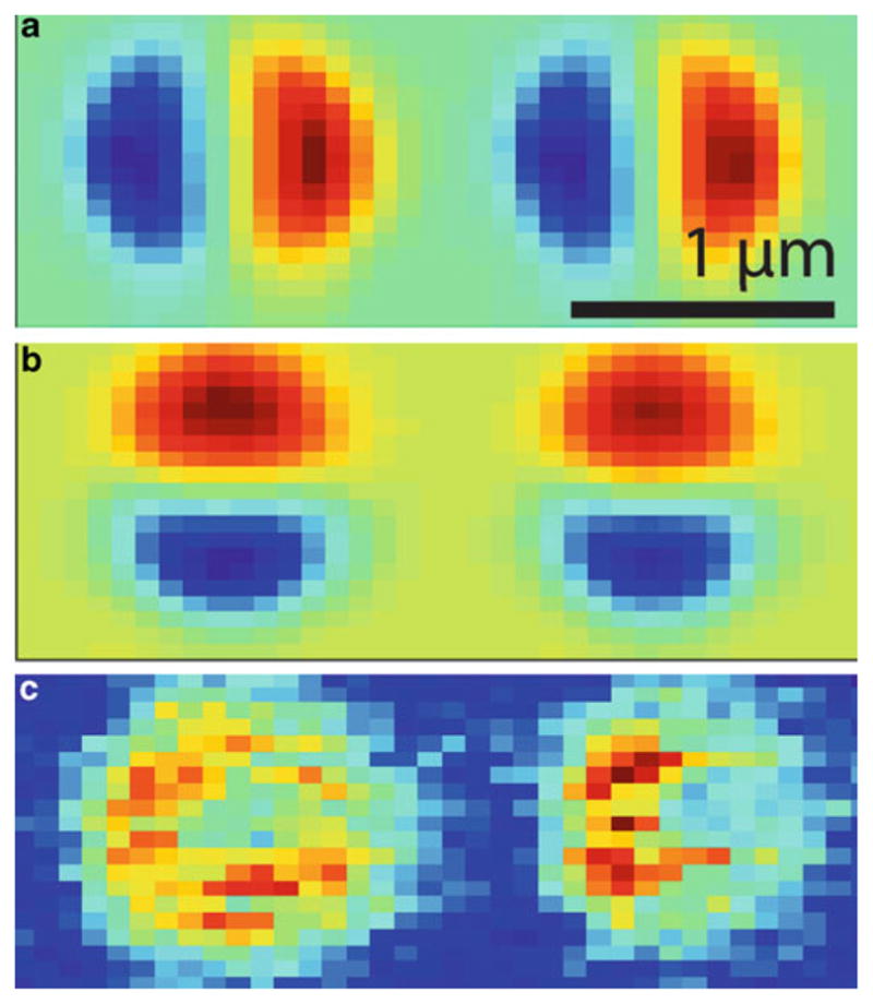
Images of trapped polystyrene beads using fluorescence imaging and detection laser scan. (a) Deflection in the x direction of the fluorescence excitation laser as it is scanned across the two trapped beads. (b) Deflection in the y direction of the excitation laser as it is scanned across the beads (blue denotes negative values; red, positive values). (c) Image of fluorescence intensity of two beads in Trap 1 and 2 recorded by the APDs. The signals result from autofluorescence of the beads (adsorbates can also give a signal)
Option 2: The following steps describe an alternate alignment method using the fluorescence signal from the APDs.
-
23
Image the trapped bead(s) by recording fluorescence using the APDs as the steerable mirror scans in the x and y directions (Fig. 16c) (seeNote 35).
Both options:
-
24
Position the confocal spot laterally with respect to the imaged bead(s) as desired using the steerable mirror (e.g., centered between a pair of beads as for the experiments in Fig. 1).
The axial position (focal depth) of the excitation laser is roughly aligned to that of the trapping laser in Subheading 3.3, steps 12–20. The steps below describe how fine adjustments are made to the focal depth by translating the second movable lens (L8 in Fig. 3) using the translational stage on which it is mounted. Unlike the lateral alignment described above, we find that the axial position does not vary appreciably in time. It is not necessary to repeat these steps before every experiment. There are two ways to find the optimal axial position.
Option 1: Using the fluorescence signal from a fluorescent bead.
-
25
Trap a 1 μm fluorescent bead.
-
26
Set the confocal spot lateral position at the center of the bead by taking a fluorescence image (see step 23).
-
27
Record the fluorescence intensity of the bead at this stage position.
-
28
Adjust the stage position incrementally (usually by 1 mm) and repeat step 27 for each position.
-
29
Plot fluorescence intensity vs. stage position. The optimal stage position is the one that maximizes the fluorescence signal (Fig. 17a).
Fig. 17.

Adjustment of confocal spot focal depth. (a) Relative fluorescence intensity from a trapped fluorescent bead as the focal depth of the confocal spot is scanned (by scanning lens L8 along beam path). The fluorescence intensity drops significantly as the spot is moved away from the plane of the trapped beads. (b) PSD voltage-to-bead position conversion factors, α, derived from calibration using the excitation laser as a detection laser as the focal depth of the confocal spot is scanned. The conversion factors α are minimized when the confocal spot lies in the same plane as the trapped beads. Note: (a) and (b) were not performed for the same instrument alignment and disagree slightly
Option 2: Using the excitation laser as the detection laser to measure the Brownian fluctuations of a nonfluorescent bead.
-
30
Trap a 1 μm bead (nonfluorescent).
-
31
Set the confocal spot lateral position at the center of the bead by taking a detection laser scan (see steps 20–21).
-
32
Leave the ND filters flipped out.
-
33
Perform a trap calibration (see Subheading 3.12, steps 24–25) using the excitation laser as a detection beam, and record the power spectrum of the bead position.
-
34
Determine the conversion factors αx and αy between bead position (in nm) and QPD output (in V) from fitting the power spectrum.
-
35
Plot αx and αy vs. stage position. The optimal stage position is the one that minimizes αx and αy (Fig. 17b). This position will correspond to the highest detection sensitivity, when the confocal spot is aligned in the same plane as the trapped bead.
The following steps describe the protocol for aligning the confocal pinhole:
-
36
Trap a large (10 μm diameter) fluorescent bead.
-
37
Set the confocal spot lateral position by taking a fluorescence image (see step 23).
-
38
Attach the mounted pinhole to its precision three-axis stage.
-
39
Adjust the intensity of the excitation laser so that the fluorescence emission beam is visible by eye on the pinhole mount.
-
40
Shine a small flashlight behind the pinhole so that its location can be easily seen on the other side. The pinhole and fluorescence spot should both be visible.
-
41
Adjust the pinhole stage until the two spots overlap. It may help to start with the pinhole far away from the fluorescence focus so that the beam spot will be large enough to see. The APDs should now be able to detect the fluorescence.
-
42
As done previously (see steps 5–12), output an analog signal from the DAQ card that is proportional to the measured fluorescence to the oscilloscope (AFL line, Fig. 10), so the fluorescence signal can be observed in the instrument room during the fine-adjustment.
-
43
Add ND filters to the motorized flip mount in the excitation laser path, and be sure the filters are flipped in. The intensity of the fluorescence can be high enough to damage the APDs, so it is best to begin with lower intensity (higher ND) and increase it carefully as the need arises. Keep the intensity well below the damage threshold (~1 MHz count rate) at all times.
-
44
With the lights off in the room, observe the fluorescence signals from the APDs on the oscilloscope. In each direction (x, y, and z) separately, scan the pinhole stage across the range of positions over which you can observe the fluorescence signal, from minimum to maximum to minimum again (seeNote 36).
-
45
For each direction, record the position of the pinhole stage when the fluorescence signal is at the half-maximum on either side of the range.
-
46
Set the stage halfway between the two half-maxima.
-
47
Once this has been done for the large beads, trap smaller beads (i.e., a bead size that will be used in experiments, e.g., 1 μm) and repeat steps 43–46. This will give a more precise alignment.
3.5 Adjustment of the Front Objective Correction Collar
Water immersion objectives contain an adjustable “correction collar” to correct for spherical aberrations at the water-cover glass interface. The collar should be adjusted for the sample chamber cover glass thickness to give optimal focus. However, objectives are not perfectly achromatic, such that the optimal settings for the IR trapping laser (1064 nm) will not be quite the same for the excitation lasers (typically 488–633 nm). For high resolution trapping, the correction collar is typically adjusted to minimize the spherical aberration of the trapping laser and to optimize trapping efficiency. Adjusting the correction collar for the trapping laser will, however, ensure that the fluorescence excitation lasers retain some spherical aberration, and thus will decrease the collection efficiency of the fluorescence (Fig. 18). Thus, a compromise is needed between trapping efficiency and fluorescence detection efficiency. We have found that optimizing for trapping or fluorescence efficiency does not usually substantially affect the other. However it is prudent to check both the trapping efficiency and the fluorescence detection efficiency as a function of correction collar setting.
Fig. 18.
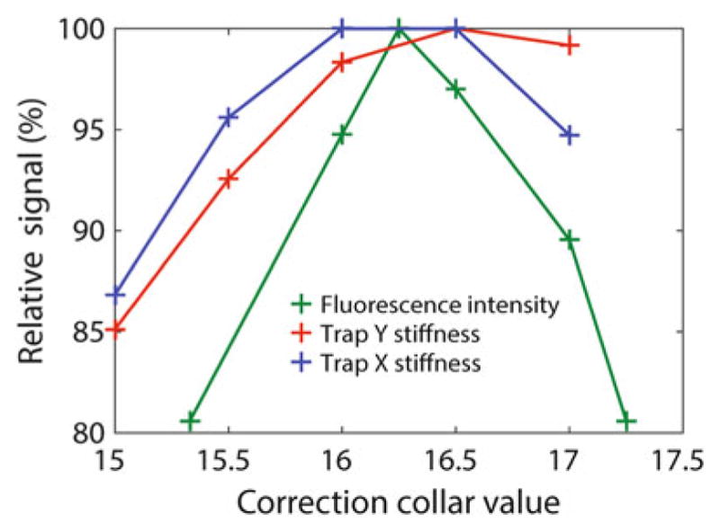
Adjustment of front objective (FO) correction collar (collar shown in Fig. 20a). Relative fluorescence intensity and trap stiffnesses in the x and y directions from a trapped fluorescent bead as the correction collar is adjusted. The fluorescence intensity and trap stiffness do not reach a maximum at the same collar position likely due to chromatic aberrations in the objectives
Set the correction collar to 16.25. #1 coverslips are ~130–170 μm thick, so this is a good starting point.
Trap a small fluorescent bead the same size as used in experiments (1 μm diameter typical).
Set the confocal spot lateral position to the center of the bead by taking a fluorescence image and adjusting the confocal spot (see Subheading 3.4, step 23). If the collar is close to its optimal position for fluorescence detection, the image of the bead will appear circular. If not, the image will be distorted, appearing diagonally elliptical.
Record the fluorescence intensity at this collar position, and save the fluorescence image of the bead.
Perform a calibration of the trap (see Subheading 3.12, steps 24–25) and record the trap stiffness in the x and y directions.
Repeat steps 4 and 5 as correction collar position is varied.
Plot the resulting fluorescence intensity and trap stiffness vs. collar position (Fig. 18) (seeNote 37).
Set the collar position to optimize either the trap stiffness or the fluorescence signal, depending on the demands of the experiment being done. Our typical setting for #1 coverslips is 16.25.
3.6 Calibration of Trap and Confocal Spot Positioning
In the following protocol, we describe how to determine the separation between the traps and the confocal excitation location in the specimen plane in nanometers.
The following steps calibrate the visible imaging system:
-
1
Place a stage micrometer (a linear, constantly spaced 10 μm grid works well) between the objectives in the location usually occupied by the sample chamber.
-
2
Record an image of the grid using the CCD camera.
-
3
Determine the grid spacing in units of image pixels:
Using thresholding, convert the image into a binary image (grid bars and the gaps in between convert to black and white bars, respectively).
Find the centroids of each white bar.
Plot the measured centroid positions (in pixels) vs. the known centers of the bars (e.g., 10 μm between bars).
Fit a line to the data. The slope of the line is the best value of the pixels-to-distance (μm) conversion factor.
-
4
Rotate the stage micrometer 90° and repeat for the orthogonal direction.
The following steps describe how to calibrate the fluorescence steerable mirror (SM) position:
-
5
Set up a flow chamber (see Subheading 3.9).
-
6
Take images of the fluorescence excitation beam on the CCD camera at different SM x and y positions.
-
7
Using image analysis software, locate the beam center in each of the images as a function of SM x and y voltage; e.g., crop the image around the beam spot, threshold to produce a binary image, find the centroid of the bead image.
-
8
Determine the V-to-nm conversion factor from the slope of a linear fit of the beam center positions vs. x and y mirror voltage. Typical values are ~1000 nm/V in x, ~500 nm/V in y.
The following steps describe how to calibrate the trap position:
-
9
Set up a flow chamber (see Subheading 3.9) and trap a 1 μm bead.
-
10
Take images of the trapped bead using the CCD camera at different trap positions.
-
11
Using image analysis software, locate the centers of the trapped bead in each of the images as a function of RF frequency (as above).
-
12
Determine the MHz-to-nm conversion factor from the slope of a linear fit of the bead center positions vs. RF frequency. A typical value for our instrument build is 123 nm/MHz. This value will vary with the specific optical alignment.
3.7 Construction of DNA for Oligonucleotide Hybridization Experiment
This protocol describes how to reproduce experiments described in Comstock et al. [16] (Fig. 1a), which test the fluorescence and trapping capabilities of the instrument by detecting the hybridization of a fluorescently labeled oligonucleotide to DNA tethered between two trapped beads. For this experiment, we synthesize a DNA construct consisting of a short segment of ssDNA flanked by long dsDNA “handles” (Fig. 19). All oligonucleotides used to assemble this construct can be purchased from Integrated DNA Technology (IDT) and are listed in Table 2. We synthesize three DNA segments separately and then ligate them together: left handle (“LH,” 1.5 kb), insert (“Insert,” 19-nt long), and right handle (“RH,” 1.7 kb). LH and RH are made by PCR amplification of sections of the pBR322 plasmid and λ phage DNA using forward primers functionalized with 5′ biotin and 5′ digoxigenin, respectively (Fig. 19). The “probe” that hybridizes to Insert is a 9-nt complementary ssDNA oligonucleotide, labeled with a Cy3 fluorophore on the 3′ end. It is possible to purchase this labeled oligonucleotide directly from IDT. Alternately, labeling can be done in-house using standard amine/NHS ester chemistry [40].
Fig. 19.

Construction of DNA substrate. Schematic depicting the major steps involved in preparing the DNA construct. The handles are first prepared by PCR of template DNA (pBR322 and λ DNA) using primers (FWD and REV) with either a biotin moiety (BIO, Left Handle) or a digoxigenin moiety (DIG, Right Handle) attached to the 5′ ends of the FWD primers. The two handles are digested by restriction enzymes (PspGI and TspRI) to produce 5′ and 3′ overhangs. The digested Left Handle is then ligated using T4 ligase to the short Insert containing a phosphate group on its 5′ end. Finally, the Right Handle is ligated to this product (Left Handle + Insert) to produce the final construct
Steps 1–4 below describe the synthesis and purification of LH and RH:
-
1
For PCR synthesis of LH, mix 35 μL of nuclease-free water, 5 μL of forward primer (10 μM concentration), 5 μL of reverse primer (10 μM), 2 μL of pBR322 template DNA (10 ng/μL), 3 μL DMSO, and 50 μL 2× Phusion HF Master Mix for a final volume of 100 μL.
-
2
For PCR synthesis of RH, mix 35 μL of nuclease-free water, 5 μL of forward primer (10 μM concentration), 5 μL of reverse primer (10 μM), 2 μL of λ DNA (10 ng/μL), 3 μL DMSO, and 50 μL 2× Phusion HF Master Mix for a final volume of 100 μL.
-
3
Run PCR on both reaction mixes, using the following program: (1) 98 °C for 30 s, (2) 98 °C for 10 s, (3) 59 °C for 10 s, (4) 72 °C for 33 s, (5) repeat steps 2–4 30×, (6) 72 °C for 5 min, (7) 4 °C forever.
-
4
Purify PCR products following the QIAquick PCR purification kit “spin protocol.” Add 30 μL of elution buffer instead of 50 μL for a more concentrated solution.
Steps 5–9 below describe the verification of PCR products by gel electrophoresis. These steps are optional:
-
5
Mix 1 μL of each PCR product with 4 μL nuclease-free water and 1 μL 6× gel loading dye.
-
6
Place a pre-cast 1 % agarose gel (in TBE) with ethidium bromide in an electrophoresis cell, and cover it with 0.5× TBE (seeNote 38).
-
7
To this gel, add 5 μL of a 1 kb DNA ladder to lane 1, then 5 μL of the LH PCR product to lane 2, and 5 μL of RH PCR product to lane 3.
-
8
Run at 70 V for ~1 h.
-
9
Image using UV lamp to verify the size of the PCR products.
Steps 10–12 below describe the digestion of LH and RH with restriction enzymes to produce 5′ and 3′ overhangs, respectively. The overhangs are used to base pair to Insert:
-
10
Add to 30 μL of LH: 2 μL of PspGI restriction enzyme and 3.5 μL of CutSmart 10× buffer.
-
11
Add to 30 μL of RH: 2 μL of TspRI restriction enzyme and 3.5 μL of CutSmart 10× buffer.
-
12
Incubate the LH reaction mix at 75 °C for 1 h and the RH reaction mix at 65 °C for 1 h. For convenience, we suggest using a PCR thermal cycler with a temperature gradient of 65–75 °C, so both reactions can be done simultaneously. We program the PCR cycler to 4 °C after 1 h to stop the reaction.
Steps 13–22 below describe the purification of the digestion products using gel electrophoresis. Optionally, these steps can be replaced by purifying the digestion products with a PCR cleanup kit following the QIAquick PCR purification kit spin protocol, adding 30μL of elution buffer for a more concentrated solution (see Note39):
-
13
Add 60 mL of 0.5× TBE to a flask and then add 0.6 g of agarose. Dissolve by briefly heating to a boil in a microwave and swirling.
-
14
Add 6 μL of GelGreen to the solution and mix well (seeNote 40).
-
15
Pour this solution into a gel cast with a 7 × 10 cm gel tray and 8-well comb. Remove any bubbles (dab with the corner of a Kimwipe), then allow it to cool. The solution will solidify into a 1 % agarose gel.
-
16
Place the gel into the electrophoresis cell, and pour 0.5× TBE into the cell until the entire gel is submerged.
-
17
Add 5 μL of 7× gel loading dye to each digestion product, and mix well.
-
18
Add 10 μL of 1 kb DNA ladder to lane 1 of the gel, then all 35 μL of LH digestion product to lane 2, then all 35 μL of RH digestion product to lane 3.
-
19
Run at 70 V for ~1 h.
-
20
Weigh a set of 1.5 mL tubes (write the weights on the tubes).
-
21
Image the gel using the Dark Reader Transillluminator, and cut out the appropriate bands 1.5 and 1.7 kb (for LH and RH respectively) using a clean razor blade. Place these gel slices in the previously weighed 1.5 mL tubes.
-
22
Purify the digestion products from the agarose gel slices using QIAEX II gel extraction kit. Add 30 μL of elution buffer instead of 50 μL for a more concentrated solution.
Steps 23–29 below describe the ligation of LH and RH to Insert. This ligation is done in two steps (LH + Insert first, followed by RH) so that agarose gel purification can be avoided (seeNote 41):
-
23
Measure the concentrations of LH and RH using a Nanodrop, which requires only 1 μL of each solution (seeNote 42).
-
24
Add 4 μL of 10× T4 DNA ligase buffer and 4 μL of T4 DNA ligase to the entire ~30 μL volume of LH. Based on the concentration measured in the previous step, add a 10× excess of Insert. Add nuclease-free water up to a final volume of 40 μL.
-
25
Ligate LH to Insert at RT (~22 °C) for 1 h, and then heat to 65°C for 15 min to inactivate T4 ligase.
-
26
Purify ligation product with a PCR cleanup kit following the QIAquick spin protocol, adding 30 μL of elution buffer.
-
27
Make a solution of this ligation product (LH + insert) and a 2× excess of RH with a final volume of 32 μL, based on the concentrations measured in step 23. Add 4 μL of 10× T4 DNA ligase buffer and 4 μL of T4 DNA ligase to this for a final volume of 40 μL.
-
28
Ligate RH to LH + Insert at RT (~22 °C) for 1 h, and then heat to 65 °C for 15 min to inactivate T4 ligase.
-
29
Optional: gel purify the final ligation product as described in steps 13–22.
3.8 Preparation of Oxygen Scavenging and Anti-blinking Solutions
This protocol describes how to prepare two different oxygen scavenging systems we typically use: one using glucose oxidase (for GOx) [37] and the other using pyranose oxidase (for POx) [41] (seeNote 43). The full oxygen scavenging system includes one of these two enzymes plus catalase and glucose. For long-term storage, glucose is left out of the mixture. We use Trolox (TX) as a triplet-state quencher to reduce fluorophore blinking and photo-bleaching [39].
The following steps describe preparation of the oxygen scavenging systems:
-
1
Dissolve 20 mg of glucose oxidase (for GOx) or 5.8 mg of pyranose oxidase (for POx) and 1.3 mg of catalase into 200 μL T50 buffer (see Subheading 2.10).
-
2
Centrifuge the solution at 13,000 rpm (18,000 rcf) for 1 min to spin down bubbles and any undissolved material.
-
3
Centrifuge solution through a 0.22-μm centrifuge filter at 13,000 rpm for 1 min.
-
4
Store at 4 °C for short-term use (typically a few weeks, watching out for possible precipitation), or aliquot and flash freeze in liquid nitrogen and store at −20 °C for long-term storage (typically months).
The following steps describe preparation of Trolox:
-
5
Add ~8.5 mL of water (seeNote 44) and 50 μL of 1 M NaOH to 10 mL conical tube. The high pH helps the Trolox dissolve.
-
6
Add 10 mg Trolox powder.
-
7
Wrap tube in foil and rotate for ~1 h to dissolve.
-
8
Add 1.10 mL of 1 M Tris–HCl, pH = 8.0 for a final concentration of 110 mM Tris.
-
9
Add water to a total volume of 10 mL.
-
10
Filter the buffer through a 0.22-μm syringe filter.
-
11
Store the Trolox solution in the dark at 4 °C.
3.9 Bead Functionalization
The following protocol describes how to prepare anti-digoxigenin-antibody- and streptavidin-coated beads that link to the digoxigenin and biotin ends of the DNA (Fig. 19). Although the beads come stored in PBS buffer with sodium azide to prevent bacterial contamination, we store beads in aliquots without azide and do not encounter problems with bacteria. These functionalized bead aliquots can be stored for weeks to months at 4 °C. They should never be frozen.
The following steps describe preparation of the anti-digoxigenin (ADig) beads:
-
1
Add 40 μL of 1.0 % Protein G-coated microspheres into 160 μL 1× PBS with 0.01 % Tween 20 (seeNote 45).
-
2
Centrifuge at 7500 rpm (6000 rcf) for 1 min.
-
3
Pipette off the supernatant, taking care not to remove beads.
-
4
Add 200 μL 1× PBS + 0.01 % Tween 20.
-
5
Resuspend pellet by vortexing for 10–30 s.
-
6
Repeat steps 2–5.
-
7
Add 10 μL of 1 mg/mL anti-digoxigenin antibody dissolved in 1 × PBS.
-
8
Rotate on a tube shaker/rotator for 30 min to keep beads in suspension.
-
9
Repeat steps 2–5 twice.
The following steps describe preparation of the streptavidin (Strep) beads:
-
10
Add 40 μL of 1.0 % w/v streptavidin-coated microspheres into 160 μL 1× PBS.
-
11
Spin at 7500 rpm for 1 min.
-
12
Remove supernatant, being careful not to remove beads.
-
13
Add 200 μL 1× PBS.
-
14
Resuspend pellet by vortexing 10–30 s.
-
15
Repeat steps 11–14.
3.10 Assembly of Laminar Flow Sample Chambers
An underappreciated component of optical trap experiments is the sample chamber. A well-designed chamber can significantly improve the throughput of an experiment and allow better control over the system of study. The protocol below describes the design and assembly steps for making laminar flow chambers.
Sample chambers consist of two No. 1 microscope coverslips that sandwich a layer of sealing film into which the channels have been cut (Fig. 13). The top and bottom channels usually contain streptavidin and anti-digoxigenin beads, respectively, and are each shunted to the central channel by thin glass capillaries. Flow in the top and bottom channels causes beads to flush into the central channel, where they are captured by the optical traps. In this protocol, we describe a chamber design in which the central channel contains two adjacent flow streams (Fig. 21). Since the flow is laminar, the two streams do not mix but rather maintain a narrow, stationary interface limited only by diffusion [42]. This chamber design allows rapid exchange of solution conditions by translating the optical traps across the flow interface [43]. This can be used to assemble protein–nucleic acid complexes in situ [14, 22, 23, 44]; for example, loading a motor protein on DNA, then adding ATP in a controlled temporal sequence.
Fig. 21.

Laminar flow cell layout sequence of steps in trap + fluorescence measurement. The flow chamber consists of top (yellow) and bottom (green) channels in which anti-digoxigenin (ADig) and DNA-coated streptavidin (DNA) beads flow, and a central channel comprised of two parallel laminar flow streams containing “blank” buffer (red) and the sample (blue). (Food dye was used in the photograph to show the different channels.) Within the flow chamber, ADig beads flow through the top channel (yellow) and out of the top capillary (black vertical lines) into the sample stream (blue), where it is captured by trap 1 (position 1). The chamber stage is then translated such that the trapped bead remains in the blank buffer stream (red) and is positioned near the bottom capillary (position 2). Here, DNA-coated streptavidin beads (DNA beads) are flowed through the bottom channel (green) and out of the bottom capillary, where one of them is captured by trap 2. When both beads are trapped, the stage is translated until the trapped beads are upstream of the capillaries (position 3). Here the traps are first calibrated, then an offset curve is taken (see Subheading 3.11). The trapped beads are then moved close to one another to form a single DNA tether. A F-X curve is taken to verify proper elastic behavior of the tethered molecule. Finally, the stage is translated such that the trapped beads are moved into the sample stream, which contains 1 nM fluorescently labeled oligonucleotide (position 4). At this position the excitation laser (green cone) is turned ON, and the binding and unbinding of oligonucleotides is observed both by the fluorescence signal and the change in extension of the traps. Whenever possible during this sequence, solution is flowed in the two central streams in order to maintain laminar flow (photo reproduced from ref. [14] with permission from eLife Sciences Publications)
We utilize a computer-controlled CO2 laser engraver to etch inlet and outlet holes into the front coverslip and to cut channels into the film. Although it is possible to do the latter manually with a razor blade, the engraver system allows more elaborate chamber designs that would be difficult to render otherwise. The hole and channel designs are input into a drawing program (e.g., Corel-DRAW) and then “printed” to glass and Parafilm by the engraver, respectively. The details of this process are discussed in the protocol.
Once assembled, the sample chamber is mounted on a custom-built U-shaped aluminum bracket (Fig. 13). Two acrylic mating pieces press the chamber against the two edges of the bracket, aligning holes tapped for 8–32 screws with the inlet and outlet holes of the front coverslip surface. Short pieces of Tygon silicone tubing are fed through machined 8–32 set screws in which the cores have been removed; these are gently screwed into the sample mount, pressing the silicone tubing end onto the inlet and outlet holes of the chamber, forming a seal. Polyethylene tubing is fed into the exposed silicone tubing end and used to flow solutions into the chamber.
The bracket is in turn mounted to a motorized precision x-y-z linear translation stage. The motors allow the translation of the chamber relative to the traps and the positioning of the traps anywhere within the flow channels. The motors also allow this positioning remotely from outside the instrument room. Key sample chamber locations, e.g., the exits of the capillaries out of which beads are flushed, are saved in the instrument software. The chamber can be translated to those recorded positions automatically. We also utilize a joystick to move the chamber relative to the traps manually, e.g., when capturing individual beads in the traps.
The following steps describe how to cut inlet and outlet holes in a coverslip:
-
1
Prepare a batch of coverslips for engraving. It is convenient to prepare ~15 coverslips at a time using a jig that holds an array of coverslips.
-
2
In CorelDRAW, make a blueprint of the arrayed coverslips with holes like the one shown in Fig. 13.
-
3
Set the following settings for the engraver: Power 15 %, Speed 10 %, PPI 250, Z-Axis 4″ (seeNote 46).
-
4
Connect the exhaust from the laser engraver to the portable dust collector blower motor, and the output of this into a fume hood. Turn on the motor.
-
5
Align the engraver vertically: insert jig, place vertical alignment tool onto jig, and adjust stage height.
-
6
Align the engraver laterally:
Load the jig with a single coverslip in the upper left corner location.
Run the engraver program and print a single copy of the blueprint. This will etch the glass and reveal the printing offset.
Measure the x–y offset from the desired location using a micrometer (a few mm could occur).
Translate the blueprint to correct for the offset.
Optional: perform another test run on a single coverslip to verify alignment.
-
7
Load the jig with the full set of coverslips.
-
8
Run the engraver program and print 15–20 copies. It will take ~30 min.
-
9
After engraving is finished, clean all coverslips by carefully wiping them by hand with acetone. Check to make sure there are no fingerprints or pieces of dust.
Some biomolecules will tend to adsorb to the surfaces of the chamber. Adsorption may be particularly important if the molecules are fluorescently labeled, as this may increase fluorescence background. To keep molecules in solution, chambers should be passivated with polyethylene glycol (PEG) [23], using a protocol adapted from ref. [45]. Steps 10–14 should follow if the chambers are to be passivated with PEG. Otherwise these steps may be skipped:
-
10
Sonicate the coverslips in acetone for 30 min.
-
11
Rinse the coverslips with water 3× to remove excess acetone.
-
12
Sonicate the coverslips in 3 M KOH for 20 min.
-
13
Rinse with water 5× to remove excess KOH.
-
14
Rinse once with methanol, and dry with nitrogen gas.
The following steps describe cutting channels into Parafilm:
-
15
Cut a 4″ × 4″ square of Parafilm and place it taut over a frame. We use a machined square metal frame and tape the Parafilm over it.
-
16
In CorelDRAW, make a blueprint of the flow channels as shown in Fig. 13.
-
17
Set the following settings for the engraver: Power 9 %, Speed 10 %, PPI 500, Z-Axis 4″.
-
18
Connect the exhaust from the laser engraver to the portable dust collector motor, and the output of this into a fume hood. Turn on the motor.
-
19
Run the engraver program and print one copy.
-
20
After engraving is finished, use tweezers to pull off carefully any loose segments of Parafilm that may be still attached to the channel structure.
The following steps describe how to assemble a flow chamber:
-
21
Use tweezers to carefully lay down the cut Parafilm on the “hole” coverslip, aligning the Parafilm channels with the cover-slip holes (Fig. 13). It is important to attempt to do this correctly the first time, as moving the Parafilm around tends to leave residue on the coverslips.
-
22
Use a fresh, clean razor blade to cut two glass capillaries to a length such that they will span the Parafilm between the outer channels and the inner channel (seeNote 47).
-
23
Use tweezers to place the two capillaries at the appropriate positions on the Parafilm (seeNote 48).
-
24
Lay the uncut coverslip on top of the Parafilm to form a “Parafilm sandwich” between the two coverslips (see Fig. 13).
-
25
Preheat a hot plate and a ~0.5 kg weight before use to ~100–130 °C (seeNote 49).
-
26
Melt the Parafilm by laying the assembled chamber on the hot plate between two Kimwipes (to prevent melted Parafilm from sticking to the hot plate) with the weight on top of it. Wait ~2–3 min for the Parafilm to melt. It is important that the weight is well centered to apply a uniform pressure over the chamber, otherwise one side will become flatter than another.
-
27
Take the chamber off the hot plate and allow it to cool for ~1 min.
-
28
Mount the chamber onto its bracket, lining up the chamber holes with the bracket holes (see Fig. 13). Gently screw the mounts into place to secure the chamber position (seeNote 50).
-
29
Cut a sufficient length of Tygon tubing for all input/output interfaces (typically 5/8″ per input/output), cutting one end of it diagonally into a point to ease the next step.
-
30
Thread the Tygon tubing into the set screw, leaving sufficient space between the tubing ends.
-
31
Carefully cut the Tygon tubing between the set screws using a new razor blade, making sure the cut is straight (seeNote 51).
-
32
Cut a sufficient length of PE tubing (7–10″ typically), and push it into the Tygon tubing.
-
33
Gently screw the set screws into the chamber bracket until the Tygon tubing is flush up against the chamber (seeNote 52).
-
34
Insert 26-gauge 3/8″ intradermal bevel needles (brown package) to the input PE tubing (seeNote 53).
Steps 35–48 should follow if the chambers are to be passivated with PEG. Otherwise these steps may be skipped:
-
35
Sonicate a 125 mL Erlenmeyer flask in 1 M KOH.
-
36
Rinse the flask with water 3× to remove excess KOH.
-
37
Sonicate the flask in methanol for 20 min.
-
38
Rinse the flask with methanol and dry with nitrogen gas.
-
39
In the flask, make a solution of 1 % (v/v) N-(2-aminoethyl)-3-aminopropyltrimethoxysilane and 5 % (v/v) acetic acid in methanol.
-
40
Assemble the flow chamber, then flow 1 mL of the amino-silane mixture through the channels.
-
41
Allow the amino-silane mixture to incubate for 15 min.
-
42
Flow another 1 mL of the mixture, and incubate for 15 min.
-
43
Flush out the amino-silane mixture with 1 mL methanol.
-
44
Flush out the methanol with 3 mL water.
-
45
Make a solution of 25 % (w/v) methoxy-PEG-succinimidyl valerate in 0.1 M sodium bicarbonate.
-
46
Flow ~200 μL of this PEG solution into each channel.
-
47
Allow the chamber to incubate for ~4 h, then rinse with copious amounts of water and dry with nitrogen gas.
-
48
Store PEG chambers in 4 °C in the dark.
3.11 Preparation of Beads for Experiment
In this section we describe how to prepare DNA beads. We find that the DNA does not remain very stable on these beads, and so typically perform a fresh incubation at the start of each experiment.
Add 1 ng of the DNA construct to ~8 ng of Strep beads.
Incubate at RT for ~1 h for biotin-streptavidin bonds to form.
When Strep + DNA beads are ready, prepare four sample syringes by wetting the plunger and syringe interior with distilled water and then inserting the plunger. Attach needles to the ends.
DiluteADigbeads~1000×intoT50buffer(seeSubheading2.10), and extract ~400 μL into a labeled syringe (seeNote 54).
Dilute Strep + DNA beads ~100× into T50 buffer, and extract ~400 μL into a labeled syringe.
3.12 Sample Buffer Preparation for Oligonucleotide Hybridization Experiment
The buffers described below should also be prepared fresh for each experiment. The final buffer should be: 100 mM Tris (pH = 8.0), 100 mM NaCl, the oxygen scavenging system (1 % glucose, 1 mg/mL glucose oxidase or 0.29 mg/mL pyranose oxidase, and 0.065 mg/mL catalase), and the triplet state quencher to prevent fluorophore blinking (1 mg/mL Trolox). One of the samples contains 1–10 nM of the fluorescently labeled oligonucleotide, while the other does not.
In a 1.5 mL tube, mix 789 μL of TX buffer (see Subheading 3.8), 43 μL of filtered 20 % (w/v) glucose, and 17 μL of filtered 5 M NaCl.
Split this buffer into two aliquots of 392 μL.
In one aliquot, add 4 μL of 1× TE buffer. This is the “blank” buffer.
In the other aliquot, add 4 μL of the appropriate concentration of the oligonucleotide probe (typically 1 μM, in 1× TE buffer). The final probe concentration should be 1–10 nM. This is the sample buffer. Keep in the dark.
Add 4 μL of GOx or POx to each tube.
Mix each solution well, and extract them into their respective syringes.
3.13 Setting Up the Instrument for an Experiment
The following steps describe the instrument startup procedure. Note that the order is important:
-
1
Turn on the RF amplifier. Very important: the RF amplifier power should always be turned on before any signal is sent to it, i.e., before the RF synthesizer power is turned on. Otherwise the amplifier may be damaged. Similarly, when shutting down the instrument, the RF synthesizer power should be turned off before turning off the RF amplifier power. The best practice is always to turn the RF amplifier power on/off as the first/last step.
-
2
Turn on all other power supplies, except for the APDs (seeNote 55).
-
3
Run LabVIEW program. It is important that the RF synthesizer board is already on at this point since the program initializes it.
The next steps prepare the sample chamber for measurement:
-
4
Starting with the center channel, flow several hundred μL of 0.22-μm syringe filtered 20 mM Tris buffer through, until the channel is filled and liquid comes out the outlet tubing. If using a chamber with multiple streams converging into the central channel, fill all of these simultaneously.
-
5
Check the outputs of the capillaries in the adjoining bead channels for fluid coming out to verify that the capillaries are not clogged (seeNote 56).
-
6
Fill the outer bead channels with 0.22-μm syringe filtered 20 mM Tris buffer.
-
7
Flow enough liquid through to see if there is a leak at the inlet and outlet tubing (seeNote 57).
-
8
Verify by eye that there are no bubbles visible in the central channels. If there are, most can be pushed out with more buffer flow (try pulsing) or dissolved as buffer flows over them.
The following steps describe installation and alignment of the chamber in the instrument. A video monitor connected to the bright-field imaging CCD is used to check chamber alignment. It is important to adjust the chamber tilt angle for best trap performance:
-
9
Locate the camera CCD sensor at the focal plane of the tube lens (TL, 8″). At this position, the correctly collimated trap beam will appear focused.
-
10
Retract the front objective (FO) so the chamber can be placed between it and the back objectives (BO).
-
11
Mount the chamber on its motorized stage, a short distance (<1 mm) from BO (seeNote 58), lining up the capillaries of the chamber with the center of BO by eye. The chamber should be mounted loosely so that fine adjustments to its angle can be made later (Fig. 20).
-
12
Place the output tubing in a waste beaker. We recommend submerging it under some buffer, as this helps maintain flow by eliminating evaporation from the tubing ends.
-
13
Rotate the chamber until it looks (by eye) like the plane of the chamber is vertical.
-
14
Move FO toward the chamber, adding a few drops of 0.22 μm filtered water between both objectives and the chamber when they are close enough.
-
15
Adjust FO until the inside surface of one of the coverslips comes into focus on the video monitor. Make sure the trap beam is in the center flow channel and does not pass through Parafilm or capillaries.
-
16
Flip out the IR and excitation laser filters in front of the CCD camera and flip in the ND filter to allow imaging the trapping beam.
-
17
Turn on one of the traps (seeNote 59).
-
18
Move FO until the IR beam comes into focus on the video monitor. The trap should be collimated now. Do not adjust the FO position further. The collimation can be verified by checking that the trap beam profile remains the same size at varying distances beyond BO.
-
19
If the chamber is tilted relative to the beam axis, the beam image will be smeared in y (vertically), i.e., there will be a coma (Fig. 20b, beams slightly out of focus to accentuate smearing). This adversely affects trap performance, adding low frequency noise. Adjust the chamber tilt manually until the beam image on the video monitor is symmetric (Fig. 20c).
-
20
Flip in the IR and excitation laser filters and flip out the ND filter.
-
21
Scan the motorized stage and inspect each bead capillary along its length and verify that there are no bubbles. Bubbles are a common problem that will prevent the flow of beads into the main channel.
Fig. 20.

Alignment of flow chamber to front and back objectives. (a) Photograph of a mounted flow chamber resting on the motorized sample stage via a lens post, with the chamber between the front and back objectives. (b) and (c): Trapping laser beam profiles on the CCD camera when the chamber is misaligned in the y direction (b) and properly aligned (c). (d) and (e): Power spectra of trapped bead motion in y when the chamber is misaligned in the y direction (d) and properly aligned (e)
In the following steps, beads and sample buffers are flowed into the mounted chamber and the trap is checked:
-
22
Attach the syringe with ADig beads to the top bead channel and place it in one of the syringe pumps. Be sure to not add any air bubbles in the process.
-
23
Flush in ADig beads (approximately 100 μL, at a flow rate 100 μL/min). It is helpful to observe the output of the bead capillaries on the monitor when flowing in beads. Beads should be clearly seen streaming out of the capillary.
-
24
Capture an ADig bead with one optical trap, monitor its position using QPD2, and save the data to a file at full bandwidth (66 kHz). Make sure the trap is positioned away from either capillary or cover glass surface as these will distort the trapping beam.
-
25
Determine and plot the power spectral density of the trapped bead position measured in the previous step. We use this standard approach to calibrate the optical traps [29, 46, 47], determining the conversion factors αx and αy (in nm/V) between the photodetector output signals and bead positions and the trap stiffnesses kx and ky (in pN/nm) along x and y. We also use the power spectra to identify alignment errors. Additional low frequency noise (<2 kHz) in the spectra can be caused by chamber tilt relative to the trapping beams (Fig. 20d). Adjust the chamber tilt angle accordingly as described in steps 19–20 above.
-
26
Fix the chamber post rigidly to its stage by tightening the screws.
-
27
Optional: Slightly adjust the camera position until the trapped bead is well focused on the video monitor.
-
28
Attach the syringe with DNA-coated Strep beads to the bottom bead channel and place it in one of the syringe pumps. Be sure to not add any air bubbles in the process.
-
29
Flush in DNA-coated Strep beads into the bottom bead channel (approximately 100 μL, at a flow rate 100 μL/min).
The sample chamber position is controlled by a motorized 3-axis translational stage. We record several stage positions in the LabVIEW software, which allows moving rapidly to commonly used areas in the chamber (e.g., the capillaries, where beads are dispensed). This method increases throughput significantly. The following steps describe how to configure the motor controller settings:
-
30
Move the stage to the Strep bead capillary.
-
31
Choose a convenient location some short distance from the capillary, and zero the stage controller position to (0, 0, 0) (seeNote 60).
-
32
Set other stage positions. We typically record five stage positions in total: by the lower capillary (see previous step) and the upper capillary, where beads are dispensed, within each of the flow streams in the central channel where measurements are taken (for the two-stream channels described here, in the upper and lower flow streams), and at one last position where trapped beads can be released after measurement (seeNote 61).
-
33
Move to the prerecorded position in the stream where the fluorescent sample will be.
In the final experimental setup steps, the fluorescence excitation is turned on and fluorescent sample loaded:
-
34
Make absolutely sure the lights are off in the instrument room, and then turn on the APDs. Generally the instrument black out enclosures should protect the APDs if the room lights are on, but enclosure covers can be inadvertently ajar.
-
35
Turn on the excitation laser and adjust ND filters and AOM to produce ~3 μW of power measured before FO (averaged over interlacing, seeNote 62).
-
36
Attach sample syringes to the central channel.
-
37
Flush 100 μL of sample into the central channel (both center channel syringes are simultaneously injected by the syringe pump) and monitor the APD signals. The background fluorescence should increase and level off as the fluorescently labeled probe fills the channel. This is a helpful measure of the background fluorescence at the start of each experiment. For a well-passivated chamber, the background fluorescence should not drop after the buffer flow stops.
-
38
Switch the center channel flow to a constant rate of 100 μl/h (~140 μm/s linear flow speed) to maintain laminar flow and prevent the blank and fluorescent probe channels from mixing.
In the next steps, the confocal excitation is aligned laterally (in x and y) with the optical traps and positioned where the fluorescence signal is expected. The alignment involves imaging the pair of trapped beads by scanning the fluorescence excitation beam, turned to high power, across the beads and measuring the beam’s deflection using the PSD. These steps must be performed once per trapping session:
-
39
First, be sure the APDs are turned off.
-
40
Flip out the ND filter in the fluorescence excitation beam path using the motorized flip mount to increase the excitation intensity for detection beam scanning.
-
41
Trap a pair of beads.
-
42
Set the separation between the traps to where the traps are expected to be during the experiment.
-
43
Scan the movable mirror SM in x and y to image the pair of beads (Fig. 16).
-
44
Flip back in the ND filter in the fluorescence excitation beam path using the motorized flip mount to reduce the excitation intensity down for single-molecule fluorescence measurements.
-
45
From the image of the beads produced, find the position where the fluorophore is expected to be (centered between the beads for the DNA constructs in Fig. 1), and set the mirror voltage to this value. For the hybridization experiment, this positions the confocal spot at the binding site of the oligonucleotide probe (seeNote 63).
3.14 Measuring Hybridization of Fluorescently Labeled Oligonucleotide
In the following protocol, we describe a simple proof-of-principle experiment using the optical traps and confocal microscopy. The protocol details how to capture beads with the optical traps, calibrate the traps, form a single DNA tether between the beads, take a force-extension (F-X) curve of the tethered DNA molecule, followed by data collection at constant trap separation or constant force (Fig. 21).
The conversion factors between QPD2 voltages and the positions of beads relative to the centers of their traps and the trap stiffness should be determined for each pair of beads during an experiment. We use the standard calibration method, measuring the Brownian fluctuations of the beads in the traps and fitting the power spectral density of the bead positions to the characteristic Lorentzian shape [29, 46]. This fit is used to obtain α, the conversion factor between photodetector signal and physical bead displacement in nm, and k, the stiffness of the optical trap, for each bead and in the lateral directions x and y.
The QPD voltages V are related to the physical bead displacements by x = α(V–Voff)/S, where Voff is a voltage offset from the photodetector, and S is the total intensity incident on the photodetector. Importantly, the offset voltage Voff is not constant across trap positions. There are a few sources contributing to this effect, including the imperfect deflection axis of the AOM (which causes the trapping beam to move across the QPD when scanned), AOM interference effects, cross talk between the two traps, etc. This effect is most pronounced when the traps are close together. In order to measure the correct bead displacement (and force), an “offset curve” must be taken prior to forming a tether to obtain Voff as a function of trap separation (Fig. 22a). The necessity of this procedure is illustrated by comparing F-X curves calculated using Voff values determined at a single trap position (e.g., where the traps are calibrated) vs. one calculated using the separation-dependent Voff values from the “offset curve” (Fig. 22b). Only when Voff values from an offset curve have been subtracted from the QPD voltages are accurate values for the extension and force obtained. We have found that the conversion factors α and trap stiffnesses k do not change significantly with trap separation.
Fig. 22.

Obtaining a force-extension (F-X) curve of a DNA tether. (a) Recorded voltage from the bead position QPD as one trapped bead (in trap 1) is moved relative to the other trapped bead (in trap 2) (i.e., a blank F-X curve). The voltage offset Voff in the QPD output signal for trap 1 (red) and 2 (blue) depends on the separation between the two traps. Offset values obtained at the fixed positions where the traps are calibrated are also shown (× and +). (b) F-X curves of the DNA construct (Fig. 19) with either the “fixed” offset value (black and magenta) or the variable (separation-dependent) offset removed (red and blue). The data recorded from each trap are plotted separately for clarity. Only the F-X curves with a separation-dependent offset removed display the correct behavior. (c) The final F-X curve is plotted with the extensible wormlike chain (XWLC) model [49, 50]. The final F-X curve (cyan) is obtained by averaging the force from traps 1 and 2, where each has its variable offset removed individually. This averaged F-X curve is overlaid on the XWLC model (black dotted line) by shifting the curve along the extension axis by a small, fixed value resulting from uncertainty in the diameters of the trapped beads. The parameters used for the XWLC model for dsDNA and ssDNA are: persistence lengths Pds = 50 nm, Pss = 1 nm, helix rises hds = 0.34 nm/bp, hss = 0.59 nm/bp, and stretch moduli Sds = Sss = 1100 pN [51–53]
The following steps describe how to capture ADig and Strep beads, calibrate the trap, take an offset curve, form a tether, and take a F-X curve:
-
1
Move to the top ADig bead capillary.
-
2
Turn off the central channel flow. This ensures that beads will not be swept away by the flow before they can be trapped.
-
3
Turn on the ADig bead syringe pump at a low flow rate (~100 μl/h is typical).
-
4
Turn on one trap.
-
5
Trap an ADig bead when it comes out of the capillary.
-
6
Turn off the ADig bead pump, and turn the center pump back on (seeNote 64).
-
7
Move to the bottom Strep bead capillary.
-
8
Turn off the central channel pump, and turn on the Strep bead pump.
-
9
Turn on the second trap and set the trap separation to ~18 MHz, corresponding to ~2 μm (seeNote 65).
-
10
Trap a Strep bead in the opposite trap, being careful not to let it fall into the trap holding the ADig bead.
-
11
Turn off the Strep bead pump and turn the central channel pump back on to reestablish laminar flow and wash away any excess beads (seeNote 66).
-
12
Move to a position in the blank channel to calibrate the traps. It is a best practice always to use the same position in the chamber.
-
13
Turn off the central channel pump and acquire trap calibration (seeNote 67).
-
14
It is useful at this point to analyze the calibration power spectra (e.g., in Matlab) to obtain α, k, and Voff for each bead and for both lateral directions, x and y. In this way, the calibration parameters can be input in LabVIEW to view displacements and forces in real-time (seeNote 68).
-
15
Acquire an offset curve by displacing one of the traps relative to the other while recording the bead positions. Scan over a large range in separation to ensure that it covers the range over which data may be taken subsequently (Fig. 22b). In this way, the position-dependent offset can always be subtracted even if subsequent F-X curves have variable ranges.
-
16
Form a tether by moving the beads close together and then apart repeatedly. A tether is detected by an increase in the force on the beads when they are moved apart (seeNote 69).
-
17
Take a F-X curve of the tethered DNA.
-
18
Assess the tether quality by comparing the F-X curve to the theoretically predicted polymer model (see Note 70). It is best practice to reject the bead pair and a new pair of beads captured if a “bad” tether is formed.
Option 1: Collecting a time trace using constant trap separation:
-
19
Move the traps to fixed positions corresponding to the desired tether tension.
-
20
Start saving data.
-
21
Move the tether into the channel containing the fluorescently labeled DNA probe, and turn on (i.e., interlace) the excitation laser and APDs.
-
22
Observe the binding and unbinding of oligonucleotide probes by simultaneous trap detection of changes in tether extension and by fluorescence as in Fig. 1a. The trap signal recorded in this case is the displacement of the beads from the centers of their respective traps (see Note 71). For the 3 μW average fluorescence excitation power, expect to detect ~2 kHz photon rate from a single Cy3 fluorophore.
Option 2: Collecting a time trace using constant force:
Using the force-feedback system, displacements of the beads from their set-point values are compensated by a change in trap position. The displacement of the beads from their trap centers remains constant, and the data of interest are the instantaneous trap separations. Force feedback is achieved through an FPGA-programmed PID controller similar to the intensity feedback (see Subheading 2.1). Differential bead position signals are monitored (i.e., bead 1 position–bead 2 position) and one trap is moved to keep this signal constant. Monitoring the differential bead position increases stability and reduces noise compared to monitoring one bead [9]. Finally, the same trap AOM simultaneously controls both the trapping beam intensity by feedback as well as the trap positions during force feedback. For these two feedback loops not to interfere with each other, we run the intensity feedback as usual at the full 66 kHz interlacing rate while running the trap position feedback 100× slower at 666 Hz.
-
23
Move the traps apart to exert the desired force on the tether.
-
24
Set the bead displacement difference as the feedback set-point value.
-
25
Activate the force-feedback system.
-
26
Move the tether into the channel containing the fluorescently labeled DNA probe, and turn on (i.e., interlace) the excitation laser and APDs.
-
27
Observe the binding and unbinding of the oligonucleotide probe to the tethered DNA construct by simultaneous detection of changes in tether extension and fluorescence as in Fig. 1a. The trap signal recorded in this case is the trap separation (seeNote 72).
Acknowledgments
We thank members of the Chemla, Ha, and Comstock laboratories for scientific discussion. Funding was provided by NSF grants MCB-0952442 (CAREER to Y.R.C.), PHY-1430124 (Center for the Physics of Living Cells to Y.R.C.), RC-105094 (to M.J.C.), and NIH grant R21 RR025341 (to Y.R.C.).
Footnotes
These can be replaced with detectors that do not measure beam position (e.g., Thorlabs PDA36A).
In practice it is impossible to do this perfectly as there is no single pivot plane about which the beams are rotated inside the AOM.
As discussed above, we choose the 1.5 mm collimation option. To minimize noise and heat production in the instrument isolation room, we locate the laser power supply outside the room and route the fiber into the room. Since the optical fiber is the laser cavity, there are limits on the length of the fiber. We have found that a 4 m long fiber works well. We also choose the red guide laser option, which produces a red beam co-aligned with the 1064 nm trap beam. This is a very helpful alignment feature for initial coarse alignment of the laser with the isolator, power modulation stage and the AOM since it avoids the potential of damaging components with misalignment of the high power 1064 nm beam. Note that the red guide beam is not useful after the AOM since it does not diffract with the 1064 trap beam.
This exact mirror is no longer available. It seems that the manufacturer, CVI, will no longer make a mirror with sufficient visible transmission efficiency. As alternates, we have also successfully used similar mirrors from Semrock (NFD01-1064) and Chroma (T970dcspxr). We requested the mirrors be custom cut round with a 25 mm diameter. These two mirrors are not offered on preferable, thick substrates (4–8 mm) so care must be taken to mount the mirror without bending it. We find it best to epoxy these mirrors into the mirror mounts, although alternatives to epoxy are available (see Note 25 in ref. [47]).
It can be challenging to co-align the fluorescence excitation beam with the trapping beam without asymmetrically clipping the fluorescence beam. Making the fluorescence beam waist slightly smaller than the objective aperture makes this procedure easier, with the cost of a slightly larger confocal spot.
Given the fluorescence beam waist and the focal length of the lens imaging the fluorescence onto the pinhole (given above), we commonly use a 100 μm diameter pinhole which achieves a modest amount of background rejection without blocking any fluorescence signal. For many typical applications we have found this to be sufficient. For stronger background rejection with modest signal loss for use in higher fluorescence background, we have found a 20 μm diameter pinhole to be optimal.
This exact laser has been discontinued. However, the exact choice of 532 nm excitation laser is not critical. Any laser with the best beam quality offering 10–50 mW output power should do. The high power is not necessary for fluorescence excitation but rather for use of the laser as a detection beam for alignment purposes. We have successfully used 532 nm lasers from LASOS, CrystaLaser, Spectra among others.
Alternately, we use the Newport 9066-COM-E for the fine positioning stage, which integrates an encoder to read the stage position, and we move the stage with a Newport 8301NF Picomotor. This allows us to scan the confocal depth precisely and remotely, without touching and disturbing the instrument.
This dichroic mirror may no longer be available. We also use Semrock FF875-Di01-25.
This specific filter has been discontinued. One possible replacement is Chroma ZT532rdc.
This specific filter has been discontinued. One possible replacement is Chroma ET590/50 m.
This specific filter has been discontinued. One possible replacement is Chroma ET690/50 m.
Many LEDs have a poor illumination uniformity. This can easily be corrected by placing with a diffuser such as Thorlabs DG10-220-MD in front of the LED.
The exact frequency of the TCXO chip is not critical: we recommend choosing a chip with a frequency between 20 and 80 MHz. Use the RF synthesizer board clock multiplier capability to multiply the clock to a final value around 300 MHz. If the final value is lower, it may be imperfectly filtered and leak into the RF output. We note that it is becoming increasingly difficult to find high stability 14-pin DIP TCXO stocked by electronics suppliers. We have had to special-order them directly from the manufacturers. Finally, these chips are especially sensitive to damage from static electricity. Follow the usual anti-static safety protocols including grounding yourself with an anti-static strap and working with the board only on an anti-static mat.
The RF power amplifier gets very hot to the touch, and the best practice is to cool the amplifier with a small fan aimed at the heat sink that comes mounted to it.
This RF power meter converts an input RF signal into an analog voltage output corresponding to the input RF power. The power meter output can be viewed on an oscilloscope to show the RF interlacing operation directly. This can be very helpful for verifying correct operation or for debugging. The RF signal can also be viewed directly on the oscilloscope. In all cases care must be taken not to exceed the maximum input power of the test devices.
The fully amplified RF signal is often too large to view with test devices (e.g., RF power meter, oscilloscope) without damage. We insert RF attenuators as needed after the RF synthesizer but before the RF amplifier to scale down amplified RF signals to a safe measurement range.
This innovative oscilloscope design integrates a high quality RF spectrum analyzer, which can be used to verify RF signal stability. The oscilloscope can also plot the RF amplitude and frequency versus time along with traditional analog voltage inputs, which can be another useful method of verifying and debugging interlacing and timesharing operation.
Bead position measurements are made continuously at high speed (66 kHz, one sample per each trap ON interval). The high continuous data rate necessitates transferring data from the FPGA to the host computer using a buffered transfer method. The FPGA connects to the PC via high speed PCIe bus directly to the PC memory using a process known as Direct Memory Access (DMA). The FPGA is able to transfer data continuously via DMA to the PC. Periodically, the host retrieves data from the RAM buffer, and then deletes them from the buffer. The host LabVIEW code then processes the data, displaying it for the user and saving it to the hard drive. The host PC must retrieve the data from the buffer in a timely way so that there is always room for the FPGA to transfer data into it. If the host falls behind, the buffer will overflow and data will be lost. If this occurs, the data streaming from the FPGA must be resynchronized by stopping data transfer, erasing the buffers, and restarting data transfer. Buffer overflow can happen if the host computer is performing too many other tasks at the same time, so measures should be taken to prevent it from diverting resources to these tasks while data is being collected. One additional method for increasing host performance is to use two separate storage drives: a solid-state drive (SSD) for running the operating system (including LabVIEW), and a larger high performance hard drive disk (HDD) onto which data files are saved directly (e.g., Western Digital 2 TB “Black” drives).
Note that the FPGA DAQ card must be given an “alias” in NIMAX. This alias must match the name in the host LabVIEW code where the FPGA target is initialized, or the code will not run.
We recommend avoiding “green” energy efficient hard disk drives, as they seem to enter a low energy consumption “sleep” mode at times, which disrupts data streaming. Western Digital Black SATA drives have worked well.
Avoid soldering the TCXO as they are highly susceptible to damage.
The parallel communication option updates all 8 bits simultaneously, whereas the serial option updates 1 bit at a time. For this reason it is best to use the parallel option.
The output of the RF synthesizer and amplifier should always be terminated with a 50 Ω load to prevent reflected RF power and likely damage to components. The AOM is a 50 Ω load and is the usual termination of the RF amplifier. When observing RF signals on an oscilloscope, set the oscilloscope to a 50 Ω input impedance OR split the signal between the scope at high input impedance (1–10 MΩ) and a 50 Ω terminator.
How much the bead is displaced during the interlacing cycle will depend on whether it is tethered to the other bead and how much tension is applied in the tether.
The RF power driving the AOM controls the amount of incident light transmitted into the first-order diffracted beam, so a higher power will ultimately produce stiffer traps. However, while the RF amplifier is capable of producing 5 W of output power, special care must be taken when sending an amplified signal to the AOM, since AOMs are susceptible to damage from high input power. We have found that ~2.5 W is close to the maximum that can safely be used with our AOM, which corresponds to ~40 % transmission efficiency (Fig. 9).
Translating the stage requires two of the five fine-adjustments to be moved simultaneously; otherwise the stage will also rotate. An easy way to do this is to use two L-shaped hex keys, so the stage can be translated smoothly by ensuring that the hex keys rotate together by the same amount while turning the fine-adjustment screws. Additionally, the region of the AOM where the intensity drops off will occur before the edge of the aperture. The AOM has an active area that is actually smaller than the aperture itself.
When the traps are turned off (e.g., intermittently during interlacing or completely during experiment manipulations) the entire trap laser power returns to the zeroth order beam. Depending on beam collimation and power, we have generally found that this beam is intense enough to burn a hole through a standard stainless steel iris, so rather than simply blocking it we deflect this beam to a beam dump.
Use the signal from the detector (e.g., QPD) to perform any synchronizations, not the output control signal of the DAQ card. There will be a delay between the time that the output signal is sent from the DAQ card to when the AOM switches the beam. This delay can be on the order of microseconds, which is similar to the interlacing cycle timing. It will therefore prevent precise synchronization.
Be careful to note the rise times of the QPD and PSD on the oscilloscope: the detectors do not send a signal to the oscilloscope instantaneously; there is a short lag period. This lag is longer for the PSD than the QPD. The trap is fully ON nearly as soon as the signal begins to increase, not when it reaches a plateau (Fig. 5). Likewise, the trap is OFF as soon as the signal begins to decrease, not when it reaches zero. Additionally, keep in mind that the QPD detection occurs at the rising edge of the square pulse timing output from the DAQ card, not the center. This edge must be aligned to the center of the trap/fluorescence interval.
The phase shift is robust. Thus, this synchronization procedure only needs to be performed when the instrument is set up. However, the phase will change if the alignment of the trap laser with the AOM is changed. There is a delay between the RF input switching time and the trap laser diffraction switching time determined by the speed of sound in the AOM crystal and the distance between the beam and the piezoelectric element at the edge of the crystal.
Note also that as the signal intensity rises and approaches the APD input limit, the recorded signal will saturate and then actually begin to drop! This can cause confusion because an increase in excitation laser intensity will cause a decrease in APD signal out. It is best to stay well away from the 1 MHz input limit for these alignments. We recommend adjusting to a robust 100 kHz signal.
It may be helpful to use a separate set of fluorescent beads for each APD. For APD 1 (Cy3 channel) we use beads with an excitation maximum of 540 nm and emission maximum of 560 nm. For APD 2 (Cy5 channel) we use beads with an excitation maximum of 535 nm and emission maximum of 575 nm.
When adjusting the phase of the APD measurement ON time, keep in mind that the fluorescent beads tend to phosphoresce. Because of this, the measured fluorescence signal will not decay instantly when the excitation laser is turned OFF. Thus, the time at which the fluorescence signal turns ON is the most reliable way to set this phase.
The beads, while not manufactured to be fluorescent, will usually produce enough fluorescence to be imaged. We have found that the material of the beads is a significant factor in this background fluorescence; polystyrene beads tend to appear bright in the fluorescence channel, while silica beads tend to be nearly invisible. For applications where the fluorophores are to be placed near a bead surface, silica beads are the better choice.
It is expected that the lateral focus is sharper than the axial focus (i.e., z, along the light path).
For a more direct comparison, it is best to measure the fluorescence intensity and trap stiffnesses for the same bead as the correction collar is changed (the bead will remain trapped if the correction collar is adjusted carefully). However, fluorescent beads photobleach over time, and so the fluorescence intensity may drop during this procedure, giving a false maximum. Thus, after scanning over some range of collar values, it is prudent to reverse direction and scan in the opposite direction as well.
Alternately, we avoid ethidium bromide and image GelGreen gels with a blue LED transilluminator.
LH and RH are designed such that the restriction sites are located within 20 bp of one end of the handle. As a result, the unwanted digestion products are short enough to be removed using a PCR cleanup kit instead of gel purification. In general, this strategy may not be possible for all DNA construct designs.
Avoid using agarose gels with ethidium bromide for imaging the DNA products that will later become part of the final construct. Not only is ethidium bromide an intercalating agent that may not entirely be removed later in purification steps, but it is excited by UV light, which will damage the DNA. GelGreen requires blue light (~500 nm) excitation and as a result generates less damage to DNA than ethidium bromide.
Since the insert used is small (19 nt), it can be removed from the reaction mix just like a primer after PCR. After the second ligation, there will be unligated RH DNA in the solution, but it is not essential to remove it by gel purification. Purification is unnecessary because the DNA will later be incubated with streptavidin beads only. Since the RH has digoxigenin on its end and not biotin, it will not bind to the beads.
The mass of dsDNA/bp is ~660 g/mol. LH is ~9.9 × 10⁵ g/mol and RH is ~1.1 × 10⁶ g/mol. Divide the LH concentration in ng/μL by 0.99 and the RH concentration by 1.1 to obtain the concentrations in nM.
Both GOx and POx will work as an oxygen scavenging system, but POx has a few benefits: first, it will not cause a decrease in pH during experiments, while GOx will. This means that experiments can be done with a lower concentration of buffering compounds like Tris. Secondly, we have found that POx has a longer shelf life. It will remain functional for 1 or 2 months if stored at 4 °C, while GOx remains functional for only 1 or 2 weeks.
Unless otherwise noted, use Type 1 deionized water.
We add this small concentration of Tween 20 to prevent the beads from sticking together and forming large aggregates. We have found that this makes the bead preparation simpler (the beads form a tighter pellet) and also reduces the frequency of aggregated beads during experiments.
It is preferable to print multiple copies at low laser power to avoid overheating the glass coverslips and warping the chambers, which will deform the trapping beams.
When cutting them, we recommend holding the end of the capillary with a pair of tweezers while cutting with the other hand to ensure that it remains in place. The capillaries should protrude past the Parafilm on either side. When melted, the Parafilm will spread and can clog the capillaries if they are too short.
The capillaries tend to stick electrostatically, so it is fairly difficult to actually place them in the right positions. Try rolling them along the Parafilm, but avoid rolling them on the cover-slips themselves, since they tend to scratch up the surface.
It is important not to overheat, as the Parafilm may melt over the capillary ends and clog them. Conversely, heating too slowly may cause bubbles to form in the chamber and a poor seal.
It is easy to break the coverslips by over-tightening the screws. It is best to finger-tighten the mounts.
A common cause of leaking chambers is poorly cut Tygon tubing. If the razor blade used to cut is dull or if the tubing is cut in more than one stroke the tubing end will be frayed or chipped. Also, not making a straight cut results in a beveled edge, out of which solution can leak.
Do not over-tighten the tubing; this is a very common way to break chambers. When making a new chamber, however, the set screws tend to push back out a bit on their own. Keep this in mind if you see leaks. You may need to re-tighten the screws.
Be careful not to stab yourself with the needles as you thread them into the tubing! It is very painful. The best way to do this step is to bend the tubing away from the sharp point of the needle, such that the needle does not get caught on an inner edge of the tubing.
Gas-tight Hamilton syringes should be used to prevent oxygen diffusion into buffers and to enable smooth syringe motion when using syringe pumps. Be sure to remove any air bubbles from solutions drawn into the syringes.
APDs are highly sensitive detectors and can be permanently damaged if exposed to moderately high light intensities. They should only be turned on once the room lights are off.
If nothing is flowing through the capillaries, it could be a small clog. Try to release it by applying more pressure to the channel, pinching the end of the outlet tubing and pushing the input syringe moderately hard. Do not push too hard or the chamber can crack.
Some small chamber leaks may not be noticeable at first. Flushing a large volume of liquid through (~1 mL) should reveal any leaks. Common causes of leaks are the inlet or outlet set screws being too loose, the chamber holes not lined up with the tubing, and beveled or frayed tubing.
To maintain proper alignment, the back objective should always remain fixed in position and the chamber should be adjusted relative to it.
It is helpful to lower the intensity of the trapping beam for the initial alignment so that the beam profile is easier to see on the CCD camera.
This reference allows us to return approximately to the same chamber positions after uninstalling and reinstalling the chamber.
The measurement area should be upstream of the sample flow, so that beads dispensed from the capillaries do not flow into the traps during a measurement. Conversely, beads should be released after measurement downstream of the capillaries.
Be careful not to bump the pellicle mirror next to the filter mount when screwing off/on new filters; it is extremely fragile.
The position does not need to be extremely accurate, since the diffraction-limited spot itself is several hundred nanometers in diameter.
It is best to leave the central pump on whenever possible to keep the “sample” and “blank” channels separate. When the pump is off, the two streams will slowly diffuse together. The central pump must be turned off at a few points, including when beads need to be trapped.
Trap positioning is most accurate and reproducible if the separation between the two traps is specified by the difference in trap 1 and 2 RF frequency. For our instrument, the conversion is 123 nm/MHz.
In our LabVIEW code, many of these steps are automated. Such automation both makes the experiments more user-friendly and reduces the chance of user error. One of the few parts of the experimental procedure that is not automated is the actual trapping of the beads.
Prior to saving this file, it is prudent to move the two traps apart to the approximate position in which the experiment will be done, since the offset of the centroid from the detector is not constant from position to position. This will be corrected later in data processing, but our LabVIEW software will use this fixed value to calculate distances and forces to display to the user during the experiment, so it is most useful to have an accurate number.
This process can be automated as follows: a number in the header of the saved file identifies this file as a calibration. Matlab is running concurrently with LabVIEW, and periodically checks the directory in which data files are saved for any new files. When a new file appears, Matlab opens the file and checks the number in the header to identify its type. Noting that it is a calibration file, Matlab will then run a code to plot the bead power spectra and save a file into this same directory containing the values calculated from the calibration: offset, the conversion factor α, and the trap stiffness k. LabVIEW will then read this file and update its parameters such that detector voltages can be displayed as bead displacements and forces in real-time for the user to see.
Note that moving the beads too close may result in the formation of more than one tether, so it is best to begin with a moderately large closest approach and adjust closer if no tethers are forming.
A F-X curve should be taken for each tether formed to ensure the quality of the DNA molecule used. This is necessary because no population of DNA molecules is perfectly homogeneous: some of them will possess defects such as nicks or other types of damage. Thus, obtaining the F-X curve of each molecule surveyed acts as a quality-control mechanism, whereby inadequate DNA molecules can be rejected.
This displacement corresponds to both a change in tether extension and a change in force exerted on the tether. To obtain the change in extension without the added effect of force, the trap stiffnesses and DNA tether compliance must be taken into account.
In some cases it is helpful to collect data only in the blank channel, where there are no diffusing fluorescent molecules. These experiments are done by first incubating the DNA tether in the channel with the fluorescent molecules, then “dipping” it into the blank channel before turning on the interlacing of the excitation laser and collecting data. In doing so, there is no background fluorescence signal from the freely diffusing fluorescently labeled molecules. This “dipping” method can therefore significantly increase signal-to-noise, and even allow for high concentrations of labeled molecules to be used with no effect on the background signal.
References
- 1.Ashkin A. Observation of a single-beam gradient force optical trap for dielectric particles. Opt Lett. 1986;11:288–290. doi: 10.1364/ol.11.000288. [DOI] [PubMed] [Google Scholar]
- 2.Woodside MT, Block SM. Reconstructing folding energy landscapes by single-molecule force spectroscopy. Annu Rev Biophys. 2014;43:19–39. doi: 10.1146/annurev-biophys-051013-022754. [DOI] [PMC free article] [PubMed] [Google Scholar]
- 3.Ritchie DB, Woodside MT. Probing the structural dynamics of proteins and nucleic acids with optical tweezers. Curr Opin Struct Biol. 2015;34:43–51. doi: 10.1016/j.sbi.2015.06.006. [DOI] [PMC free article] [PubMed] [Google Scholar]
- 4.Hilario J, Kowalczykowski SC. Visualizing protein–DNA interactions at the single-molecule level. Curr Opin Chem Biol. 2010;14:15–22. doi: 10.1016/j.cbpa.2009.10.035. [DOI] [PMC free article] [PubMed] [Google Scholar]
- 5.Heller I, Hoekstra TP, King GA, et al. Optical Tweezers Analysis of DNA–Protein Complexes. Chem Rev. 2014;1:3087–3119. doi: 10.1021/cr4003006. [DOI] [PubMed] [Google Scholar]
- 6.Mehta AD, Rief M, Spudich JA, et al. Single-molecule biomechanics with optical methods. Science. 1999;283:1689–1695. doi: 10.1126/science.283.5408.1689. [DOI] [PubMed] [Google Scholar]
- 7.Bustamante C, Cheng W, Mejia YX. Revisiting the central dogma one molecule at a time. Cell. 2011;144:480–497. doi: 10.1016/j.cell.2011.01.033. [DOI] [PMC free article] [PubMed] [Google Scholar]
- 8.Abbondanzieri EA, Greenleaf WJ, Shaevitz JW, et al. Direct observation of base-pair stepping by RNA polymerase. Nature. 2005;438:460–465. doi: 10.1038/nature04268. [DOI] [PMC free article] [PubMed] [Google Scholar]
- 9.Moffitt JR, Chemla YR, Izhaky D, et al. Differential detection of dual traps improves the spatial resolution of optical tweezers. Proc Natl Acad Sci U S A. 2006;103:9006–9011. doi: 10.1073/pnas.0603342103. [DOI] [PMC free article] [PubMed] [Google Scholar]
- 10.Chemla YR. Revealing the base pair stepping dynamics of nucleic acid motor proteins with optical traps. Phys Chem Chem Phys. 2010;12:3080–3095. doi: 10.1039/b920234j. [DOI] [PubMed] [Google Scholar]
- 11.Larson MH, Landick R, Block SM. Single-molecule studies of RNA polymerase: one singular sensation, every little step it takes. Mol Cell. 2011;41:249–262. doi: 10.1016/j.molcel.2011.01.008. [DOI] [PMC free article] [PubMed] [Google Scholar]
- 12.Wen J, Lancaster L, Hodges C, et al. Following translation by single ribosomes one codon at a time. Nature. 2008;452:598–603. doi: 10.1038/nature06716. [DOI] [PMC free article] [PubMed] [Google Scholar]
- 13.Cheng W, Arunajadai SG, Moffitt JR, et al. Single-base pair unwinding and asynchronous RNA release by the hepatitis C virus NS3 helicase. Science. 2011;333:1746–1749. doi: 10.1126/science.1206023. [DOI] [PMC free article] [PubMed] [Google Scholar]
- 14.Qi Z, Pugh RA, Spies M, et al. Sequence-dependent base pair stepping dynamics in XPD helicase unwinding. Elife. 2013;2:1–23. doi: 10.7554/eLife.00334. [DOI] [PMC free article] [PubMed] [Google Scholar]
- 15.Moffitt JR, Chemla YR, Aathavan K, et al. Intersubunit coordination in a homomeric ring ATPase. Nature. 2009;457:446–450. doi: 10.1038/nature07637. [DOI] [PMC free article] [PubMed] [Google Scholar]
- 16.Comstock MJ, Ha T, Chemla YR. Ultrahigh-resolution optical trap with single-fluorophore sensitivity. Nat Methods. 2011;8:335–340. doi: 10.1038/nmeth.1574. [DOI] [PMC free article] [PubMed] [Google Scholar]
- 17.La Porta A, Wang MD. Optical torque wrench: angular trapping, rotation, and torque detection of quartz microparticles. Phys Rev Lett. 2004;92(190801):190801–190804. doi: 10.1103/PhysRevLett.92.190801. [DOI] [PubMed] [Google Scholar]
- 18.Lang MJ, Fordyce PM, Engh AM, et al. Simultaneous, coincident optical trapping and single-molecule fluorescence. Nat Methods. 2004;1:1–7. doi: 10.1038/nmeth714. [DOI] [PMC free article] [PubMed] [Google Scholar]
- 19.Hohng S, Zhou R, Nahas MK, et al. Fluorescence-force spectroscopy maps two-dimensional reaction landscape of the holliday junction. Science. 2007;318:279–283. doi: 10.1126/science.1146113. [DOI] [PMC free article] [PubMed] [Google Scholar]
- 20.Van mameren J, Peterman EJ, Wuite GJ. See me, feel me: methods to concurrently visualize and manipulate single DNA molecules and associated proteins. Nucleic Acids Res. 2008;36:4381–4389. doi: 10.1093/nar/gkn412. [DOI] [PMC free article] [PubMed] [Google Scholar]
- 21.Lee KS, Balci H, Jia H, et al. Direct imaging of single UvrD helicase dynamics on long single-stranded DNA. Nat Commun. 2013;4:1–9. doi: 10.1038/ncomms2882. [DOI] [PMC free article] [PubMed] [Google Scholar]
- 22.Suksombat S, Khafizov R, Kozlov AG, et al. Structural dynamics of E. coli single-stranded DNA binding protein reveal DNA wrapping and unwrapping pathways. Elife. 2015;4:1–23. doi: 10.7554/eLife.08193. [DOI] [PMC free article] [PubMed] [Google Scholar]
- 23.Comstock MJ, Whitley KD, Jia H, et al. Direct observation of structure-function relationship in a nucleic acid – processing enzyme. Science. 2015;348:352–354. doi: 10.1126/science.aaa0130. [DOI] [PMC free article] [PubMed] [Google Scholar]
- 24.van Dijk MA, Kapitein LC, Mameren J, et al. Combining optical trapping and single-molecule fluorescence spectroscopy: enhanced photobleaching of fluorophores. J Phys Chem B. 2004;108:6479–6484. doi: 10.1021/jp049805+. [DOI] [PubMed] [Google Scholar]
- 25.Brau RR, Tarsa PB, Ferrer JM, et al. Interlaced optical force-fluorescence measurements for single molecule biophysics. Biophys J. 2006;91:1069–1077. doi: 10.1529/biophysj.106.082602. [DOI] [PMC free article] [PubMed] [Google Scholar]
- 26.Bustamante C, Chemla YR, Moffitt JR. In: Single-molecule techniques: a laboratory manual. Selvin P, Ha TJ, editors. Cold Spring Harbor Laboratory Press; Woodbury, New York: 2008. [Google Scholar]
- 27.Block SM. In: Cells: a laboratory manual. Spector D, Goldman R, Leinward L, editors. Cold Spring Harbor Press; New York: 1998. [Google Scholar]
- 28.Van mameren J, Wuite GJ, Heller I. Introduction to optical tweezers: background, system designs, and commercial solutions. Methods Mol Biol. 2011;783:1–20. doi: 10.1007/978-1-61779-282-3_1. [DOI] [PubMed] [Google Scholar]
- 29.Neuman KC, Block SM. Optical trapping. Rev Sci Instrum. 2004;75:2787–2809. doi: 10.1063/1.1785844. [DOI] [PMC free article] [PubMed] [Google Scholar]
- 30.Visscher K, Brakenhoff GJ, Krol JJ. Micromanipulation by multiple optical traps created by a single fast scanning trap integrated with the bilateral confocal scanning laser microscope. Cytometry. 1993;14:105–114. doi: 10.1002/cyto.990140202. [DOI] [PubMed] [Google Scholar]
- 31.Visscher K, Gross SP, Block SM. Construction of multiple-beam optical traps with nanometer-resolution position sensing. IEEE JSTQE. 1996;2:1066–1076. [Google Scholar]
- 32.Wuite GJ, Davenport RJ, Rappaport A, et al. An integrated laser trap/flow control video microscope for the study of single bio-molecules. Biophys J. 2000;79:1155–1167. doi: 10.1016/S0006-3495(00)76369-7. [DOI] [PMC free article] [PubMed] [Google Scholar]
- 33.Gittes F, Schmidt CF. Interference model for back-focal-plane displacement detection in optical tweezers. Opt Lett. 1998;23:7–9. doi: 10.1364/ol.23.000007. [DOI] [PubMed] [Google Scholar]
- 34.Pralle A, Prummer M, Florin E, et al. Three-dimensional high-resolution particle tracking for optical tweezers by forward scattered light. Microsc Res Tech. 1999;44:378–386. doi: 10.1002/(SICI)1097-0029(19990301)44:5<378::AID-JEMT10>3.0.CO;2-Z. [DOI] [PubMed] [Google Scholar]
- 35.Huisstede JHG, van Rooijen BD, van der Werf KO, et al. Dependence of silicon position-detector bandwidth on wavelength, power, and bias. Opt Lett. 2006;31:610–612. doi: 10.1364/ol.31.000610. [DOI] [PubMed] [Google Scholar]
- 36.Analog Devices. User’s Manual for CMOS 300 MSPS Complete DDS: AD9852, Rev. E. 2007. pp. 1–52. [Google Scholar]
- 37.Ha T. Single-molecule fluorescence resonance energy transfer. Methods. 2001;25:78–86. doi: 10.1006/meth.2001.1217. [DOI] [PubMed] [Google Scholar]
- 38.Landry MP, McCall PM, Qi Z, et al. Characterization of photoactivated singlet oxygen damage in single-molecule optical trap experiments. Biophys J. 2008;97:2128–2136. doi: 10.1016/j.bpj.2009.07.048. [DOI] [PMC free article] [PubMed] [Google Scholar]
- 39.Rasnik I, McKinney SA, Ha T. Non-blinking and long-lasting single-molecule fluorescence imaging. Nat Methods. 2006;3:891–893. doi: 10.1038/nmeth934. [DOI] [PubMed] [Google Scholar]
- 40.Joo C, Ha T. In: Single-molecule techniques: a laboratory manual. Selvin PR, Ha T, editors. Cold Spring Harbor Laboratory Press; Woodbury, New York: 2008. [Google Scholar]
- 41.Swoboda M, Cheng H, Brugger D, et al. Enzymatic oxygen scavenging for photostability without pH drop in single-molecule experiments. ACS Nano. 2012;6:6364–6369. doi: 10.1021/nn301895c. [DOI] [PMC free article] [PubMed] [Google Scholar]
- 42.Brewer LR, Bianco PR. Laminar flow cells for single-molecule studies of DNA-protein interactions. Nat Methods. 2008;5:517–525. doi: 10.1038/nmeth.1217. [DOI] [PMC free article] [PubMed] [Google Scholar]
- 43.Min TL, Mears PJ, Golding I, et al. Chemotactic adaptation kinetics of individual Escherichia coli cells. Proc Natl Acad Sci U S A. 2012;109:9869–9874. doi: 10.1073/pnas.1120218109. [DOI] [PMC free article] [PubMed] [Google Scholar]
- 44.Landry MP, Zou X, Wang L, et al. DNA target sequence identification mechanism for dimer-active protein complexes. Nucleic Acids Res. 2013;41:2416–2427. doi: 10.1093/nar/gks1345. [DOI] [PMC free article] [PubMed] [Google Scholar]
- 45.Ha T, Rasnik I, Cheng W, et al. Initiation and re-initiation of DNA unwinding by the Escherichia coli Rep helicase. Nature. 2002;419:638–641. doi: 10.1038/nature01083. [DOI] [PubMed] [Google Scholar]
- 46.Berg-Sørensen K, Flyvbjerg H. Power spectrum analysis for optical tweezers. Rev Sci Instrum. 2004;75:594–612. [Google Scholar]
- 47.Nicholas MP, Rao L, Gennerich A. An improved optical tweezers assay for measuring the force generation of single kinesin molecules. Methods Mol Biol. 2014;1136:171–246. doi: 10.1007/978-1-4939-0329-0_10. [DOI] [PMC free article] [PubMed] [Google Scholar]
- 48.Humphrey W, Dalke A, Schulten K. VMD: visual molecular dynamics. J Mol Graph. 1996;14(33–38):27–28. doi: 10.1016/0263-7855(96)00018-5. [DOI] [PubMed] [Google Scholar]
- 49.Marko JF, Siggia ED. Stretching DNA. Macromolecules. 1995;28:8759–8770. [Google Scholar]
- 50.Odijk T. Stiff chains and filaments under tension. Macromolecules. 1995;28:7016–7018. [Google Scholar]
- 51.Bustamante C, Marko JF, Siggia E, et al. Entropic elasticity of lambda-phage DNA. Science. 1994;265:1599–1600. doi: 10.1126/science.8079175. [DOI] [PubMed] [Google Scholar]
- 52.Wang MD, Yin H, Landick R, et al. Stretching DNA with optical tweezers. Biophys J. 1997;72:1335–1346. doi: 10.1016/S0006-3495(97)78780-0. [DOI] [PMC free article] [PubMed] [Google Scholar]
- 53.Woodside MT, Behnke-Parks WM, Larizadeh K, et al. Nanomechanical measurements of the sequence-dependent folding landscapes of single nucleic acid hairpins. Proc Natl Acad Sci U S A. 2006;103:6190–6195. doi: 10.1073/pnas.0511048103. [DOI] [PMC free article] [PubMed] [Google Scholar]