

Abstract
Very thin (2.3-5.5 nm) self-assembled organic dielectric multilayers have been integrated into organic thin-film transistor structures to achieve sub-1-V operating characteristics. These new dielectrics are fabricated by means of layer-by-layer solution phase deposition of molecular silicon precursors, resulting in smooth, nanostructurally well defined, strongly adherent, thermally stable, virtually pinhole-free, organosiloxane thin films having exceptionally large electrical capacitances (up to ≈2,500 nF·cm-2), excellent insulating properties (leakage current densities as low as 10-9 A·cm-2), and single-layer dielectric constant (k)of ≈16. These 3D self-assembled multilayers enable organic thin-film transistor function at very low source-drain, gate, and threshold voltages (<1 V) and are compatible with a broad variety of vapor- or solution-deposited p- and n-channel organic semiconductors.
Keywords: gate insulator, molecular multilayer, organic dielectric, self-assembly
Organic thin-film transistors (OTFTs) based on π-electron materials are envisioned as critical components of future organic electronics technologies and would enable low-cost solution-processed/printed logic circuits, displays, and sensors (1-3). Of the two fundamental OTFT components, the semiconductor and the dielectric, the greatest research effort by far has focused on the organic semiconductor, with impressive results achieved in increasing carrier mobility, for both hole-transporting (p-type) (2-4) and electron-transporting (n-type) (2, 5, 6) semiconductors, and in developing low-cost fabrication processes (7-9). However, mobilities are still modest by inorganic semiconductor standards and result in transistor function at unacceptably high operating voltages (30-100 V), a serious impediment to useful technologies. A breakthrough would be to develop nano-precise, high-yield growth methodologies enabling state-of-the-art OTFT performance at drastically reduced operating voltages. We report here successful realization of one such approach in which robust, 3D-crosslinked nanoscopic dielectrics are fabricated by means of layer-by-layer deposition of σ-π organosilane modules.
Typical “top-contact” OTFTs contain a semiconductor layer on top of a dielectric, together with an underlying gate electrode and top charge-injecting/extracting source and drain electrodes (Fig. 1). Current flowing between source and drain electrodes (IDS) on application of a drain-source bias (VDS) is minimal when zero voltage is applied between gate and drain electrodes (VG = 0), in which the device is “off.” However, as VG is increased in magnitude, charge carriers are accumulated at the semiconductor-dielectric interface, resulting in a gate-modulated IDS (“on” state). Parameters characterizing thin-film transistor (TFT) performance include the field-effect mobility (μ) and the current on/off (Ion:Ioff) ratio, defining the drain-source current ratio between on and off states. IDS in the linear regime (10) is then expressed by Eq. 1, where W and L are the TFT channel width and length, respectively (Fig. 1), VT is the threshold voltage, and Ci is the dielectric capacitance per unit area (Eq. 2, where k is the dielectric constant, ε0 is the vacuum permittivity, and d is the dielectric thickness).
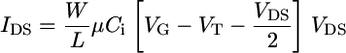 |
[1] |
 |
[2] |
Fig. 1.

Schematic representation of the components of an OTFT showing the molecular structures of various organic semiconductors (Left) and self-assembled nanodielectrics I-III (Right). Highly n-type doped Si (100) wafers with a 1.5-nm native oxide or smooth ITO (a transparent conductor) were used as substrate/gate electrodes. Nanodielectric layers then were sequentially deposited from solutions of silane precursors Alk, Stb, or Cap. The OTFT device was completed by vacuum-deposition of 50-nm-thick layers of p- or n-type organic semiconductors 1-4 or solution-deposition of semiconductor 5, followed by source-drain gold electrode (100 nm) vacuum deposition.
Note that for a given device geometry and semiconductor, equivalent Ion:Ioff ratios are achieved at lower operating biases by increasing Ci, which stabilizes the carrier density in the semiconductor channel. This Ci effect on IDS is important for OTFTs considering the modest μ values of organic semiconductors, which are typically <1 cm2·V-1·s-1 vs. 103 cm2·V-1·s-1 for crystalline Si. Furthermore, high-quality ultrathin gate dielectrics will be essential in combination with small channel lengths for high frequency operation (11, 12) and self-assembled molecular electronics (refs. 13 and 14 and references therein).
Recent efforts to increase Ci have striven either to increase k or to reduce d while managing the aforementioned challenges, by using either self-assembled monolayers (SAMs) of monofunctional (15) and phenoxy-terminated (16) hydrocarbon chains or relatively thick sputtered films of conventional metal oxides having greater k than SiO2, e.g., BaSrxTi1-xO3 (11), Ta2O5 (17), or TiO2 (18). Ultrathin polymeric dielectrics fabricated by means of polymerization of self-assembled initiators (19) on the gate dielectric or crosslinking of conventional polymers with suitable silane reagents (M.-H.Y., unpublished data) are also promising approaches. As dielectrics, the high defect densities and fragility of simple alkyl SAMs result in low device yields and modest OTFT response, although terminal phenoxy functionalization, which is thought to enhance SAM packing and prevent semiconductor molecule intercalation (16), significantly improves pentacene TFT performance. The modular synthetic approach reported here utilizes 3D-crosslinked dielectric multilayers grown from solution by means of self-limiting sequential chemisorptive deposition of the following σ-π building blocks (Fig. 1): (i) α,ω-difunctionalized hydrocarbon chains (Alk) that transversely crosslink, enabling precision stepwise layer build-up, increasing interchain packing, and reducing defects/pinholes; (ii) highly polarizable “push-pull” stilbazolium layers (Stb) self-assembled into oriented π-electron layers that should stabilize charge carriers in the semiconducting channel, including bound and free charges (20); and (iii) octachlorotrisiloxane capping layers (Cap) that enhance multilayer structural robustness by capping/planarizing with a crosslinked, glassy siloxane polymer. The resulting OTFTs function in the sub1V bias regime and exhibit very low leakage currents over large gate electrode areas, very large breakdown fields, and excellent device characteristics.
Materials and Methods
Materials and Self-Assembly Procedure. Semiconductors 1-5 and Stb were available in our laboratory (see Supporting Materials, which is published as supporting information on the PNAS web site). Alk and Cap were purchased from Gelest (Morrisville, PA). All Si wafers and tin-doped indium oxide (ITO) substrates were cleaned according to standard procedures (see Supporting Materials) and were dried at 110°C for 5 min. All self-assembly procedures were performed in an N2-filled glove bag. A scheme describing the self-assembly process is shown in Fig. 2.
Fig. 2.

Schematic of the self-assembly of nanodielectrics I-III. Conditions were as follows: 5 mM Alk in dry toluene at 0°C in N2 for 1 h (I), 34 mM Cap in dry pentane at RT in N2 for 25 min (II), or 10 mM Stb in dry tetrahydrofuran at 60°C in N2 for 15 min (III), followed by hydrolysis with acetone-H2O solution.
Device Fabrication. For OTFTs, semiconducting materials (1-4) were vacuum deposited at ≈2 × 10⁻⁶ torr (500 Å, 0.2 Å·s-1 1 torr = 133 Pa) while maintaining the substrate-nanodielectric temperature at 60°C. Films of 5 were deposited from a xylene solution (500 ppm) at 105°C. Gold electrodes for OTFT/metal-insulator-semiconductor (MIS)/metal-insulator-metal devices were vacuum-deposited through shadow masks at 3 × 10⁻⁶ to 4 × 10⁻⁶ torr (500-1000 Å, 0.5 Å·s-1).
Electrical Measurements. All OTFT measurements were carried out in air except for compound 3, which was measured in vacuum (8 × 10⁻⁵ torr) by using a Keithley 6430 Sub-Femtoamp Remote Source Meter and a Keithley 2400 source meter, operated by a local labview program and general purpose interface bus communication. Triaxial and/or coaxial shielding was incorporated into Signatone (Gilroy, CA) probe stations to minimize the noise level. A digital capacitance meter (Model 3000, GLK Instruments, San Diego) and impedance/gain-phase analyzer (SI 1260, Solartron Analytical, Hampshire, U.K.) were used for capacitance measurements.
Results and Discussion
To validate the modularity of this approach and to elucidate structure-function relationships, three nanodielectrics of incrementally varied structure and thickness were fabricated (Figs. 1 and 2). These nanodielectrics are identified by the following nomenclature: I (layers, Alk+Cap), II (layers, Stb+Cap), and III (layers, Alk+Cap+Stb+Cap). The microstructures, electrical properties, and responses of TFTs fabricated with I-III were characterized as reported below. The synchrotron x-ray reflectivity-derived thicknesses of the nanoscopic dielectrics are 2.3 (I), 3.2 (II), and 5.5 (III) nm (±10%). Optical absorption (see Fig. 6, which is published as supporting information on the PNAS web site) and optical second-harmonic generation measurements on II and III demonstrate net polar alignment of the Stb dipoles with an average molecular tilt angle of ≈40° from the surface normal, whereas atomic force microscopy and SEM images of I-III are featureless, with rms roughness approximately that of the Si substrate, 0.5-1.0 nm, and consistent with crack/pinhole-free morphologies. The excellent insulating properties of I-III are demonstrated by cyclic voltammetry (Fig. 3a) by using ferrocene probe solutions with either bare ITO-coated glass working electrodes or those coated with I-III. From the magnitude of the current at any potential, it can be seen that there is passivation of the ITO surface with respect to ferrocene oxidation/reduction as successive ultrathin dielectric layers are built up, arguing that these multilayers eliminate the majority of pinholes (potential short circuits), which would compromise OTFT performance. This conclusion is further confirmed by quantitative solid-state leakage current measurements through the nanodielectrics, made on MIS and metal-insulator-metal (ITO-based; see Supporting Materials) sandwich structures fabricated by thermal evaporation of 200 × 200 μm2 Au contacts onto I-III (Fig. 3b). Although Si/Si native oxide substrates exhibit very large current densities of ≈0.1-1.0 A/cm2 at 1.0 V, thin films of I, II, and III reduce the leakage currents by ≈6 and ≈9 orders of magnitude, respectively. Current densities for III (≈10-9 A·cm-2) can be compared to reported SAM values spanning the broad range of 10-5 to 10-9 A·cm-2 for smaller area (100 × 100 μm2) Al contacts (21) to 100 to 10-5 A·cm-2 reported by others (15, 18, 19). The measured breakdown fields for I-III (5-7 MV·cm-1) rival or exceed those reported for far thicker (≈50 nm) metal oxide (17) and polymer (ref. 14 and references therein) dielectric layers (0.1-5 MV·cm-1), previously used in OTFTs.
Fig. 3.

Leakage current measurement for nanodielectrics I-III. (a) Film pinhole assay by cyclic voltammetry (current vs. voltage) by using ferrocene/ferrocenium+ solutions in tetrahydrofuran/tetrabutylammonium hexafluorophosphate (Ag pseudoreference electrode; Pt counter electrode) using bare ITO (dotted line) and nanodielectrics I-III coated ITO as working electrodes (solid line). Electrode areas are ≈0.5 cm2.(b) Measured leakage current density J vs. voltage plots without (bare substrate) and with nanodielectrics I-III in MIS sandwich structures on n+-Si. As expected, the J-V curves are slightly asymmetric at ≈0.0 V, reflecting the different nature of the Au-siloxane-insulator and n+-Si-native oxide-insulator interfaces.
Capacitance-voltage (C-V) measurements were carried out on MIS structures at 102 to 105 Hz (22-24) (Fig. 4). With n+-Si as the semiconductor, capacitance is expected (and found) to increase on sweeping the bias with respect to the metal contact from negative (depletion in the semiconductor) to positive (accumulation). Capacitance- and dielectric loss (tanδ)-frequency plots (Fig. 4b) reveal maximum capacitances Ci = 400 (I), Ci = 710 (II), and Ci = 390 (III) nF·cm-2 (±5%) at 102 Hz, with slight fall-off (≈15%) at higher frequencies. These values are far greater than the capacitance of conventional 300-nm-thick SiO2 dielectrics typically used for OTFTs (≈10 nF·cm-2), greater than our estimates for the best siloxane SAM (≈150 nF·cm-2) (24), and comparable to the highest reported for a metal oxide dielectric, Ci = 150-750 nF·cm-2 in far thicker (d = 50-100 nm) sputtered TiO2 films (17). The nanodielectric loss factor (≈10-1 to 10-2) is greater than in optimized complementary metal oxide semiconductor SiO2 dielectrics (≈10-4) and, at all frequencies, I-III exhibit 0.1-0.4 V hystereses. However, annealing at 120-180°C reduces all hystereses to <0.1 V and reduces frequency-dependent C-V dispersion, suggesting that pristine I-III contain some quantities of fixed positive charges (Qf), ≈ 2 × 10¹² to 5 × 1012 cm-2 (23, 24).† Interface state densities (Dit) calculated from standard C-V and G-V (conductance-voltage) plots (25) are ≈ 3 × 10¹² eV-1·cm-2 (1 eV = 1.602 × 10⁻¹⁹ J). Importantly, annealing reduces Qf and Dit to ≈1011 cm-2 and ≈1011 eV-1·cm-2, respectively, which are near standard values for SiO2 and many high-k dielectrics (22).
Fig. 4.

Capacitance/loss measurements for I-III in MIS structures for nanodielectrics I (red), II (blue), and III (black) of Fig. 1. (a) Measurement of nanodielectric capacitance-voltage electrical characteristics at 104 Hz (solid line is the forward scan; broken line is the return scan). (Inset) Equivalent circuit representation. Note that the contribution of the nanodielectric capacitor (C) component to the total circuit impedance predominates over the series (Rs) and parallel (Rp) resistances as well as over the estimated parasitic capacitance. (b) Frequency (f) dependence of the capacitance (solid lines) and loss (broken lines) in the accumulation regime (1 V) between 102 and 105 Hz for the indicated nanodielectrics.
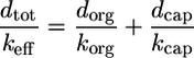
Also important are the magnitudes of the effective dielectric constants [keff = (Ci · dI-III)/ε0, Eq. 2] achieved in I-III, which are best estimated by measuring Ci in metal-insulator-metal structures (see Fig. 7, which is published as supporting information on the PNAS web site). Note that the presence of the Si-SiO2 interface strongly limits the maximum charge storage in the accumulation layer resulting in underestimated Ci values (24).‡ If the contributions of individual Alk and Stb organic layers (korg) are estimated by pragmatically assuming parallel-plate capacitors of thickness dI-III = dorg + dcap in series (Eq. 3)with Cap forming a SiOx network (dcap = 0.83 ± 0.1 nm by x-ray reflectivity) (26), then keff of I and II can be approximated by multilayers composed of Alk and Stb monolayers and oxide layer (kox ≈ 3.9) (10).
 |
[3] |
From the maximum metal-insulator-metal capacitance values [Ci = 1,100 (I), 2,500 (II), and 760 (III) nF·cm-2 (±5%)], korg of the Alk and Stb layers is estimated to be ≈2.5 (close to that of bulk paraffins and alkyl SAMs) (27) and ≈16, respectively. This result illustrates the strategic importance for this and future work of highly π-polarizable dipolar layers in enhancing keff, hence increasing Ci while preserving excellent insulator properties.
OTFTs (Fig. 1; L = 100 μm, W = 5 mm) were next fabricated on I-III, with all devices exhibiting reproducible I-V characteristics at low biases with classical linear and saturation response (10), as exemplified with typical p-type (1) and n-type (4) semiconductors (Fig. 5). Note that the operation window can be enlarged substantially by substituting multilayer III for II/I (Fig. 5b), because of the increased breakdown resistance, in agreement with the aforementioned leakage current data. Similar transistor characteristics are obtained for a range of vapor/solution-deposited organic semiconductors, demonstrating broad generality. In marked contrast, control devices fabricated with a thicker SiO2 dielectric require far larger operating voltages for useful IDS (Fig. 5a Inset).
Fig. 5.

Current-voltage performance characteristics as a function of gate voltage (VG; values indicated in vertical sequence in each plot) for nanodielectric-based organic transistor devices fabricated with the indicated organic semiconductors (molecular structure key in Fig. 1) on an n+-Si gate. (a) II/semiconductor 1; p-type. (Inset) SiO2 (300 nm)/semiconductor 1; p-type. (b) TFT transfer plot of current vs. gate voltage for III/semiconductor 1; p-type. (c) III/semiconductor 4; n-type. (d) OTFT fabricated on a transparent conducting ITO gate: III/semiconductor 1; p-type.
Nanodielectric III was next evaluated extensively in TFT geometries. Typical laboratory scale device fabrication yields were >98%. Table 1 summarizes data for semiconductors 1-5 (operating biases 0.0 to ±1.0 V) and for comparison, those using standard 300-nm SiO2 as the gate dielectric (operating biases 0 to ±100 V). Note that comparable μ values are now obtained at far smaller operating biases and that VTs are now only fractions of volts. The Ion:Ioff ratios should be further enhanced with second-generation device configurations and by more elaborate patterning of the semiconductor (28). Note also that TFTs fabricated on glass-coated ITO gates function comparably, demonstrating that a Si/Si native oxide gate is not required to achieve excellent performance (Fig. 5d and see also Fig. 8, which is published as supporting information on the PNAS web site) and that optically transparent low-voltage devices are readily fabricated. These nanodielectrics also can be used to fabricate flexible TFTs on commercially available plastic (Mylar)-coated ITO gates (see Fig. 9, which is published as supporting information on the PNAS web site), demonstrating applicability to transparent flexible plastic electronics. Finally, note that the thermal stability of the new nanodielectrics (Tdec > 200-300°C) suggests compatibility with inorganic semiconductors that can be deposited at such low temperatures.
Table 1. Field effect transistor data for organic semiconductors 1-5 using the nanodielectric III on n+-Si substrates.
| Semiconductor | μ, cm2·V-1·S-1 | Ion:Ioff* | VT, V |
|---|---|---|---|
| 1 | 0.06 (0.04) | 7 × 10² (104) | 0.08(−4) |
| III† | 0.03 | 6 × 10² | 0.05 |
| II | 0.02 | 1 × 10³ | 0.06 |
| I | 0.04 | 8 × 10² | 0.03 |
| 2 | 0.002 (0.02) | 5 × 10² (104) | −0.17 (2) |
| 3 | 0.02 (0.2) | 6 × 10² (105) | 0.21 (14) |
| 4 | 0.003 (0.001) | 3 × 10² (104) | −0.22 (20) |
| 5 | 0.01 (0.02) | 2 × 10² (104) | −0.20 (−40) |
Operating biases were 0.0 to ±1.0 V. Data in parentheses are for 300-nm-thick SiO2 dielectric devices. All TFT mobilities (μ) and threshold voltages (VT) are calculated in the saturation regime (11).
Calculated at VG = 0.0 to ±1.0 V (0 to ± 100 V) and VDS = ±1.0 V (± 100 V).
Data for nanodielectric III on glass-ITO substrates.
Conclusions
The aforementioned results demonstrate that designed self-assembling building blocks incorporating extensive 3D crosslinking and π-electron constituents enable precise, solution phase fabrication of extremely thin, nanostructurally ordered, pinhole-free, high-capacitance/high-k/low leakage organic multilayer dielectrics. These molecule-derived 2.3- to 5.5-nm-thick dielectrics can be efficiently integrated into large-area p- and n-channel OTFTs (single TFT area ≈ 1012 nm2) demonstrating great uniformity with a variety of substrates. The results argue that many of the charge transporting limitations of current organic semiconductors can be circumvented and that this assembly methodology combined with other crosslinkable high-k π-electron modules should be adaptable to creating even higher dielectric constant and higher capacitance molecular multilayers.
Supplementary Material
Acknowledgments
We thank Prof. P. Dutta and Dr. C. Yu for helpful discussions. This work was supported by the National Aeronautics and Space Administration Institute for Nanoelectronics and Computing, the Motorola Technology Center, the Office of Naval Research, and the National Science Foundation-Materials Research Science and Engineering Center program through the Northwestern Materials Research Center.
Author contributions: A.F. and T.J.M. designed research; M.-H.Y. and A.F. performed research; M.-H.Y. contributed new reagents/analytic tools; M.-H.Y., A.F., and T.J.M. analyzed data; and A.F. and T.J.M. wrote the paper.
Abbreviations: ITO, tin-doped indium oxide; SAM, self-assembled monolayer; MIS, metalinsulator-semiconductor; TFT, thin-film transistor; OTFT, organic TFT.
Footnotes
When the C-V transition from inversion to accumulation is sharp with small changes in the depletion C-V slope with frequency (no “stretch-out”), interface trap contributions are generally ignored (they cannot follow the ac voltage at high frequencies), and fixed charge density can be estimated from Qf = CΔVFB, where ΔVFB ≈ [VFB(105 Hz) - VFB(102 Hz)].
From published data (24), we estimate k < 1 (nonphysical) for a number of simple alkyl SAM grown on Si-native oxide substrates.
References
- 1.Kagan, C. R. & Andry, P., eds. (2003) Thin-Film Transistors (Marcel Dekker, New York), pp. 377-425.
- 2.Dimitrakopoulos, C. D. & Malenfant, P. R. L. (2002) Adv. Mater. 14, 99-117. [Google Scholar]
- 3.Sirringhaus, H. (2003) Nat. Mater. 2, 641-642. [DOI] [PubMed] [Google Scholar]
- 4.Ong, B. S., Wu, Y., Liu, P. & Gardner, S. (2004) J. Am. Chem. Soc. 126, 3378-3379. [DOI] [PubMed] [Google Scholar]
- 5.Katz, H. E., Lovinger, A. J., Johnson, J., Kloc, C., Slegrist, T., Li, W., Lin, Y.-Y. & Dodabalpur, A. (2000) Nature 404, 478-481. [DOI] [PubMed] [Google Scholar]
- 6.Facchetti, A., Yoon, M.-H., Stern, C. L., Katz, H. E. & Marks, T. J. (2003) Angew. Chem. Int. Ed. 42, 3900-3903. [DOI] [PubMed] [Google Scholar]
- 7.Sundar, V. S., Zaumseil, J., Podzorov, V., Menard, E., Willett, R. L., Someya, T., Gershenson, M. E. & Rogers, J. A. (2004) Science 303, 1644-1646. [DOI] [PubMed] [Google Scholar]
- 8.Stutzmann, N., Friend, R. H. & Sirringhaus, H. (2003) Science 299, 1881-1994. [DOI] [PubMed] [Google Scholar]
- 9.Crone, B., Dodabalapur, A., Lin, Y.-Y., Filas, R. W., Bao, Z., LaDuca, A., Sarpeshkar, R., Katz, H. E. & Li, W. (2000) Nature 403, 521-523. [DOI] [PubMed] [Google Scholar]
- 10.Sze, S. M. (1985) Semiconductor Devices: Physics and Technology (Wiley, New York), 2nd Ed.
- 11.Dimitrakopolous, C. D., Purushothaman, S., Kymissis, J., Callegari, A. & Shaw, J. M. (1999) Science 283, 822-824. [DOI] [PubMed] [Google Scholar]
- 12.Scheinert, S., Doll, T., Scherer, A., Paascj, G. & Hörselmann, I. (2004) Appl. Phys. Lett. 84, 4427-4429. [Google Scholar]
- 13.Kagan, C. R., Afzali, A., Martel, R., Gignac, L. M., Solomon, P. M., Schrott, A. G. & Ek, B. (2003) Nano. Lett. 3, 119-124. [Google Scholar]
- 14.Chua, L.-L., Ho, P. K. H., Sirringhaus, H. & Friend, R. H. (2004) Appl. Phys. Lett. 84, 3400-3402. [Google Scholar]
- 15.Collet, J., Tharaud, O., Chapoton, A. & Vuillaume, D. (2000) Appl. Phys. Lett. 76, 1941-1943. [Google Scholar]
- 16.Halik, M., Klauk, H., Zschieschang, U., Schmid, G., Dehm, C., Schuetz, M., Maisch, S., Effenberger, F., Brunnbauer, M. & Stellacci, F. (2004) Nature 431, 963-966. [DOI] [PubMed] [Google Scholar]
- 17.Tate, J., Rogers, J. A., Jones, C. D. W., Vyas, B., Murphy, D. W., Li, W., Bao, Z., Slusher, R. E., Dodabalapur, A. & Katz, H. E. (2000) Langmuir 16, 6054-6060. [Google Scholar]
- 18.Wang, G., Moses, D., Heeger, A. J., Zhang, H.-M., Narasimhan, M. & Demaray, R. E. (2004) J. Appl. Phys. 95, 316-322. [Google Scholar]
- 19.Rutenberg, I., Scherman, O. A., Grubbs, R. H., Jiang, W., Garfunkel, E. & Bao, Z. (2004) J. Am. Chem. Soc. 126, 4062-4063. [DOI] [PubMed] [Google Scholar]
- 20.Nalwa, H. S., ed. (2001) Handbook of Advanced Electronics and Photonic Materials and Devices (Academic, San Diego), Vol. 4, pp. 175-198. [Google Scholar]
- 21.Boulas, C., Davidovits, J. V., Rondelez, F. & Vuillaume, D. (1996) Phys. Rev. Lett. 76, 4797-4800. [DOI] [PubMed] [Google Scholar]
- 22.Nicollian, E. H. & Brews, J. R. (1982) MOS (Metal Oxide Semiconductor) Physics and Technology (Wiley, New York).
- 23.Evangelou, E. K., Wiemer, C., Fanciulli, M., Sethu, M. & Cranton, W. (2003) J. Appl. Phys. 94, 318-325. [Google Scholar]
- 24.Fontaine, P., Goguenheim, D., Deresmes, D., Vuillaume, D., Garet, M. & Rondelez, F. (1993) Appl. Phys. Lett. 62, 2256-2258. [Google Scholar]
- 25.Hill, W. A. & Coleman, C. C. (1980) Solid-State Electron 23, 987-993. [Google Scholar]
- 26.Malinsky, J. E., Veinot, J. G. C., Jabbour, G. E., Shaheen, S. E., Anderson, J. D., Lee, P., Richter, A. G., Burin, A. L., Ratner, M. A., Marks, T. J. et al. (2002) Chem. Mater. 14, 3054-3065. [Google Scholar]
- 27.Miramond, C. & Vuillaume, D. (2004) J. Appl. Phys. 96, 1529-1536. [Google Scholar]
- 28.Gelinck, G. H., Huitema, H. E., van Veenendaal, E., Cantatore, E., Schrijnemakers, L., van der Putten, J. B., Geuns, T. C., Beenhakkers, M., Giesbers, J. B., Huisman, B. H., et al. (2004) Nature Mater. 3, 106-110. [DOI] [PubMed] [Google Scholar]
Associated Data
This section collects any data citations, data availability statements, or supplementary materials included in this article.