Abstract
Additively manufactured (AM) metal components often exhibit fine dendritic microstructures and elemental segregation due to the initial rapid solidification and subsequent melting and cooling during the build process, which without homogenization would adversely affect materials performance. In this letter, we report in situ observation of the homogenization kinetics of an AM nickel-based superalloy using synchrotron small angle X-ray scattering. The identified kinetic time scale is in good agreement with thermodynamic diffusion simulation predictions using microstructural dimensions acquired by ex situ scanning electron microscopy. These findings could serve as a recipe for predicting, observing, and validating homogenization treatments in AM materials.
Additive manufacturing (AM) is a suite of emerging technologies that creates three-dimensional metal [1], polymer [2], or ceramic [3] objects directly from digital models through an additive process.
While the potential of metal-based AM has been clearly demonstrated [4, 5], significant challenges remain from the perspective of materials science and engineering. In particular, metal-based AM processes such as selective laser melting [6], direct metal laser sintering [7], and electron beam melting [1] often involve rapid heating and cooling of metal powders to and from material melting temperatures. Combined with the additive nature of the build processes, heterogeneous microstructure, residual stress distortion, and material inconsistency are difficult to avoid [8]. These characteristics adversely affect the materials performance. To fulfill the potential of AM, these challenges must be addressed.
To minimize such problems, post-build heat treatments of AM parts are necessary to create a homogenized microstructure with reproducible mechanical properties. While the ex situ effect of post-build heat treatment has been evaluated for AM materials [9–11], an in situ study that reveals the fundamentally important heat-treatment kinetics remains elusive. In this letter, we present a study that combines modeling prediction, in situ high-energy synchrotron X-ray scattering experiments, and ex situ microscopic characterization to elucidate the homogenization kinetics in AM-produced Inconel 625 (IN625). In particular, we introduce a novel in situ SAXS characterization scheme that follows the diffusion (homogenization) process of a fixed sample volume at elevated temperature, and we present a correlation-coefficient analysis that quantifies the homogenization kinetics and reveals the temporal evolution of the microstructures.
IN625 is a nickel-based superalloy primarily strengthened by the solid-solution hardening from niobium and molybdenum in a nickel-chromium matrix. IN625 features a combination of high yield strength, fatigue strength, and excellent oxidation, creep and corrosion resistance in aggressive environments. IN625 is widely used in the industries where complex shapes and consequent extensive machining are often required. Due to this reason, AM was recognized as an appealing option for fabricating IN625 components during the early stage of AM development.[9, 12] Improved understanding of the detailed microstructural changes during the post-build heat treatment not only provides opportunities to optimize the mechanical properties of AM IN625 components, but also sheds light on the more general behavior of AM alloy components.
Table 1 shows the manufacturer-certified chemical composition of the raw powder material used in this study. A sieve analysis showed that 98% of the powder particles have diameters < 80 μm. The as-built IN625 specimen was produced using an EOS M270 laser-sintering powder-bed fusion system (EOS GmbH, Munich, Germany) 1. The laser was operated at 195 W with a scanning speed of 800 mm/s and a hatch spacing of 100 μm. The test blocks were removed from the base plate by electro-discharge machining without a stress-relieving heat treatment. Specimens were cut and mechanically polished following standard metallographic procedure.[13]
Table 1.
Chemical compositions (mass fraction × 100) of the raw IN625 powder (from EOS [20]), and in the interdendritic and dendritic regions of the as-built sample, and after a 1 h, 1150 °C heat treatment.
| Ni | Cr | Mo | Nb | Fe | Ti | Al | Co | |
|---|---|---|---|---|---|---|---|---|
| IN625 Powder | 65.44 | 20.11 | 8.79 | 4.03 | 0.74 | 0.35 | 0.34 | 0.2 |
| As-builtInterdendritic regionsa | 65.75 ± 0.32 | 25.05 ± 0.08 | 5.36 ± 0.20 | 2.21 ± 0.10 | 0.38 ± 0.02 | 0.16 ± 0.02 | 0.33 ± 0.04 | 0.11 ± 0.02 |
| As-builtOn the dendritesa | 61.94 ± 1.38 | 24.18 ± 0.41 | 6.87 ± 0.47 | 4.41 ± 0.99 | 0.34 ± 0.03 | 0.20 ± 0.03 | 0.60 ± 0.14 | 0.09 ± 0.03 |
| 1150 °C, 1 hheat treatedb | 63.74 ± 0.02 | 21.10 ± 0.00 | 8.32 ± 0.02 | 4.00 ± 0.01 | 0.71 ± 0.00 | 0.36 ± 0.00 | 0.32 ± 0.00 | 0.21 ± 0.00 |
The optimal temperature for homogenization heat treatment was predicted using the CALPHAD-based Thermotech Ni7 [14] thermodynamic database and the NIST Ni-based atomic mobility database [15]. Diffusion simulations at 870 °C and 1150 °C were performed using the DICTRA software [16], which is a finite difference code that assumes local equilibrium at each grid point and then solves a flux balance equation at each grid point for each time step.
The microstructure and element spatial distributions of the as-built and homogenized samples were obtained using a JEOL S-7100F field-emission scanning electron microscope (SEM) and energy dispersion spectroscopy (EDS). The SEM specimens were oriented in the plane perpendicular to the base plate which allows microstructural information related to the dendrite centers, inter-dendritic regions, and intra-dendritic regions to be acquired. To investigate the homogenization kinetics, we performed in situ synchrotron small-angle X-ray scattering (SAXS) experiments using the ultra-small angle X-ray scattering instrument at the Advanced Photon Source, Argonne National Laboratory. [17, 18] The SAXS sample was treated following a two-step heat treatment. The first annealing step at 870°C for 1 h is the recommended stress-relieving heat treatment for IN625 [19]; the second anneal at 1150°C for 1 h is the homogenization treatment called for by thermodynamic modeling, as described later. More experimental details can be found in the Supplementary Materials.
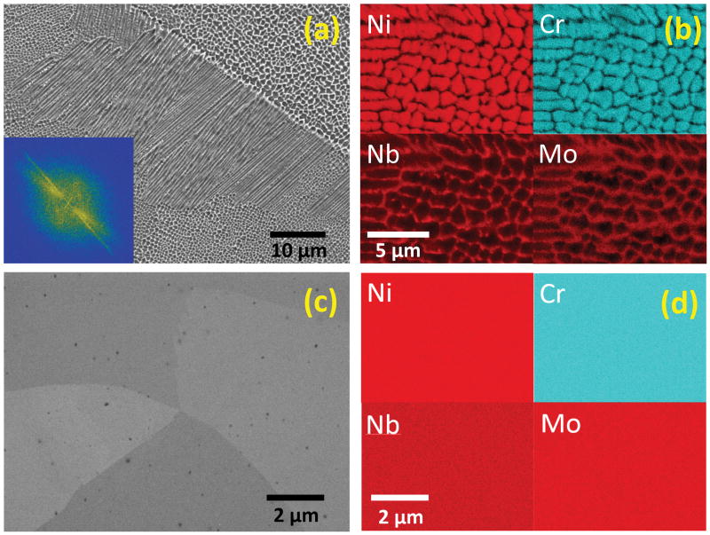
Figure 1(a) shows the representative microstructure of the as-built IN625 sample. It can be seen from Figure 1(a) that the cellular/dendritic microstructure manifests itself as both a columnar structure and an equiaxed cellular structure, depending on the angle between the solidification direction and the viewing plane. Both types of segregated domains have been extensively observed in and ubiquitously associated with AM metal components.[1, 20–23] These formations are closely tied to the rapid solidification inherent to the selective laser or electron beam melting involved in the AM process. It has been shown that when the melt pool solidifies, rapid cooling can occur via conduction into the substrate and the deposit, leading to directional growth of the columnar grains counter to the heat flux direction.[9] We found that the characteristic spacing is slightly different for the columnar dendrites (1 μm to 2 μm) and the cellular dendrites (2 μm to 3 μm), which may be attributed to the differences in the local cooling rates associated with the growth of these different microstructures. These dimensions are similar to those previously identified in AM Ni-based super alloys. [9, 20, 23–26]
Figure 1.
(a), (b) SE micrograph and elemental X-ray maps of as-built IN625 sample. Inset of (a) shows the Fourier transform of the imaged microstructure. (c), (d): SE micrograph and elemental X-ray maps of 1150°C, 1 h heat-treated sample.
Figure 1(b) shows the EDS elemental maps of Ni, Cr, Nb, and Mo within the same cellular regions of the as-built sample. We observe clear segregation of Nb and Mo to the interdendritic regions, and a corresponding deficiency of Ni and Cr. We note that the as-built SEM specimen was etched to enhance the details; hence the atomic mass fractions are not absolute. Still, detailed line scans show significant variations in the local atomic mass fractions. For example, Nb mass fraction varies from 1.95% to 5.15%, Mo 5.0% to 7.1%, Ni 61.1% to 67.1%, and Cr 23.6% to 25.4%. The EDS measurements had a spatial resolution of about 1 μm, so mass-fraction variations over shorter length scales are likely even more extreme. The statistically significant mass fractions of the elements above, as well as Fe, Al, Co, and Si on the dendrites and in the interdendritic regions are shown in Table 1, which demonstrates the compositional heterogeneity associated with the AM-induced microstructures. This behavior is consistent with previous findings in Ni-based super alloys, such as AM IN718Plus [25] and electron beam welded IN625. [24]
A common approach in industry is to optimize the mechanical properties of AM materials by post-build heat treatments, both to reduce AM-produced high residual stress and to produce a more homogeneous and consistent microstructure. For IN625, the recommended stress relieving condition for as-built AM IN625 is 1 h at 870°C. Following this treatment, we found that there was measurable formation of precipitates, but the coarse microstructure and elemental segregation remained nearly unchanged (data not shown).
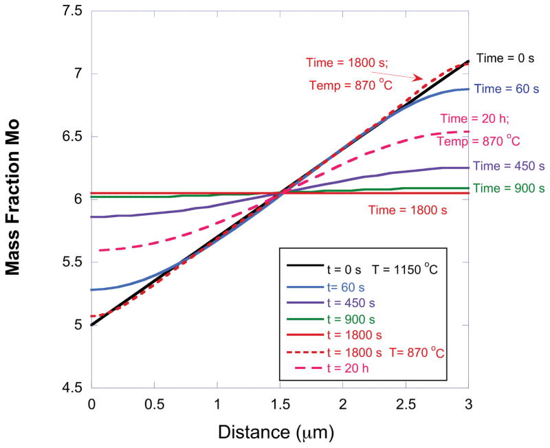
In our modeling effort to develop a heat treatment protocol for a homogenized microstructure with uniform mechanical properties, simulations were performed at 870 °C and 1150 °C using the DICTRA software assuming a dendrite size of 3 μm. The measured maximum and minimum compositions for Cr, Nb, and Mo were used for the initial linear composition profiles. The simulations were performed using a linear grid with 50 points. The goal of the simulations was to determine the amount of time needed to homogenize the observed composition gradients at the different temperatures. The simulations confirmed that Mo was the slowest diffuser, compared to Ni, Cr, and Nb. Figure 2 shows the predicted composition profiles for Mo at 870 °C and 1150 °C (The predicted composition profiles for other elements are shown in the Supplementary Material). The simulations predicted that after 900 s at 1150 °C, the microsegregation is homogenized, as seen in Figure 2. However, after 20 hours at 870 °C, the microsegregation is still present. These simulations provide a framework for optimizing the post heat treatment processes for as-built AM parts that require homogenization before service use.
Figure 2.
Predicted Mo composition profiles at 1150°C and 870°C.
To test the diffusion simulations, we chose 1150°C as the post-build heat treatment temperature for validation experiments, as it provides a balance between industrially practical annealing time and temperature.
SE micrographs for the 1 h, 1150°C homogenized sample are shown in Figure 1(c), where an equiaxed grain structure is clearly visible. EDS elemental maps of Ni, Cr, Nb, and Mo in Figure 1(d) demonstrate that compositional homogenization was achieved across the microstructure. The overall microstructure of the heat-treated sample is similar to previous observations in the wrought alloys and is in stark contrast to the results of similar experiments performed with a 1 h, 1050°C heat-treated AM sample, where microsegregation was still clearly present (data not shown). These observations suggest that the diffusion simulations could be used to predict the time that it takes to achieve homogenization in AM materials.
While the ex situ SEM measurement proves the effectiveness of the model-predicted homogenization heat treatment, it only demonstrates that homogenization is complete after 1 h. Also, while ex situ methods such as SEM and wavelength-dispersive spectroscopy have been used to characterize the homogenization process of alloys[27, 28], their success relies on randomly selected sample volumes being representative of the material under heat treatment. Such selection may be difficult to achieve for innately heterogeneous materials such as AM produced alloys. In situ SEM observation of the evolving sample microstructure at high temperature is possible, but this requires a highly specialized instrument, precise environmental control, and a sophisticated experimental setup.[29] An alternative approach is suggested by the inset of Figure 1(a), which shows a Fourier transform of the SE micrograph. This transform gives rise to a pronounced streaking pattern, which is directly related to the fine columnar dendritic structure. Such streaking patterns have also been identified in X-ray scattering experiments of various aligned fibular or layered structures. [30–32] Fundamentally, in the case of AM IN625, this streaking pattern can be associated with with the electron-density difference between that in the dendrites and that in the interdendritic regions. Qualitatively speaking, the length of the streaks is inversely proportional to the nominal width of the segregated features – the shorter the streak, the more diffuse the spatial electron-density distribution within the dendrites must be. In this sense, the streaking manifestation of the dendritic structure in reciprocal space may provide a valuable window to probe the statistically significant kinetics of the homogenization process. More details of the physical meaning of the streaking using a simple model can be found in the Supplementary Materials.
We further attempted to connect w, the “width” of the dendritic segregation layer in real space with the length of streaks, s, in reciprocal space, following w × s ≈ 2π. We found that the streaks in the as-built IN625 data have a nominal length in q on the scale of 0.1 Å-1, which translates to a segregated region width of ≈ 6 nm. This result is in good agreement with our CALPHAD-based solidification simulations on as-built AM IN625[33], which show that most of the elemental segregation occurs within several nm from the center of the interdendritic regions.
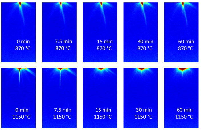
To interrogate the homogenization kinetics, we performed in situ synchrotron SAXS experiments on as-built IN625 specimens at two different heat-treatment temperatures: 870 °C and 1150 °C. The respective streaking patterns are shown in Figure 3. In these measurements, the contrast mechanism responsible for the streaks arises from differences in local electron density due to elemental segregation within the dendritic microstructure. At 870 °C, during the 1 h stress relief treatment, the streaking pattern remained largely unchanged, which suggests that the dendritic microstructure was stable. This agrees with the SEM observations outlined previously. Furthermore, at 1150 °C, there was a clear change in the streaking pattern as a function of time, with a rapid initial change and subsequent slower changes.We used a correlation coefficient analysis, a statistical approach increasingly identified as a powerful metric for evaluation of the degree of change hidden in time-series data, to extract quantitative details regarding the kinetics. [34–37] In our implementation, we defined the correlation coefficient C as , where A and B are two sets of image data of the same dimension, i and j refer to pixel indices, and A and B are the average pixel intensities on a normalized scale. We then calculated the correlation coefficients with respect to the first data set in each temperature series to show the degree of change.
Figure 3.
in situ SAXS streaking patterns of AM IN625 samples acquired at different time and temperatures. Top: 1 h at 870°C. Bottom: 1 h at 1150°C.
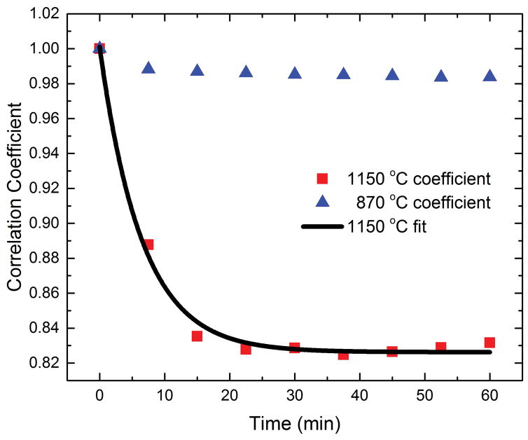
Figure 4 shows the calculated correlation coefficients for 870°C and 1150°C versus time. It is evident that at 870°C, the deviation of the correlation coefficient from one is small through the 1 h observation window, indicative of stable elemental segregation within the dendritic microstructure. This finding is consistent with the low atomic diffusion rate at this temperature. The small changes in the correlation coefficient are likely caused by the small amount of phase evolution mentioned above and slight changes in the microstructure resulting from stress relaxation.
Figure 4.
Temperature-dependent correlation coefficient between pairs of two-dimensional SAXS patterns as a function of time.
At 1150°C, the correlation coefficient analysis quantifies the homogenization kinetics. A simple exponential function C = C0 + A × exp(−λ0×t), where C is the correlation coefficient, t is time, and λ0 is the decay rate, describes the changes in the correlation coefficient. We found that the decay rate is (0.154 ± 0.012) min−1, which translates to a 95% completion of the kinetic process after ≈ 20 min. This value is consistent with the diffusion simulations that predicted a homogenized structure after 900 s (15 min). We note that perfect agreement is not expected since the experiments track the scattering contrast evolution caused by the elemental segregation while the model calculates the mean time for a single atomic species to diffuse a specific distance.
In conclusion, this study reports the first successful in situ characterization of the homogenization kinetics in AM IN625. We found that as-built AM IN625 exhibits a dendritic/cellular microstructure with distinctive compositional segregation. The industry-recommended stress-relieving heat treatment of 1 h at 870°C causes small changes in the phases present, but has no significant effect on the elemental segregation or dendritic microstructure. Starting from SEM images of the as-built microstructure, we performed diffusion simulations to predict that 1 h at 1150°C would be an effective homogenization temperature and time. The effectiveness of this heat treatment protocol was verified by ex situ SEM measurements. In addition, the model was further validated by a series of in situ synchrotron SAXS experiments at both temperatures, where we adapted a correlation coefficient analysis to quantify the kinetic phenomena associated with homogenization of the elemental segregation within the dendritic microstructure. While we cannot extrapolate the quantitative results to other AM materials, most qualitative findings here could potentially be generalized. In some ways, our approach offers a recipe for predicting, observing, and validating homogenization heat treatments in AM materials.
We note that the pervasiveness of the fine columnar dendritic microstructure is strongly tied to the growth of the primary dendrites associated with rapid solidification of individual melt pools produced by the fast-scanning electron or laser beam. The streaking pattern that we observed directly reflects the microscopic elemental segregation within this microstructure. Ultimately, with oversampling of the streaking patterns in reciprocal space, detailed electron density maps could be retrieved from coherent scattering patterns to offer an atomistic view of the microstructures. Such measurements are currently beyond our reach, but we have demonstrated that these streaking patterns already offer a realistic opportunity to quantify the changes in the dendritic structure under external influences such as temperature or tensile stress. This capability can contribute significantly to the goal of constructing processing-structure-performance maps for AM materials, and may be of importance to their eventual application in industries with high requirements for materials performance.
Supplementary Material
Acknowledgments
Use of the Advanced Photon Source, an Office of Science User Facility operated for the U.S. Department of Energy (DOE) Office of Science by Argonne National Laboratory, was supported by the U.S. DOE under Contract No. DE-AC02-06CH11357. The Engineering Laboratory at NIST built the IN625 samples used in this study.
Footnotes
Certain commercial equipment, instruments, software or materials are identified in this paper to foster understanding. Such identification does not imply recommendation or endorsement by the Department of Commerce or the National Institute of Standards and Technology, nor does it imply that the materials or equipment identified are necessarily the best available for the purpose.
References
- 1.Murr LE, Gaytan SM, Ramirez DA, Martinez E, Hernandez J, Amato KN, Shindo PW, Medina FR, Wicker RB. Journal of Materials Science & Technology. 2012;28:1–14. [Google Scholar]
- 2.Wendel B, Rietzel D, Kühnlein F, Feulner R, Hülder G, Schmachtenberg E. Macromol Mater Eng. 2008;293:799–809. [Google Scholar]
- 3.Travitzky N, Bonet A, Dermeik B, Fey T, Filbert-Demut I, Schlier L, Schlordt T. P Greil, Adv Eng Mater. 2014;16:729–754. [Google Scholar]
- 4.Gibson I, Rosen DW, Stucker B. Additive manufacturing technologies. Springer; 2010. [Google Scholar]
- 5.Kruth JP, Leu MC, Nakagawa T. CIRP Annals-Manufacturing Technology. 1998;47:525–540. [Google Scholar]
- 6.Kruth JP, Froyen L, Van Vaerenbergh J, Mercelis P, Rombouts M, Lauwers B. J Mater Process Technol J Mater Process Technol. 2004;149:616–622. [Google Scholar]
- 7.Agarwala M, Bourell D, Beaman J, Marcus H, Barlow J. Rapid Prototyping Journal. 1995;1:26–36. [Google Scholar]
- 8.White CW. Laser and electron beam processing of materials. Elsevier; 2012. [Google Scholar]
- 9.Dinda GP, Dasgupta AK, Mazumder J. Mater Sci Eng A. 2009;509:98–104. [Google Scholar]
- 10.Vrancken B, Thijs L, Kruth JP, Van Humbeeck J. J Alloys Compd. 2012;541:177–185. [Google Scholar]
- 11.Cheruvathur S, Lass EA, Campbell CE. JOM. 2016;68:930–942. doi: 10.1007/s11837-015-1754-4. [DOI] [PMC free article] [PubMed] [Google Scholar]
- 12.Paul CP, Ganesh P, Mishra SK, Bhargava P, Negi JA, Nath AK. Optics & Laser Technology. 2007;39:800–805. [Google Scholar]
- 13.Vander Voort GF. Metallography, principles and practice. ASM International; 1984. [Google Scholar]
- 14.Saunders N, Fahrmann M, Small CJ. In: Green KA, Pollock TM, Kissinger RD, editors. TMS; Warrendale, PA: p. 803. [Google Scholar]
- 15.Campbell CE, Boettinger WJ, Kattner UR. Acta Mater. 2002;50:775–792. [Google Scholar]
- 16.DICTRA. Thermo-Calc AB. Stockholm, Sweden: 2016. [Google Scholar]
- 17.Ilavsky J, Jemian PR, Allen AJ, Zhang F, Levine LE, Long GG. J Appl Crystallogr. 2009;42:469–479. [Google Scholar]
- 18.Ilavsky J, Zhang F, Allen AJ, Levine LE, Jemian PR, Long GG. Metallurgical and Materials Transactions A. 2013;44:68–76. [Google Scholar]
- 19.Babaye Khorasani F, Poling-Skutvik R, Krishnamoorti R, Conrad JC. Macromolecules. 2014;47:5328–5333. [Google Scholar]
- 20.Amato KN, Gaytan SM, Murr LE, Martinez E, Shindo PW, Hernandez J, Collins S, Medina F. Acta Mater. 2012;60:2229–2239. [Google Scholar]
- 21.Mumtaz KA, Erasenthiran P, Hopkinson N. J Mater Process Technol J Mater Process Technol. 2008;195:77–87. [Google Scholar]
- 22.Gu DD, Meiners W, Wissenbach K, Poprawe R. Int Mater Rev. 2012;57:133–164. [Google Scholar]
- 23.Jia Q, Gu D. J Alloys Compd. 2014;585:713–721. [Google Scholar]
- 24.Shakil M, Ahmad M, Tariq NH, Hasan BA, Akhter JI, Ahmed E, Mehmood M, Choudhry MA, Iqbal M. Vacuum. 2014;110:121–126. [Google Scholar]
- 25.Idell Y, Levine LE, Allen AJ, Zhang F, Campbell CE, Olson GB, Gong J, Snyder DR, Deutchman HZ. JOM. 2016;68:950–959. [Google Scholar]
- 26.Kirka MM, Unocic KA, Raghavan N, Medina F, Dehoff RR, Babu SS. JOM. 2016;68:1012–1020. [Google Scholar]
- 27.Semiatin S, Kramb R, Turner R, Zhang F, Antony M. Scr Mater. 2004;51:491–495. [Google Scholar]
- 28.Zhang W, Francesconi L, Evangelista E. Mater Sci Eng A. 1996;220:168–175. [Google Scholar]
- 29.Gregori G, Kleebe HJ, Siegelin F, Ziegler G. Journal of Electron Microscopy. 2002;51:347–352. doi: 10.1093/jmicro/51.6.347. [DOI] [PubMed] [Google Scholar]
- 30.McElhinny KM, Jacobberger RM, Zaug AJ, Arnold MS, Evans PG. Surf Sci. 2016 [Google Scholar]
- 31.Eymery J, Rieutord F, Favre-Nicolin V, Robach O, Niquet YM, Fröberg L, Mårtensson T, Samuelson L. Nano Lett. 2007;7:2596–2601. doi: 10.1021/nl070888q. [DOI] [PubMed] [Google Scholar]
- 32.Ran S, Fang D, Zong X, Hsiao BS, Chu B, Cunniff PM. Polymer. 2001;42:1601–1612. [Google Scholar]
- 33.Keller T, Lindwall G, Ghosh S, Ma L, Zhang F, Kattner UR, Lass EA, Idell Y, Williams ME, Guyer JE, Campbell CE, Levine LE. 2016 to be submitted to Acta Materialia. [Google Scholar]
- 34.Zhang F, Allen AJ, Levine LE, Ilavsky J, Long GG. Metall Mater Trans A. 2012;43:1445–1453. [Google Scholar]
- 35.Zhang F, Allen AJ, Levine LE, Ilavsky J, Long GG, Sandy AR. J Appl Crystallogr. 2011;44:200–212. [Google Scholar]
- 36.Aoun B, Yu C, Fan L, Chen Z, Amine K, Ren Y. J Power Sources. 2015;279:246–251. [Google Scholar]
- 37.Franke D, Jeffries CM, Svergun DI. Nat Methods. 2015;12:419–422. doi: 10.1038/nmeth.3358. [DOI] [PubMed] [Google Scholar]
Associated Data
This section collects any data citations, data availability statements, or supplementary materials included in this article.


