

Abstract
Conduction spectroscopy measures the current I through a nanosystem as a function of the voltage V between two electrodes. The differential conductance, dI/dV, has peaks that can be assigned to resonance conditions with different electronic levels of the system. Between these increments, the current has roughly constant plateaus. We discuss how measurements of the current vs. voltage can be used to perform Boolean operations and hence construct finite state logic machines and combinational circuits. The inputs to the device are the source–drain voltage, including its sign, and a gate voltage applied in a manner analogous to optical Stark spectroscopy. As simple examples, we describe a two-state set–reset machine (a machine whose output depends on the input and also on its present state) and a full adder circuit (a circuit that requires three inputs and provides two outputs).
Keywords: conduction spectroscopy, nanoelectronics, quantum dots, single electron transistors, molecular logic
Confined nanosystems have well separated, discrete electronic levels with energy spacings that reduce with increasing size of the system. It is therefore possible to prepare nanodevices where the electronic states of the system are resolvable by conductance spectroscopy, meaning that level spacings are of the order of weak DC fields. Conductance spectroscopy can be implemented in a regime of strong coupling between the system and the electrodes in which the electrons tunnel, one at a time, through the system, or for weaker coupling where electrons can accumulate on the system (1–13). The system itself can be a molecule where the confinement is due to the localized levels. For solids, the confining potential well can be induced by external fields and/or by the finite size of a colloidal particle to generate a quantum dot (QD). Although the details of the system do matter a great deal, for the purpose of this work we need only the observation that there can be one or more discrete levels that can be accessed by varying the electric potential across the device. We consider a three-terminal device so that one cannot only vary a source–drain voltage (Vsd) across the system, but one also can apply an electric field or gate voltage (Vg) in a perpendicular direction. In terms of its contacts, the device is a transistor, but because of the discrete nature of its levels, we will claim that we can do much more. Unlike a solid-state transistor, we will not talk of the Fermi level of the system but only about its discrete and resolvable levels. For the intended applications, it is convenient to operate in the intermediate coupling regime where the departure of electrons out of the system is sufficiently slow that one can perform level-filling spectroscopy, yet the coupling is strong enough that after a finite time interval the excess electrons will tunnel out.
There have been extensive discussions aimed at using confined quantum structures to implement quantum computing (14–25). Our purpose here is distinctly more modest. We do use the discrete level structure made possible by quantum confinement, but we only take advantage of the occupancy of the level and not of its quantum mechanical phase. Indeed, in this work we use the most elementary question: “Is the level occupied or is it not?” In other words, we use occupancy as a classical Boolean variable having the values 1 (for “yes”) or 0, and from this code, we construct both combinational circuits and also finite state logic machines.
By using a variety of nanosystems, such as lithographic QDs, colloidal QDs, C60, molecules, metallo-organic complexes, etc. (1–11, 26–31), the following common characteristic can be established: As a function of the applied voltage, and at sufficiently low temperature and for slow tunneling rates, it is possible to obtain a rather sharp answer to the following question: Is a given level occupied or not?
Overview of the Physical Considerations
The observed current–voltage characteristics of nanosystems can be reproduced by quantum mechanical computations (32–38) of the current, and the results shown in this work are all based on such computations for a two-level model Hamiltonian. It is, however, important to emphasize that the I–V curves for nanodevices have a “universal shape” because to lowest order, there is a simple and common physical picture as illustrated in Fig. 1. Charge flow is possible when a discrete electronic state lies energetically within the “Fermi window” spanned by the source and drain electrodes. (Strictly speaking, the charge flow is determined by the respective chemical potentials; see below.) The window is an energy window defined by the range of voltage that is equivalent to an excess population of the single electron states in one electrode over the other, as a function of energy. At very low temperatures, the window is of constant height, being unity or zero. Hence, the condition for current to flow is that the system has at least one level lying in energy between the source and drain potentials. In other words, the window function is rectangular, centered at the Fermi energy of the electrode, with a width that equals the applied eVsd, where e is the electron charge. As the temperature increases, the sharp cutoffs at the two edges of the window become increasingly rounded as thermal excitation moves some electrons from energies below the Fermi EF, to energies higher than EF. For our purpose, we need the edge of the window function to be as sharp as practical, and so we take it that the temperature can be made low enough that kT ≪ eVsd because what determines the sharpness of the reading of an empty vs. an occupied level of the system is whether the level is resonant with one or another side of the Fermi window. The high contrast ratios that are observed in practice (1, 7, 10–12, 39) demonstrate that the required lower temperatures are quite realistic.
Fig. 1.

The computed current vs. source–drain voltage and the physics that leads to the staircase I–V plot (Inset). The source–drain voltage determines the span (the Fermi window) between the uppermost occupied levels of the electrodes on the left and right. As Vsd increases, additional levels can come within the window, resulting in an increase in the current. The step in the current is when a level just becomes resonant with the electrode (Inset). The two states of the set–reset machine, as indicated, differ in one additional level (as shown it is the lowest empty orbital) being within the span of the voltage. In the level-filling regime, this difference corresponds to an extra electron on the system.
Charge flows when a confined level of the nanosystem is energetically within the Fermi window and does not flow when there is no level within the window. The position (strictly speaking, the chemical potential; see below) of the level with respect to the window can be tuned in two independent ways. One is by controlling the source–drain voltage, Vsd. This voltage determines the span of the window function. The other is by applying a gate voltage, Vg, to shift the energy of the levels of the system. Either way, charge suddenly is set to move when the level coincides with the edge of the window at EF + eVsd/2 (or at EF – eVsd/2), and charge will continue to flow as long as this level remains within the window. At low temperature, the window function is rectangular, so when the level energy is within the Fermi window the current is carried by a single level and is constant. A plot of the current vs. the energy of the level tracks, therefore, the plot of the Fermi window vs. Vsd. It follows that I vs. Vsd is a staircase function, as shown in Fig. 1, so that the differential conductance, dI/dVsd, is maximal at the energy resonance condition between the level and either of the two edges of the window, Elevel = EF ± eVsd/2. In the limit of the temperature going down toward zero, the differential conductance becomes a delta function of the source–drain voltage. In general, nanodevices have more than one level. Therefore, as Vsd increases, the window can span additional levels. Theory and computations show that each time an additional level enters the window, the current rises to a new plateau (see Fig. 1), and such staircases are seen experimentally.
The logic machines that we discuss are similar in spirit to our earlier discussions (40–42) where the inputs to the system were not electrical but optical. The similarity comes about because in the optical case, we change the state of the machine by adding one or more photons. Here, we change the state by adding a discrete number (one or more) of electrons. The other similarity is in the use of the value of the excitation energy as a variable. In the optical case, we represent different inputs by light of different wavelengths. Here, we use different voltages. In practical terms, electrical addressing is quite different, and it allows us to contemplate solid-state devices rather than the gas-phase systems that we discussed for optical excitation. Also, particularly for quantum wells confined by external fields (7), carbon nanotubes (9, 12, 39), and colloidal QDs (1, 2, 4, 8), the level structure is rich and it is possible to think of adding more than one or two electrons to the system.
The two plateaus in the current vs. voltage curve that are labeled in Fig. 1 are sufficient to specify a two-state logic machine. The increase in the current between these two is due to an additional level being within the Fermi window. In the weak coupling tunneling regime, the higher plateau means an additional electron on the device. This occupancy is analogous to the optical case where the molecule is excited (deexcited) by absorbing (emitting) a photon. We have used this scheme to build prototypical finite state logic machines (41, 43). We use the term finite state logic machines in its technical meaning (44): The logic operations performed by the machine are determined not only by the next input but also by the present state of the machine. This response endows the machine with memory, meaning that how it proceeds to change depends on the state it was left in from the previous operation. Below, we discuss a set–reset machine. Although a set–reset machine is an elementary example of a finite state device, it does exhibit the essential characteristic that the same input can induce a different output depending on the present state of the machine. Furthermore, it will be clear that for such devices that can accommodate more than one extra electron (or hole), the two-level set–reset machine can be easily generalized to a multistate case.
The set–reset machine operates by distinguishing the different plateaus in the I–V curve. In The Logical Plane, we describe logic circuits that require examination of the peaks of the conductance, σ ≡ dI/dV. This requirement is because such a peak corresponds to a resonance condition between the level and the edge of the occupied band of states of the (left or right) electrode. These peaks in the conductance spectra are the analogs of the resonance conditions of optical spectroscopy. As in the optical case the energy of a level can be (Stark) shifted by changing the voltage across the system. Because of the narrow gaps, the shifts can be significant (34, 45–49). For the gate voltage the differential shift, α ≡ dElevel/edVg, is determined by the ratio of Cg/C where Cg is the gate capacitance and C = Cg + Cs + Cd is the total capacitance of the three-terminal device (7).
For the set–reset machine, all that we need is the conductance at one value (can be zero) of the gate voltage. Then, in The Logical Plane, we describe schemes where we need the conductance at two different values of the gate voltage. To explain the principle, it is convenient to generalize the discussion of conduction spectroscopy by working in a plane where the two Cartesian coordinates are the source–drain voltage as abscissa and the gate voltage as ordinate. In this so-called logical plane, also called a conductance map, a plot of the differential conductance of a one-level system will look like two lines intersecting at the level energy, E1 as shown in Fig. 2 Left. Each line represents a finite (strictly speaking, very high) differential conductance, whereas off the line the differential conductance is very much smaller. Lines defined by high differential conductance have been experimentally observed (1, 7, 10–12, 39) for a variety of systems where representing the scale of differential conductance by color coding exhibits the very high contrast that is possible for such measurements.
Fig. 2.

The logic plane for a one-level (Left) and a two-level (Right) system. Regions of different numbers of electrons on the nanosystem can be reached by varying the gate potential, Vg, and the source–drain potential, Vsd. The level energy E1 is defined such that the gate voltage E1/eα brings the level of the system to coincide with the Fermi level of the electrodes. The lines are the curves of maximal differential conductance and occur when a level is resonant with the edge of the Fermi window (see Fig. 1). Solid lines, the lines with a positive slope, are the resonant condition for the right electrode (Eq. 4). Dashed lines are the resonant condition for the left electrode (Eq. 6).
Even for one discrete level, there are two lines in the Vsd – Vg plane because the line going up is for the level matching the edge of the Fermi window of the electrode on the right, and the line going down is the resonance condition at the left electrode. As drawn in Fig. 2 Left, the lines are straight, and the figure has an inversion symmetry about the energy of the unperturbed level. The plot of current vs. source–drain voltage has an inversion symmetry about the point Vsd = 0. This symmetry is often what is observed, but the result is not essential. First of all, the inversion symmetry requires that neither electrode be grounded so that inverting the sign of the source–drain potential inverts the relative heights of the occupied orbitals in the two electrodes (see Fig. 1 Inset). Next, the mirror symmetry of I about the Vsd axis depends on the barriers to electron transfer between the system and either of the two electrodes being similar. If the two barriers are different, then when we invert the sign of Vsd the shift of the edge of the window is no longer from 1/2to –1/2 but from η to 1 – η where 0 < η < 1 (7). Detailed examination (46, 48, 50) shows that the energy of the level also can shift with the source–drain voltage, which will also break the symmetry. All of these refinements of the basic description can be used to advantage because they allow a better control over the level. However, in this first attempt, we use only the regime in which the response of the system is linear in the applied source–drain voltage.
Fig. 2 Right shows the logic plane for a system with two levels. In The Adder, we show how such a plane (strictly speaking, two horizontal lines in these planes) are sufficient to define a full adder. We do so in two stages. First, we show how a measurement of |IdI/dVsd| is sufficient to define a half adder. Then, the direction of current flow, meaning that the measurement is of IdI/dVsd, defines a full adder.
The Set–Reset Machine
The set–reset machine uses two distinct charge states of the device, which we call the N–1 and the N electron states. We use the two charge states as the two possible states of the machine. There are many devices, based either on molecules or on quantum wells, that can accept or lose more than just one electron. So one can imagine many-state machines, but the principle will be the same. In this machine, the gate voltage is fixed, say at the value A. The only variable for the two-level set–reset machine is the value of Vsd. We use two values. One, d, is in the region of N–1 electrons, and the other, D, is in the region of N electrons (see Fig. 1). Logic state 0 is a point in the N–1 electron region, a point defined by the two voltages A and d. Logic state 1 is a point in the N electron region, a point defined by the two voltages A and D.
The operation of the machine is shown in Table 1 and Fig. 3. The operations in successive rows of the table correspond to successive columns of the figure. The input is the value of Vsd. The “set” input is assigned the value 1 when the source–drain voltage has the value D and is zero otherwise. The “reset” input has the value 1 when the source–drain voltage is d and is zero otherwise. To change the input, we reduce the voltage to zero and then raise it to the desired value as shown in Fig. 3. The entire time interval required to lower and increase the voltage is one cycle time of the machine. The states of the machine are its being in one of the two possible plateaus as indicated in Fig. 1. As shown, the next state of the machine is determined by both the input and by the present state and not by the input (nor by the present state) alone.
Table 1. The set—reset machine.
| Present state | Set input | Reset input | Name of action | Next state |
|---|---|---|---|---|
| 0 | 0 | 0 | No change | 0 |
| 0 | 1 | 0 | Set | 1 |
| 1 | 1 | 0 | Set | 1 |
| 1 | 0 | 0 | No change | 1 |
| 1 | 0 | 1 | Reset | 0 |
| 0 | 0 | 1 | Reset | 0 |
Fig. 3.

A set–reset machine. (Upper) The operation of a set–reset machine in physical time. Each logic cycle requires the finite time interval Δt. During that time the voltage is or is not ramped up or down to its new value. The state is read at the end of the interval. The order of operations is the same as in Table 1. (Lower) A logic circuit representation of the set–reset machine. S and R are the set and reset inputs, and Q is the state. The feedback loop informs the machine about the current state. The half-moon is the standard notation for the OR gate. The open dot negates the output so that each of the two gates shown is a NOR gate. The filled dot shows a connection.
Fig. 3 shows how the set, S(t), and the reset, R(t), inputs vary as a function of the physical time t. Note that the cycle of a machine is, on the physical timescale, a finite time interval. This characteristic is equally true for optically addressed machines (41) and also for transistor-based computer circuits (44). Referring to Fig. 3 and Table 1, if the state of the machine is 0 and in the next cycle the source–drain voltage is increased to the value D, the new state is 1. But if the state of the machine is 0 and in the next cycle the source–drain voltage is kept at the value d, the new state is 0, the same as before the application of the input. This result shows that the final state depends on the input. But now use either one of these two inputs when the state of the machine is 1. The results (Table 1) are the opposite of what they were. This response shows that the final state depends not only on the input but also on the state of the machine. For a set–reset machine, the (Boolean) condition that S(t)R(t) = 1 is not allowed (51), which is how the value of the source–drain voltage can code for both states. In terms of the logical plane discussed in The Adder, the robustness of the machine is due to the observation that during the set (or the reset) operations, the next state is 1 (or 0) whether the present state is 0 or anywhere else in the N–1 electron region or whether the present state is 1 or anywhere else in the N electron region.
The principle that the output depends not only on the input but also on the state of the machine is why for some time (e.g., ref. 43) we advocate that molecules can be used not merely as switches but as a platform for an entire logic machine.
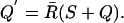
To write the operation of the two-state machine in Boolean notation we recall the identity  , where X and Y denote Boolean variables and the bar denotes the logical complement. Then the state of the machine in the next cycle, denoted Q′, is given by
 |
[1] |
By rewriting this equation as
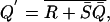 |
[2] |
we can exhibit a logic circuit built from feedback-coupled NOR gates (Fig. 3 Lower). To make the construction recall that a NOR gate whose input Boolean variables are X and Y has the output  . So a NOR gate has the output 0 unless both inputs have the value 0, when it has the value 1. The feedback coupling as shown in Fig. 3 ensures that the next state of the machine also depends on the present state and not only on the input.
The Logical Plane
We represent the state of the system as a point in the Vsd – Vg plane. The logical operations that constitute “the computation” will be represented by changes that we can induce in the location of the system point within the Vsd – Vg plane. Consider first a single quantum level, which, for convenience, we take to be the lowest empty level of our system. The zero of energy for the system is taken as a state with N–1 electrons. The chemical potential of the N electron system is
 |
[3] |
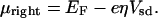
where α is the differential shift of the level due to the gate voltage, and we here take it to be constant, and E(N) is the energy of the unperturbed system. In the more general case where the level may be half-occupied, the effect of the charging energy is included in E(N). The chemical potential of the right electrode, which is depressed when the source–drain potential is positive (Fig. 1 Inset), is
 |
[4] |
In Fig. 2, we use the special case of symmetric barriers on the right and the left so that η = 1/2. The resonance condition for the right electrode, μright = μsystem(N), gives rise to the equation of the “bright” line in the Vsd – Vg plane, the line along which the differential conductance is maximal, which is
 |
[5] |
Now reverse the sign of the source–drain potential but keep the same value of the gate potential. Eq. 3 is unchanged, whereas in Eq. 4 the sign change means that the resonance condition is at the right electrode is not valid. But, if η = 1/2 we have that the left electrode is now resonant with the level of the system. If η ≠ 1/2, the left hand potential is
 |
[6] |
and so Eq. 5 reads for negative source–drain voltage but positive gate voltage,
 |
[7] |
The lines shown in Fig. 2 Right are the η = 1/2 case where the slopes are equal. To conclude, the resonance condition with the right electrode gives rise to the line with a positive slope. The line sloping down is the resonance condition for the left electrode. When the tunneling barriers are symmetric, the two slopes are equal in magnitude.
Next we enlarge the voltage range spanned by the gate so that we can include in the description another, higher-energy level, into which it is also possible to place an electron. One also can think of the higher energy as another electron in the previous level but being at a higher energy due to Coulomb repulsion. In this two-level system, each level gives rise to a pair of intersecting lines. The two sets of intersecting lines are shown in Fig. 2 Right.
Level filling spectroscopy of electric field confined QDs or of C60 or of colloidal QDs can place more than two electrons on the system, thereby giving rise to richer level structures than shown in Fig. 2. The building block is a pair of intersecting lines, and this motif is repeated at different heights along the ordinate (the gate voltage) at voltages corresponding to the addition of successive electrons to the systems. For our purpose, each level allows the computation of one Boolean function of two variables. So already two sets of intersecting lines, meaning a two-level structure, are sufficient to perform such operations as a binary addition where there are two outputs, the sum and the digit carried to the next addition.
The Adder
Our purpose is to design a sequential adder, namely a circuit that accepts as input two binary numbers and, if any, a carry digit from a previous addition. It provides as output the sum and a carry digit for the next addition. By the end of this logical cycle, it is ready to accept the next input. Our discussion breaks the operation of the adder into three stages. First it adds the two input numbers and provides intermediate values of the sum and a carry digit for the next addition. This logic operation is called a half adder. Then we take account of the carry bit from the previous addition to obtain the final value of the sum and of the carry bit to be used next. The third stage is to restore the system to a state where it is ready for the next cycle.
The operation of the half adder is shown in Fig. 4. There are four possible inputs (0,0; 1,0; 0,1; and 1,1), and these inputs are coded by representing the value of each binary number by either one or another value of voltage. So the four inputs are coded as four distinct points in the logical plane as shown in Fig. 4. The values of the source–drain and the gate voltages that are used are chosen such that each input is coded as a point that can be read with high contrast. The source–drain voltage D needs to be larger than d, but in practice it should not be so much larger that achieving the resonance condition brings the level too much down in energy. The gate voltage difference A – B needs to be equal to the excitation energy E2 – E1 (see Fig. 2 Right). Table 2 is a summary of the half adder action that makes use only of the right-hand side of the logic plane
Fig. 4.

Two views of the operation of a half adder. (Left) Measurement of the differential conductance at two values, A (Upper) and B (Lower), of the gate voltage, each one for two values of the source–drain voltage. These measurements provide four alternative points, which code for the four inputs of the binary adder. (Right) The four points shown in the logic plane. The half adder has two outputs, the sum and the carry digit. These outputs are provided by the following two Boolean questions: (i) Does level 1 satisfy a resonance condition? (Answer yes if you are along the lowest line on the right.) (ii) Does level 2 satisfy a resonance condition? (See Table 2.)
Table 2. The half adder.
| Input | Vg | Vsd | f(E1) | f(E2) |
|---|---|---|---|---|
| 0,0 | A | d | 0 | 0 |
| 0,1 | A | D | 1 | 0 |
| 1,0 | B | d | 1 | 0 |
| 1,1 | B | D | 0 | 1 |
The two Boolean functions [f(E1) and f(E2)] shown as output are the answers to the following questions. (i) Does level 1 satisfy a resonance condition? (ii) Does level 2 satisfy a resonance condition? They are seen to compute a XOR and an AND operation on the binary inputs that correspond to the intermediate values of the binary sum and the carry digit of this stage.
To operate as a full adder, we need to bring in the carry from the previous addition. We propose to do so by using the value of that digit, 0 or 1, to specify the sign of the source–drain voltage. This code is equivalent to specifying which half of the logical plane is to be used for the computation (Fig. 5). Thereby we have the truth table of a full adder, Table 3, with three inputs (two binary digits and a carry-in) and two outputs (a sum and the next carry that is to be the carry in for the next addition).
Fig. 5.

The full adder. It is the same as the half adder shown in Fig. 4 except that the sign of the voltage (sign of the current) also plays a role, meaning that we measure IdI/dV rather than |IdI/dV| of Fig. 4. There are three binary inputs (two numbers to be added and a carry bit from the previous addition), and these are coded by the eight points in the logical plane as shown. The four distinct outputs are shown in Table 3 and are coded by the following two questions. (i) Is level 1 resonant? (ii) Is level 2 resonant? The open and filled dots have opposite logical codes.
Table 3. The full adder.
| Input | Carry-in | Vg | Vsd | Sum | Carry-out |
|---|---|---|---|---|---|
| 0,0 | 0 | A | d | 0 | 0 |
| 0,1 | 0 | A | D | 1 | 0 |
| 1,0 | 0 | B | d | 1 | 0 |
| 1,1 | 0 | B | D | 0 | 1 |
| 0,0 | 1 | A | -d | 1 | 0 |
| 0,1 | 1 | A | -D | 0 | 1 |
| 1,0 | 1 | B | -d | 0 | 1 |
| 1,1 | 1 | B | -D | 1 | 1 |
A cycle of addition is now complete. Depending on the input, there can be an extra electron in level 1 or 2 or in both. To reset the machine, it is necessary to wait for the extra electron(s) to tunnel out.
Concluding Remarks
Recent progress in the understanding of the conduction of nanodevices (32–37, 52, 53) has led to the introduction of conduction spectroscopy of single nanoscale systems (QDs, molecules, etc.). Currently, this spectroscopy is being implemented both experimentally and theoretically. In certain ways, conduction spectroscopy is turning out already to be as rich in detail as optical electronic spectroscopy. This work requires only an elementary experimental observation: Have we or have we not achieved a resonance condition between the electrodes and the device? The two alternatives are taken to be two values of a Boolean variable. Thereby already a two-level system can implement logic well beyond a single switch. Much more can be done because most devices have a far richer level structure, and more than two levels can be accessed. In addition to performing Boolean operations, conduction spectroscopy, as does its venerable optical aunt, implies a response that depends not only on the input but also on the present state of the device. This feature allows the design of finite state logic machines.
Acknowledgments
We thank James Kinsey and Itamar Willner for their critical reading of a preliminary version. This work was supported by the U.S.–Israel Binational Science Foundation (Jerusalem) and by the European Community Specific Targeted Research Projects Future and Emerging Technologies Open Project MOLDYNLOGIC. F.R. is a Maître de Recherches, Fonds National de la Recherche Scientifique.
Author contributions: F.R., J.R.H., and R.D.L. performed research; and R.D.L. wrote the paper.
Abbreviation: QD, quantum dot.
References
- 1.Klein, D. L., Roth, R., Lim, A. K. L., Alivisatos, A. P. & McEuen, P. L. (1997) Nature 389, 699–701. [Google Scholar]
- 2.Porath, D., Levi, Y., Tarabiah, M. & Millo, O. (1997) Phys. Rev. B Condens. Matter 56, 9829–9833. [Google Scholar]
- 3.Alperson, B., Rubinstein, I., Hodes, G., Porath, D. & Millo, O. (1999) Appl. Phys. Lett. 75, 1751–1753. [Google Scholar]
- 4.Bakkers, E., Hens, Z., Zunger, A., Franceschetti, A., Kouwenhoven, L. P., Gurevich, L. & Vanmaekelbergh, D. (2001) Nano Lett. 1, 551–556. [Google Scholar]
- 5.Banin, U., Cao, Y. W., Katz, D. & Millo, O. (1999) Nature 400, 542–544. [Google Scholar]
- 6.Kouwenhoven, L. P. & McEuen, P. L. (1999) in Nanotechnology, ed. Timp, G. (Springer, New York), pp. 471–536.
- 7.Kouwenhoven, L. P., Austing, D. G. & Tarucha, S. (2001) Rep. Prog. Phys. 64, 701–736. [Google Scholar]
- 8.Millo, O., Katz, D., Cao, Y. W. & Banin, U. (2001) Phys. Rev. Lett. 86, 5751–5754. [DOI] [PubMed] [Google Scholar]
- 9.Liang, W., Bockrath, M. & Park, H. (2002) Phys. Rev. Lett. 88, 126801–126804. [DOI] [PubMed] [Google Scholar]
- 10.Luo, Y., Collier, C. P., Jeppesen, J. O., Nielsen, K. A., DeIonno, E., Ho, G., Perkins, J., Tseng, H.-R., Yamamoto, T., Stoddart, J. F. & Heath, J. R. (2002) ChemPhysChem 3, 519–525. [DOI] [PubMed] [Google Scholar]
- 11.Park, J., Pasupathy, A. N., Goldsmith, J. I., Chang, C., Yaish, Y., Petta, J. R., Rinkoski, M., Sthena, J. P., Abruna, H. D., McEuen, P. L. & Ralph, D. C. (2002) Nature 417, 722–725. [DOI] [PubMed] [Google Scholar]
- 12.Jarillo-Herrero, P., Sapmaz, S., Dekker, C., Kouwenhoven, L. P. & vanderZant, H. S. J. (2004) Nature 429, 389–392. [DOI] [PubMed] [Google Scholar]
- 13.Vanmaekelbergh, D. & Hens, Z. (2004) ChemPhysChem 5, 43–45. [DOI] [PubMed] [Google Scholar]
- 14.Deutsch, D. (1985) Proc. R. Soc. London A 400, 97–117. [Google Scholar]
- 15.Deutsch, D. (1989) Proc. R. Soc. London A 425, 73–90. [Google Scholar]
- 16.Kane, B. E. (1998) Nature 393, 133–137. [Google Scholar]
- 17.DiVincenzo, D. P. (1998) Proc. R. Soc. London A 454, 261–276. [Google Scholar]
- 18.Loss, D. & DiVincenzo, D. P. (1998) Phys. Rev. A 57, 120–126. [Google Scholar]
- 19.Cleve, R., Ekert, A., Macchiavello, C. & Mosca, M. (1998) Proc. R. Soc. London A 454, 339–354. [Google Scholar]
- 20.Nielsen, M. A. & Chuang, I. L. (2000) Quantum Computation and Quantum Information (Cambridge Univ. Press, Cambridge, U.K.).
- 21.DiVincenzo, D. P., Bacon, D., Kempe, J., Burkard, G. & Whaley, K. B. (2000) Nature 408, 339–342. [DOI] [PubMed] [Google Scholar]
- 22.Awschalom, D. D., Loss, D. & Samarth, N., eds. (2002) Semiconductor Spintronics and Quantum Computations (Springer, Berlin).
- 23.O'Brien, J. L., Pryde, G. J., White, A. G., Ralph, T. C. & Branning, D. (2003) Nature 426, 264–267. [DOI] [PubMed] [Google Scholar]
- 24.Mompart, J., Eckert, K., Ertmer, W., Birkl, G. & Lewenstein, M. (2003) Phys. Rev. Lett. 90, 147901–147904. [DOI] [PubMed] [Google Scholar]
- 25.Engel, H.-A., Golovach, V. N., Loss, D., Vandersypen, L. M. K., Elzerman, J. M., Hanson, R. & Kouwenhoven, L. P. (2004) Phys. Rev. Lett. 93, 106804. [DOI] [PubMed] [Google Scholar]
- 26.Liang, W., Shores, M. P., Long, J. L., Bockrath, M. & Park, H. (2002) Nature 417, 725–729. [DOI] [PubMed] [Google Scholar]
- 27.Banin, U. & Millo, O. (2003) Annu. Rev. Phys. Chem. 54, 465–492. [DOI] [PubMed] [Google Scholar]
- 28.Collier, C. P., Mattersteig, G., Wong, E. W., Luo, Y., Beverly, K., Sampaio, J., Raymo, F. M., Stoddart, J. F. & Heath, J. R. (2000) Science 289, 1172–1175. [DOI] [PubMed] [Google Scholar]
- 29.Collier, C. P., Wong, E. W., Belohradsk, M., Raymo, F. M., Stoddart, J. F., Kuekes, P. J., Williams, R. S. & Heath, J. R. (1999) Science 285, 391–394. [DOI] [PubMed] [Google Scholar]
- 30.Yu, H., Luo, Y., Beverly, K., Stoddart, J. F., Tseng, H.-R. & Heath, J. R. (2003) Angew. Chem. Int. Ed. 42, 5706–5711. [DOI] [PubMed] [Google Scholar]
- 31.Tseng, H.-R., Wu, D., Fang, N. X., Zhang, X. & Stoddart, J. F. (2004) ChemPhysChem 5, 111–116. [DOI] [PubMed] [Google Scholar]
- 32.Datta, S. (1995) Electronic Transport in Mesoscopic Systems (Cambridge Univ. Press, Cambridge, U.K.).
- 33.Imry, Y. (2002) Introduction to Mesoscopic Physics (Oxford Univ. Press, Oxford).
- 34.Xue, Y. Q., Datta, S. & Ratner, M. A. (2002) Chem. Phys. 281, 151–170. [Google Scholar]
- 35.Mujica, V., Kemp, M. & Ratner, M. A. (1994) J. Chem. Phys. 101, 6849–6855. [Google Scholar]
- 36.Yaliraki, S. N. & Ratner, M. A. (1998) J. Chem. Phys. 109, 5036–5043. [Google Scholar]
- 37.Nitzan, A. & Ratner, M. A. (2003) Science 300, 1384–1389. [DOI] [PubMed] [Google Scholar]
- 38.Remacle, F. & Levine, R. D. (2003) Isr. J. Chem. 42, 269–280. [Google Scholar]
- 39.Park, H., Park, J., Lim, A. K. L., Anderson, E. H., Alivisatos, A. P. & McEuen, P. L. (2000) Nature 407, 57–60. [DOI] [PubMed] [Google Scholar]
- 40.Remacle, F., Speiser, S. & Levine, R. D. (2001) J. Phys. Chem. A 105, 5589–5591. [Google Scholar]
- 41.Steinitz, D., Remacle, F. & Levine, R. D. (2002) ChemPhysChem. 3, 43–51. [DOI] [PubMed] [Google Scholar]
- 42.Remacle, F., Weinkauf, R., Steinitz, D., Kompa, K. L. & Levine, R. D. (2002) Chem. Phys. 281, 363–372. [Google Scholar]
- 43.Remacle, F. & Levine, R. D. (2001) J. Chem. Phys. 114, 10239–10246. [Google Scholar]
- 44.Kohavi, Z. (1999) Switching and Finite Automata Theory (Tata McGraw–Hill, New Delhi).
- 45.Remacle, F., Beverly, K. C., Heath, J. R. & Levine, R. D. (2003) J. Phys. Chem. B. 107, 13892–13901. [Google Scholar]
- 46.Remacle, F. & Levine, R. D. (2004) Appl. Phys. Lett. 85, 1725–1727. [Google Scholar]
- 47.Remacle, F., Willner, I. & Levine, R. D. (2004) J. Phys. Chem. B. 108, 18129–18134. [Google Scholar]
- 48.Basch, H. & Ratner, M. A. (2004) J. Chem. Phys. 120, 5761–5770. [DOI] [PubMed] [Google Scholar]
- 49.Ghosh, A. W., Rakshit, T. & Datta, S. (2004) Nano Lett. 4, 565–568. [Google Scholar]
- 50.Remacle, F. & Levine, R. D. (2004) Chem. Phys. Lett. 383, 537–543. [Google Scholar]
- 51.Nagle, H. T. J., Caroll, B. D. & Irwin, J. D. (1975) An Introduction to Computer Logic (Prentice–Hall, Englewood Cliffs, NJ).
- 52.Heath, J. R. & Ratner, M. A. (2003) Physics Today 56, 43–49. [Google Scholar]
- 53.Joachim, C. & Ratner, M. A. (2004) Nanotechnology 15, 1065–1075. [Google Scholar]