

Abstract
Electrochemistry is re‐gaining attention among scientists because the complex interplay between electronic and chemical interfacial processes lies at the bottom of a broad range of important research disciplines like alternative energy conversion or green catalysis and synthesis. While rapid progress has been made in recent years regarding novel technological applications, the community increasingly recognizes that the understanding of the molecular processes that govern macroscopic device properties is still rather limited – which hinders a systematic and more complete exploration of novel material and functionality space. Here, we discuss advanced Raman spectroscopies as valuable analysis tools for electrochemists. The chemical nature of a material and its interaction with the environment is contained in the label‐free vibrational fingerprint over a broad energy range so that organic species, solid‐state materials, and hybrids thereof can be investigated alike. For surface studies, the inherently small Raman scattering cross sections can be overcome with advanced nonlinear or nearfield‐based approaches that provide signal enhancements between three and seven orders of magnitude, sufficient to detect few scatterers in nano‐confined spaces or adsorbate (sub)monolayers. Our article highlights how advanced Raman techniques with extreme chemical, spatial and temporal resolution constitute valuable alternative surface analysis tools and provide otherwise inaccessible information about complex interfacial (electro)chemical processes.
Keywords: Raman spectroscopy, spectro-electrochemistry, surface spectroscopy, SERS/TERS
1. Setting the Scene for Raman Under Water
1.1. Nanoscale Chemical Characterization of Electrified Interfaces
When we ask an electrochemist about the most important and exciting part of the electrochemical system they investigate, they are likely to answer ”the electrochemical interface”. Independent of the electrochemical processes under study, ubiquitously ranging from electrocatalysis,1 to biological membrane behaviour,2 or energy conversion,3 to name a few key players, the central aspect common to all systems is the interface where the electrochemical action, namely, charge transfer and molecular conversion, takes place.
To tailor (electro)active interfaces for specific application needs, a fundamental understanding of the molecular processes that govern the macroscopic device behaviour is quintessential:4 What are the chemical species involved, where are they located, how do they respond to the local environment? The ideal electrochemist's tool should thus provide
high sensitivity to detect and characterize species at very low concentrations
chemical specificity to distinguish chemical species and their interaction with the environment, and
nanoscale chemical resolution to identify reactive species and sites,
all under realistic working conditions, i. e. at room temperature and in the presence of electrolyte.
Aside from the common electrochemist's workhorse, cyclic voltammetry, that provides a wealth of thermodynamic and kinetic information about interfacial properties and reactivity of electrodes ranging from mm to nm size,5 a number of advanced analytical tools are available to increase our knowledge about nanoscale electrochemical processes. Nanoscale topographic imaging can be achieved with electrochemical scanning probe approaches,6 even allowing video‐rate imaging of electrochemical processes,7 however, without chemical specificity. Scanning electrochemical microscopy6, 8 as well as scanning flow cell based tools9 provide complementary insight into (electro)chemical conversion processes with high temporal and spatial resolution. Nonetheless, as the detection sensitivity of scanning chemical analyses is mostly limited to the ppm range, individual reactive surface sites are difficult to characterize. In situ x‐ray scattering attracts increased attention among electrochemists to push chemical spatial resolution toward the molecular level.10 While important insight has been obtained into, for example, water adsorption on electrode surfaces,11 in situ x‐ray experiments remain rather scarce and expensive because they are synchrotron based.
Detailed information about adsorbate interactions can also be obtained with vibrational spectroscopy. For example, infrared spectroscopy and its nonlinear analogue sum frequency generation spectroscopy specifically tailored for electrochemical surface investigation provide direct chemical insight into molecular behaviour under reaction conditions with micronscale resolution.12, 13, 14, 15, 16 However, the accessible spectral range is typically limited on the low‐energy side, and aqueous electrolyte poses an additional difficulty because strong water absorption may mask vibrational bands of the reactive adsorbate species of interest.
Despite its inherent low scattering cross sections, Raman spectroscopy constitutes a valuable alternative for molecular‐scale surface analysis of electrochemical systems and processes.17, 18, 19 Advanced nonlinear and nearfield Raman tools are being developed to obtain in situ chemical fingerprints of physico‐chemical actions and reactions of molecules at complex electrified solid/liquid interfaces with ms temporal or sub‐ten‐nm spatial resolution. Examples presented in this review concentrate on energy and catalytic conversion processes as well as on the development of novel Raman‐based tools for nanoscale analysis, including the molecular behaviour in nanoporous systems studied with nonlinear Raman spectroscopy and the successful development and implementation of a novel tip‐enhanced Raman setup capable of working at solid/liquid interfaces of non‐transparent substrates under potential control. Correlating known macroscopic device behaviour to molecular‐level processes observed under in situ working conditions with advanced Raman approaches enables performance evaluation in an unprecedented detailed manner and paves the way for rational design of improved electrochemical systems.
1.2. Raman Spectroscopy Revisited
Vibrational Raman spectroscopy is based on the inelastic scattering of light where the energy difference between the incident and scattered photons (ωinc–ωsc; Raman shift) corresponds to the energy difference between two vibrational states of a material under investigation (Figure 1a). Excitation typically occurs from the ground state (ν0) into the first vibrational excited state (ν1) of the Raman‐active modes of a particular substance (Stokes scattering). A broad energy range is easily accessible with Raman spectroscopy, covering low‐energy modes between 50 and 300 cm−1, such as solid‐state phonons in metal oxides or metal‐organic vibrations, molecule vibrations between 700 and 2000 cm−1 and CH/OH stretches around 3000 cm−1 and higher.
Figure 1.

Top: a) Raman spectroscopy is based on the inelastic scattering of light from a sample. Molecules are excited from the vibrational ground‐state (ν0) to a vibrational excited state (ν1) whose energy difference matches the one between incident and scattered photons (ωinc–ωsc, Raman shift). Raman spectra cover a broad energy range, including solid‐state phonons or metal‐R interactions, the molecular fingerprint region, and high‐frequency modes of CH/OH. Bottom: To investigate a small amount of scatterers at interfaces or in confinement, the weak Raman scattering can be enhanced by nonlinear (coherent anti‐Stokes Raman, CARS) or nearfield (surface‐ or tip‐enhanced Raman, SERS/TERS) approaches. b) CARS is a four‐wave mixing technique where the enhancement is mainly based on coherent scattering from the sample. For c) SERS and d) TERS, field enhancement is achieved through the excitation of surface plasmons at rough surfaces or in a tip‐sample gap, respectively.
As vibrational energies depend on the atomic bonds involved, a Raman spectrum provides a unique chemical fingerprint of the sample. Furthermore, Raman spectroscopy provides direct quantitative information, because the scattering intensity is directly proportional to the number of scatterers. Note that Raman scattering cross sections are typically very low so that only about one in a million photons is inelastically scattered. As a result, Raman spectroscopy is conventionally employed to characterize bulk samples, such as powders or highly concentrated solutions, and second‐long spectral integration times and mW excitation powers are typically required to obtain good signal‐to‐noise spectra. On the one hand, this can be of advantage for electrochemical applications as working in aqueous electrolyte gives only weak, if any, Raman water signals. On the other hand, the investigation of (sub)monolayer adsorbates at electrochemical interfaces or in nano‐confinement is a huge challenge, because the sensitivity is generally too low to detect few scatterers. How can we exploit the advantages of Raman spectroscopy to access local information of the molecules at electrochemical interfaces?
2. Monitoring Molecular Interactions and Diffusion in Nanopores with Nonlinear Raman Spectroscopy
One way to enhance the inherently weak Raman scattering from confined molecules is to enforce coherent scattering with short, intense laser pulses. In coherent anti‐Stokes Raman spectroscopy (CARS), three photons of specified energies ω1,2,3 interact with the sample molecules in a way that a fourth photon at the anti‐Stokes energy is scattered (Figure 1b).
Through the coherent signal emission and nonlinear nature of the wave‐mixing approach, the CARS signal is enhanced by three to five orders of magnitude compared to conventional Raman scattering. For broadband CARS approaches covering a few hundred wavenumbers energy range, mathematical approaches to extract Raman‐like quantitative spectra from the CARS spectra are readily available.20, 21 As a result, spectral integration times can be reduced compared to conventional Raman spectroscopy to tens of ms, rendering CARS a valuable novel tool for in situ quantitative monitoring of dynamic molecular processes on the nanoscale. Commonly, CARS is employed in the field of bio(medical) imaging22, 23 and has only recently been introduced to the field of materials science. In the following, we highlight the potential CARS holds for the study of important (electro)chemical processes occurring inside nanopores, such as the catalytic chemical conversion on zeolite particles and the interaction and diffusion of water inside fuel‐cell membranes.
2.1. Zeolite Nanopore Catalytic Reactivity
Huge efforts are being carried out to develop ‘greener’ liquid‐phase, low‐temperature catalytic approaches, and molecular‐level insight into the spatio‐temporal distribution of reactants and products of catalytic conversion processes in situ would greatly benefit the development of cost‐efficient next‐generation catalysts. To answer fundamental questions about initial chemical transformation steps and the location of the corresponding catalytically active sites under liquid‐phase working conditions, new operando analytical approaches are sought.24, 25
Introducing CARS to the field of heterogeneous catalysis, the 3D distribution and geometric alignment of thiophene reactant in the nanopores of individual zeolite particles were mapped, giving unprecedented insight into the early activation stages of sulfur‐removing catalysis processes.27, 28 The full power of CARS for catalysis research was demonstrated by mapping renewable bio‐fuel conversion of glycol with alkenes on single catalyst particles with submicron 3D spatial chemical resolution. Figure 2a shows an overlay of the CAR band intensity of the reactant C=C double bond (red) and of the fluorescence intensity of the cations (green) in 2D maps recorded from an individual catalyst particle. After chemisorption of the alkene, reactant activation and formation of stabilized alkyl cations inside the zeolite pores can be watched to proceed with increasing reaction temperature from the rim toward the center of the zeolite, following the aluminum zoning naturally present in the catalyst. While conventionally, the ether product can only be detected off‐line after conversion, CAR spectra allow the in situ quantification of ether species directly on the catalyst: Figure 2b depicts CAR spectra recorded immediately after reaction onset (t=0 min) and after 90 min (t=90 min) and the respective non‐negative least squares fitting results. The yield of the ether product component (green) is seen to increase with time to about 50 %, about five times more than extracted from the catalyst after the reaction. In summary, the findings suggest that using small ZSM‐5 particles without aluminum zoning and finding more efficient ways to extract the product from the catalyst could greatly improve this important liquid‐phase catalytic reaction.
Figure 2.
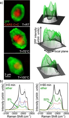
a) Combined CARS and 2‐photon fluorescence images of reactant (red) and product (green) distribution monitored in situ on a single zeolite particle as the reaction progresses with temperature. b) The ether product formation can be followed in situ in the time‐resolved CAR spectra with help of non‐negative least squares fitting. After 90 min, 50 % of the reactant has been converted into product. Reproduced from Ref.26
2.2. Water Transport in Nafion Fuel‐cell Membranes
Proper water management in fuel‐cell membranes is critical for the design of efficient devices, because the level of membrane humidity, specifically, the interactions between water molecules and membrane matrix, strongly affect the cell performance.29, 30 An in‐depth understanding of the water and proton transport inside the membrane nanopores is quintessential for the development of novel materials with increased proton transport efficiencies for improved fuel cells.
The nanoscale chemical interactions in two differently processed Nafion membranes, N117 and N212, of identical chemical composition but distinct proton transport properties has been elucidated with CARS.31, 32 While the Nafion signatures of both N117 and N212 are identical, distinct spectral shapes of the water OH stretch signature for the two membranes were observed (Figure 3a) that can be fitted with two types of water signatures (Figure 3b), namely bulk water (water molecules coordinated to other water molecules, blue) and under‐coordinated non‐bulk water (orange), located in the center of the ionic channels and at the interface between the hydrophobic channel walls and bulk water, respectively.31 The relative higher amount of non‐bulk water in N117 than in N212 can be explained by smaller nanopores in N117 that lead to more widely spaced SO3 − head groups, more surface area, and thus to more non‐bulk water compared to N212 (Figure 3c). The CARS results further suggest that non‐bulk water molecules diffuse an order of magnitude faster (Dnb≈16×10−10 m2/s) than bulk‐water molecules (Db≈10−10) inside the membrane nano‐channels, which could lie at the origin of the faster macroscopic water and proton transport observed in N117 compared to N212.31
Figure 3.

a) CAR spectra of hydrated N117 (green) and N212 (black) indicate chemical identity of the two Nafion membranes, but the presence of different water species. b) Fitting with bulk (blue) and non‐bulk (orange) water spectra show that N117 contains more non‐bulk water than N212 which can be explained by c) the different nanoscale chemical constitution of the membrane channels of N117 (smaller channels, less densely packed SO3 − groups) compared to N112. Reproduced from Ref.31
While CARS provides quantitative information about solid/liquid chemical interactions, molecular adsorption geometry and reactivity of nano‐confined species, it is important to remember that the coherent scattering response in fact still stems from the nanopore ensemble probed in the focal volume. As such, direct nanoscale sensitivity is still lacking with CARS. To obtain Raman responses from interfacial adsorbate monolayers, or even from individual scatterers, signal enhancement has to be achieved differently.
3. Hot‐spotting Nanoscale Chemistry with Surface‐enhanced Raman Spectroscopy
Surface‐enhanced Raman spectroscopy (SERS) is based on the formation of interface‐confined electromagnetic nearfields through plasmon excitation in nano‐structured coinage (Cu, Ag, Au) metal surfaces (Figure 1c). Raman signal enhancements of three to seven or more orders of magnitude are routinely achieved for molecules located in close vicinity of Au, Ag or Cu nanometer‐sized particles or structures or inside (sub‐)nanometer gaps, i. e. at ‘hot spots’ where the nearfield is particularly strong,33 rendering possible the trace analysis of small amounts of scatterers present in (sub)monolayer adsorbates, and even single‐molecule detection.34, 35 The potential of SERS characterization of electrochemical interfaces based on organic molecules adsorbed at metal surfaces has been repeatedly demonstrated.36, 37 In the following, examples for the specific strength of SERS regarding nanoscale chemical analysis of the electrosynthesis of novel metal‐organic hybrid materials and of the (photothermal) degradation of quantum‐dots (QDs) in sensitized solar cell devices are highlighted.
3.1. The Electrochemical Growth Mechanism of Cu‐MOF
Metal‐organic frameworks (MOFs) possess great potential for energy storage and conversion applications,38, 39 because their chemical and structural properties can be tuned through the intentional choice of metal ions and organic linkers. However, the lack of understanding of the nucleation stage and early growth process of this novel class of functional crystalline materials still hinders the development of tailored bottom‐up MOF fabrication protocols.
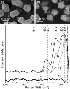
Specifically, electrochemical MOF synthesis offers extraordinary possibilities for precise size41, 42 and functionality43 tailoring through potential control. In a systematic SERS study of varying synthesis conditions, it was recently clarified that the electrochemical synthesis of prototype CuBTC proceeds in a two‐step oxidation mechanism at the Cu electrode surface.40 The strong nearfield signal enhancement at the atomically rough Cu electrode rendered possible the observation of the SERS signatures of the thin Cu2O precursor layer and of few CuBTC crystals forming on the electrode surface (Figure 4). Combined SEM and SERS results indicate that the common first reaction step is the oxidation of metallic Cu to Cu(I) oxide in the presence of H2O or O2. Cu2O is then further oxidized with the linker molecules to form Cu(II)BTC as octahedral crystals growing directly at the electrode surface. These findings generate interesting possibilities for the design of patterned MOF devices based on Cu2O pre‐patterning of any imaginable substrate.
Figure 4.

Scanning electron micrographs and SER spectra (insets) of CuBTC samples prepared under distinct electrochemical conditions: a) Cu/Cu oxide electrode, O2 presence, 1 V vs Cu/Cu+; b) Cu, oxide‐/O2‐free, 1 V vs Cu/Cu+; c) Cu/Cu oxide electrode, O2‐free, 1 V vs Cu/Cu+; d) Cu2O powder, O2 presence. Reproduced from Ref.40
3.2. The SERS Signature of PbS Quantum Dot Oxidation
PbS QDs, amongst other small‐bandgap semiconductor materials, are of prime interest for photovoltaic energy conversion, for example, in sensitized solar cells, reaching conversion efficiencies up to about 10 %.44 However, fast device degradation still hinders commercialization of QD‐sensitized solar cells. To understand the origin of device degradation, systematic analytical approaches to monitor the chemical state of the QD sensitizer in situ during fabrication and operation are needed.
SERS fingerprints of PbS QDs deposited on Au SERS substrates showed different stages of (photothermal) oxidative QD degradation.45 Isolated PbS QDs of 5 to 10 nm diameter were fabricated wet‐chemically on commercial nanostructured Au substrates following typical solar‐cell fabrication protocols under inert‐gas conditions in a glove box (Figure 5a, b). The SERS signatures from different sample batches indicate that the chemical state of the QD sensitizers strongly depends on the oxygen level in the preparation atmosphere as evident from the simultaneous relative decrease of PbS (196 cm−1) and increase of PbO (312 and 450 cm−1) Raman marker bands in the low‐wavenumber region (Figure 5c–e).45 Only samples prepared and tightly sealed–at lowest oxygen levels show long‐term stability even at increased power densities up to ca. 2×10¹⁸ W/m2. This work demonstrates how SER spectral markers allow the direct in situ visualization of the oxidative degradation state of PbS sensitizers, and SERS can serve as a fast benchtop control for in situ monitoring of PbS QD oxidation during device fabrication.
Figure 5.
Top: Scanning electron micrographs of a) bare and b) PbS QD‐covered Au substrate. Bottom: SER signatures of increasing PbS QD oxidation. c) Quasi‐intact PbS/Au, d) PbS/Au sealed in O2‐containing atmosphere, and e) unsealed PbS/Au samples measured in air. Reference spectrum of the bare Au substrate shown in f). Reproduced from Ref.45
These examples illustrate the great versatility of SERS for obtaining valuable in situ information about interfacial chemical conversion processes underlying photovoltaic applications or novel electrosynthesis approaches of advanced functional materials. The exact location and enhancement properties of the few active ‘hot spots’, however, still remains elusive, and the SERS response, in general, has to be considered an ensemble response from few scatterers in SERS‐active locations. To watch the first nucleation steps of single MOF crystals or probe size‐dependent optical properties of individual QDs, or even to record potential‐dependent maps of particle reactivity, it would be advantageous to create a free‐floating, movable ‘hot spot’ over a location of interest. In addition, such an external ‘hot spot’ would also broaden the applicability of SERS to oxide‐based or other non coinage‐metal electrodes.
4. (Electrified Solid/liquid Interfaces Probed with Tip‐enhanced Raman Spectroscopy
One way to generate a substrate‐independent ‘hot spot’ close to a sample interface is by means of tip‐enhanced Raman spectroscopy (TERS; Figure 1d), where a coinage‐metal scanning‐probe tip is brought in close vicinity to the surface and acts as a nano‐antenna to provide high field‐enhancement at the location of interest. With TERS, similar Raman signal enhancement as with SERS can be achieved to probe, for example, molecular catalytic properties46, 47 and interactions48 of a few scatterers underneath the tip at a chemical spatial resolution in the order of around 5 nm.49, 50
Due to the setup complexity, TERS experiments are commonly carried out in air. A few ultrahigh‐vacuum setups exist that provide particularly stable working conditions and extreme spatial51 or temporal resolution.52 However, air and vacuum are only crude approximations for electrochemical systems and there is a great interest in developing TERS systems capable of operating at electrified solid/liquid interfaces.
4.1. A Versatile Side‐illumination TERS for Solid/liquid Interfaces
The possibility to detect TER scattering at solid/liquid interfaces was first demonstrated by Zenobi and coworkers in 200953 with a transmission configuration. To enable the use of opaque electrodes, a side‐illumination configuration is desirable. Here, the main challenge lies in the beam aberrations that occur at the air/glass/water interfaces in the excitation laser path.54
Recently, we have developed a versatile side‐illumination solid/liquid TER spectroscope based on a home‐built sample cell design (Figure 6a) that can be easily implemented in a commercial scanning tunneling microscope (STM).55 By keeping the beam path in water a few mm short, focusing the laser onto the tip apex is as straightforward in water as in air.
Figure 6.

a) Side‐illumination TERS setup design for work at solid/liquid interfaces. b) Resonant TER spectra of malachite green isothiocyanate (MGITC) at Au (111) recorded in air (i) and in water (iii). Respective far‐field Raman spectra (ii, iv) and tip check (v). Nonresonant TER spectra of thiophenol at Au(111) in air (i) and in water (iii) and the respective far‐field spectra (ii, iv). Reproduced from Ref.55
As depicted in Figure 6b, a comparison of nearfield (i, iii) and farfield spectra (ii, iv) from electronically resonant dye molecules adsorbed on an opaque Au(111) crystal showed that similar Raman enhancement factors in the order of 105 can be reached for both in‐air (top; i, ii) and in‐water (middle; iii, iv) experiments. Importantly, the tip check (v) proved that the tip was clean and the TER spectra originated from dye molecules adsorbed at the single‐crystal substrate. Furthermore, the high surface sensitivity of the solid/liquid TER approach was confirmed by probing a monolayer of non‐resonant thiophenol/Au(111) (Figure 6c) where the in‐water experiment (bottom; iii, iv) shows a similar nearfield enhancement effect upon tip approach as the in‐air experiment (top; i, ii). The difference in relative Raman enhancement between air‐versus‐water dye and thiophenol experiments was ascribed to the difference in the chosen STM parameters for each experiment. Both, tip‐sample bias and tunneling current setpoint infl the tip‐sample distance. As the TER scattering intensity is known to depend exponentially on the tip‐sample gap size,50 a relative decrease in bias voltage and a relative increase in tunneling current setpoint lead to a smaller gap and hence to a TER intensity increase.56, 57, 58
4.2. Electrochemical TERS
Adjusting the solid/liquid TERS apparatus for potential‐dependent spectro‐electrochemical (EC‐TERS) experiments requires additional electrical contacting and control of the working electrode under investigation, thus rendering the setup even more complex and technically challenging. EC‐TERS has been a long sought‐after goal of the community, and finally in late 2015, the groups of Ren and of Van Duyne could first demonstrate its succesful implementation: Ren and coworkers observed potential‐dependent changes in TER spectra due to adsorbate reorientation on Au(111),59 followed shortly after by a report by the Van Duyne group who studied the redox behaviour of Nile Blue dye molecules with AFM‐based EC‐TERS.60 These works demonstrate the impressive potential that EC‐TERS holds for studying nanoscale electrochemical processes in molecular detail.
A few important points need to be considered for the successful implementation of EC‐TERS. First, as for all electrochemical experiments, utmost care has to be taken to provide a clean working environment. Note that this is of particular importance in TERS because of the extremely high chemical and spatial resolution. Even few contaminant molecules present in the ‘hot spot’ under the tip apex can significantly contribute to the TER signal. Next, particularly when working in an STM‐TERS configuration, the tip has to be insulated with a coating that prevents from Faradaic currents and does not fluoresce so as not to mask the TER signals with a strong background. We found that proper tip coating provides a much more stable ‘hot spot’ also under non‐electrochemical solid/liquid conditions.55
Furthermore, it is crucial that adsorption of probe molecules on the tip is prevented during the experiment, because the atomically rough tip surface itself can easily generate large SER signals that may be difficult to discriminate from the sample TER response. Bipotentiostatic control of substrate and tip can help to maintain the tip free from adsorbates; however, in STM‐based EC‐TERS, a rational choice of STM‐parameters has to be made to avoid molecular movement between sample and tip, and to keep the gap size stable.
Figure 7 shows potential‐dependent TER spectra of a monolayer of physisorbed adenine on Au(111) in 0.01 M H2SO4 from our laboratory (inset: cyclic voltammogram recorded in the EC‐TERS cell showing the reconstruction peak in the double‐layer region; scan rate 0.2 mV/s). With constant sample bias of 0.4 V, the characteristic adenine ring breathing (732 cm−1) and C=C/C=N stretching modes (1320 and 1460 cm−1) are observed at negative electrode potentials (−0.4 V vs Pt). When increasing the Au‐electrode potential to 0.2 V vs Pt, the adenine TER signatures decrease while the broad spectral background remains largely unchanged, indicating that the molecules stay adsorbed at the surface and the enhancement is still active. This trend of increasing band intensity with decreasing electrode potential agrees well with recently published electrochemical surface‐and shell‐isolated particle enhanced Raman spectroscopy data.61, 62 Note that the spectral changes are reversible, i. e. when applying a negative potential again, the adenine EC‐TER bands reappear.
Figure 7.
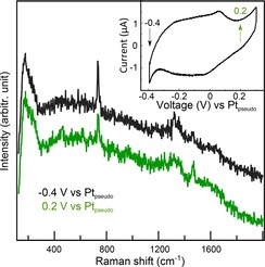
Potential‐dependent EC‐TER spectra of adenine at Au(111) showing a clear drop in band intensity of the 732 cm−1 ring breathing mode of adenine with increasing potential. The spectra are y‐offset for clarity. Inset: cyclic voltammogram recorded in the EC‐TERS cell with indicated measurement potentials.
The observed EC‐TER signature of adenine/Au(111) can be ascribed to potential‐induced molecular reorientation. The geometrical arrangement of adenine on Au single crystals has been extensively investigated with electrochemical infrared spectroscopy, EC‐STM and cyclic voltammetry.63, 64 There is a general agreement that in acidic media and at low adenine concentrations, as the case for the EC‐TERS data presented here, protonated adenine is chemisorbed at positive potentials, while at lower potentials, protonated adenine physisorbs. However the specific geometrical arrangement of the adenine molecules with respect to the electrode surface has remained controversial63 As the Raman polarizability tensor of the ring breathing mode (732 cm−1) is highly anisotropic,65, 66 a reorientation of the adenine rings could lead to the observed TER intensity changes. While the preliminary results shown here are very promising for future applications of EC‐TERS to the investigation of molecular behaviour at electrochemical interfaces, a more detailed interpretation of the EC‐TERS data at hand – but also in general – will require further experimental and particularly also simulation efforts to deconvolute the effects of the metal electrode, electrolyte, molecular interactions, surface charge and tip on the signal.
5. Summary and Outlook
We have presented examples of how advanced nonlinear or nearfield Raman spectroscopies can greatly benefit the nanoscale analysis of molecules or nanoparticles adsorbed at electrochemical interfaces or in confinement. As summarized in Table 1, each Raman‐based approach has its specific strengths and can be chosen based on the requirements of the system under investigation. Dynamic measurements of adsorbates inside nanoporous systems can be realized with nonlinear CARS, while solid/liquid TERS provides extreme chemical spatial resolution in the order of a few nm and precise interrogation of the sample region of interest. Both TERS and SERS can be operated under electrode potential control and thus are powerful spectro‐electrochemical tools for the visualization of potential‐dependent adsorbate reorientation or chemical conversion.
Table 1.
Comparison of the capabilities of conventional and enhanced Raman spectroscopies.
| Raman | CARS | SERS | TERS | |
|---|---|---|---|---|
| chemical specificity | ✓ | ✓ | ✓ | ✓ |
| single‐molecule sensitivity | X | X | ✓ | ✓ |
| intrinsic sectioning capability | X | ✓ | X | X |
| surface sensitivity | X | X | ✓ | ✓ |
| substrate‐independent enhancement | X | ✓ | X | ✓ |
| ms spectral integration time | X | ✓ | X | X |
| <10 nm lateral resolution | X | X | X | ✓ |
As an outlook, the development of an EC‐CARS approach could be expected to hold interesting opportunities for electrochemists: By adding an electrical contact to a membrane or catalyst as a working electrode, one could monitor potential‐controlled chemical processes inside nanoporous systems. 3D EC‐CARS imaging could reveal spatial heterogeneities in the potential‐triggered reactivity of functional membrane or catalyst materials. From a fundamental knowledge point of view, such experiments could greatly contribute to our understanding of the concepts of the electrochemical interface, double layer formation and local potential distribution inside electroactive nanopores.
Conflict of interest
The authors declare no conflict of interest.
Biographical Information
Natalia Martín Sabanés graduated in physics from Autonoma University of Madrid in 2011 and then enrolled in a Master program in biomedical physics at Complutense University in Madrid where she developed advanced analysis tools for NMR spectroscopy with Prof. Ruiz‐Cabello Osuna at CNIC. Currently, Natalia is working on her PhD with Dr. Domke at the Max Planck Institute for Polymer Research in Mainz where she is in charge of the development of electrochemical tip‐enhanced Raman spectroscopy.

Biographical Information
Dr. Katrin F. Domke studied chemistry at the Universities of Bonn, Alicante and CSIC/Sevilla and received her PhD in 2006 from the Free University Berlin/Fritz Haber Institute of the Max Planck Society for her seminal TERS work. After postdoctoral studies as a Feodor Lynen Fellow at Bern University and FOM Institute AMOLF in Amsterdam, in 2012 she set up an independent Emmy Noether Group at the Max Planck Institute for Polymer Research in Mainz. Katrin's research interests evolve around advanced molecular spectroscopy of electrified solid/liquid interfaces important for energy and catalytic conversion processes.

Acknowledgements
KFD gratefully acknowledges generous project funding through the Emmy Noether Program of the Deutsche Forschungsgemeinschaft (DO 1691/1‐1) and Marie Curie Actions of the 7th EU Framework Program (ITN‐FINON 607842).
N. Martín Sabanés, K. F. Domke, ChemElectroChem 2017, 4, 1814.
References
- 1. Koper M. T. M., Bouwman E., Angew. Chem. Int. Ed. 2010, 49, 3723–3725. [DOI] [PubMed] [Google Scholar]
- 2. Cheng C., McGonigal P. R., Stoddart J. F., Astumian R. D., ACS Nano 2015, 9, 8672–8688. [DOI] [PubMed] [Google Scholar]
- 3. Simon P., Gogotsi Y., Dunn B., Science 2014, 343, 1208–1210. [DOI] [PubMed] [Google Scholar]
- 4. Penner R. M., Gogotsi Y., ACS Nano 2016, 10, 3875–3876. [DOI] [PubMed] [Google Scholar]
- 5. Bard A. J., Murray R. W., P. Natl Acad. Sci. 2012, 109, 11484–11486. [DOI] [PMC free article] [PubMed] [Google Scholar]
- 6. Szunerits S., Pust S. E., Wittstock G., Anal. Bioanal. Chem. 2007, 389, 1103–1120. [DOI] [PubMed] [Google Scholar]
- 7. Wen R., Rahn B., Magnussen O. M., Angew. Chem. Int. Ed. 2015, 54, 6062–6066. [DOI] [PubMed] [Google Scholar]
- 8. Sun T., Yu Y., Zacher B. J., Mirkin M. V., Angew. Chem. Int. Ed. 2014, 53, 14120–4123. [DOI] [PubMed] [Google Scholar]
- 9. Grote J.-P., Zeradjanin A. R., Cherevko S., Mayrhofer K. J. J., Rev. Sci. Instrum. 2014, 85, 104101–5. [DOI] [PubMed] [Google Scholar]
- 10. Wu C. H., Weatherup R. S., Salmeron M. B., Phys. Chem. Chem. Phys. 2015, 17, 30229–30239. [DOI] [PubMed] [Google Scholar]
- 11. Velasco-Velez J.-J., Wu C. H., Pascal T. A., Wan L. F., Guo J., Prendergast D., Salmeron M., Science 2014, 346, 831–834. [DOI] [PubMed] [Google Scholar]
- 12. Osawa M., B. Chem. Soc. Jpn 1997, 70, 2861–2880. [Google Scholar]
- 13. Miranda P. B., Shen Y. R., J. Phys. Chem. B 1999, 103, 3292–3307. [Google Scholar]
- 14. Vidal F., Tadjeddine A., Rep. Prog. Phys. 2005, 68, 1095–1127. [Google Scholar]
- 15. Baldelli S., Acc. Chem. Res. 2008, 41, 421–431. [DOI] [PubMed] [Google Scholar]
- 16. Li J.-T., Zhou Z. Y., Broadwell I., Sun S.-G., Acc. Chem. Res. 2012, 45, 485–494. [DOI] [PubMed] [Google Scholar]
- 17. Fleischmann M., Hendra P., McQuillan A., J. Chem. Soc. Chem. Comm. 1973, 3, 80–81. [Google Scholar]
- 18. Jeanmaire D. L., Van Duyne R. P., J. Electroanal. Chem. 1977, 84, 1–20. [Google Scholar]
- 19. Tian Z.-Q., Ren B., Ann. Rev. Phys. Chem. 2004, 55, 197–229. [DOI] [PubMed] [Google Scholar]
- 20. Liu Y., Lee Y. J., Cicerone M. T., Opt. Lett. 2009, 34, 1363–3. [DOI] [PMC free article] [PubMed] [Google Scholar]
- 21. Day J., Domke K., Rago G., Kano H., J. Phys. Chem. B 2011, 115, 7713–7725. [DOI] [PubMed] [Google Scholar]
- 22. Kano H., Segawa H., Okuno M., Leproux P., Couderc V., J. Raman Spectrosc. 2015, 47, 116–123. [Google Scholar]
- 23. Winterhalder M. J., Zumbusch A., Adv. Drug Deliver. Rev. 2015, 89, 135–144. [DOI] [PubMed] [Google Scholar]
- 24. Roeffaers M. B. J., Sels B. F., Uji-I H., De Schryver F. C., Jacobs P. A., De Vos D. E., Hofkens J., Nature 2006, 439, 572–575. [DOI] [PubMed] [Google Scholar]
- 25. Weckhuysen B. M., Nat. Sci. Rev. 2015, 2, 147–149. [Google Scholar]
- 26. Domke K. F., Riemer T. A., Rago G., Parvulescu A. N., Bruijnincx P. C. A., Enejder A., Weckhuysen B. M., Bonn M., J. Am. Chem. Soc. 2012, 134, 1124–1129. [DOI] [PubMed] [Google Scholar]
- 27. Kox M. H. F., Domke K. F., Day J. P. R., Rago G., Stavitski E., Bonn M., Weckhuysen B. M., Angew. Chem. Int. Ed. 2009, 48, 8990–8994. [DOI] [PubMed] [Google Scholar]
- 28. Domke K. F., Day J. P. R., Rago G., Riemer T. A., Kox M. H. F., Weckhuysen B. M., Bonn M., Angew. Chem. Int. Ed. 2011, 51, 1343–1347. [DOI] [PubMed] [Google Scholar]
- 29. Hickner M. A., Pivovar B. S., Fuel Cells 2005, 5, 213–229. [Google Scholar]
- 30. Tsushima S., Hirai S., Prog. Energ. Combust. 2011, 37, 204–220. [Google Scholar]
- 31. Ling X., Bonn M., Parekh S. H., Domke K. F., Angew. Chem. Int. Ed. 2016, 128, 4079–4083. [Google Scholar]
- 32. Farrukh A., Ashraf F., Kaltbeitzel A., Ling X., Wagner M., Duran H., Ghaffar A., ur Rehman H., Parekh S. H., Domke K. F., Yameen B., Polym. Chem. 2015, 6, 5782–5789. [Google Scholar]
- 33. Otto A., J. Raman Spectrosc. 2006, 37, 937–947. [Google Scholar]
- 34. Kneipp J., Kneipp H., Kneipp K., Chem. Soc. Rev. 2008, 37, 1052–9. [DOI] [PubMed] [Google Scholar]
- 35. Stiles P. L., Dieringer J. A., Shah N. C., Van Duyne R. P., Ann. Rev. Anal. Chem. 2008, 1, 601–626. [DOI] [PubMed] [Google Scholar]
- 36. Wu D.-Y., Li J.-F., Ren B., Tian Z.-Q., Chem. Soc. Rev. 2008, 37, 1025–17. [DOI] [PubMed] [Google Scholar]
- 37. Vidal-Iglesias F. J., Solla-Gullón J., Orts J. M., Rodes A., Pérez J. M., Feliu J. M., J. Phys. Chem. C 2012, 116, 10781–10789. [Google Scholar]
- 38. Zhang X., Wang W., Hu Z., Wang G., Uvdal K., Coordination Chemistry Reviews 2015, 284, 206–235. [Google Scholar]
- 39. Nasalevich M. A., van der Veen M., Kapteijn F., Gascon J., CrystEngComm 2014, 16, 4919–8. [Google Scholar]
- 40. Schäfer P., van der Veen M. A., Domke K. F., Chemical Communications 2016, 52, 4722–4725. [DOI] [PubMed] [Google Scholar]
- 41. Ameloot R., Stappers L., Fransaer J., Alaerts L., Sels B. F., De Vos D. E., Chemistry of Materials 2009, 21, 2580–2582. [Google Scholar]
- 42. Joaristi A. M., Juan-Alcañiz J., Serra-Crespo P., Kapteijn F., Gascon J., Crystal Growth & Design 2012, 12, 3489–3498. [Google Scholar]
- 43. Li M., Dincă M., Chemical Science 2014, 5, 107–111. [Google Scholar]
- 44. Wang X., Frontiers of Optoelectronics 2015, 8, 241–251. [Google Scholar]
- 45.K. Stadelmann, A. Elizabeth, N. Martín Sabanés, K. F. Domke, Vibrational Spectroscopy 2016, submitted.
- 46. Domke K. F., Pettinger B., ChemPhysChem 2009, 10, 1794–1798. [DOI] [PubMed] [Google Scholar]
- 47. Harvey C. E., Weckhuysen B. M., Catal. Lett. 2014, 145, 40–57. [DOI] [PMC free article] [PubMed] [Google Scholar]
- 48. Zhang D., Domke K. F., Pettinger B., ChemPhysChem 2010, 11, 1662–1665. [DOI] [PubMed] [Google Scholar]
- 49. Pettinger B., Domke K. F., Zhang D., Picardi G., Schuster R., Surf. Sci. 2009, 603, 1335–1341. [Google Scholar]
- 50. Pettinger B., Domke K. F., Zhang D., Schuster R., Ertl G., Phys. Rev. B 2007, 76, 113409–4. [Google Scholar]
- 51. Dong Z., Hou J. G., Nat. Nanotechol. 2015, 10, 865–870. [Google Scholar]
- 52. Klingsporn J. M., Sonntag M. D., Seideman T., Van Duyne R. P., J. Phys. Chem. Lett. 2013, 106–110. [DOI] [PubMed] [Google Scholar]
- 53. Schmid T., Yeo B.-S., Leong G., Stadler J., Zenobi R., J. Raman Spectrosc. 2009, 40, 1392–1399. [Google Scholar]
- 54. Gjonaj B., Johnson P., Bonn M., Domke K. F., Appl. Opt. 2012, 51, 8034–8040. [DOI] [PubMed] [Google Scholar]
- 55. Martín Sabanés N., Driessen L., Domke K. F., Anal. Chem. 2016, 10, 7108–7114. [DOI] [PubMed] [Google Scholar]
- 56. Fujita Y., Horimoto N. N., Kajimoto S., Fukumura H., Chem. Phys. Lett. 2013, 582, 110–114. [Google Scholar]
- 57. Zhang R., Zhang Y., Dong Z. C., Jiang S., Zhang C., Chen L. G., Zhang L., Liao Y., Aizpurua J., Luo Y., Yang J. L., Hou J. G., Nature 2013, 498, 82–86. [DOI] [PubMed] [Google Scholar]
- 58. Toccafondi C., Picardi G., Ossikovski R., J. Phys. Chem. C 2016, 120, 18209–18219. [Google Scholar]
- 59. Zeng Z.-C., Huang S.-C., Wu D.-Y., Li M.-H., Huang T.-X., Zhong J.-H., Wang X., Yang Z.-L., Bin R., J. Am. Chem. Soc. 2015, 137, 11928–11931. [DOI] [PubMed] [Google Scholar]
- 60. Kurouski D., Mattei M., Van Duyne R. P., Nano Lett. 2015, 15, 7956–7962. [DOI] [PubMed] [Google Scholar]
- 61. Ibañez D., Santidrian A., Heras A., Kalbáč M., Colina A., J. Phys. Chem. C 2015, 119, 8191–8198. [Google Scholar]
- 62. Li C.-Y., Chen S.-Y., Zheng Y.-L., Chen S.-P., Panneerselvam R., Chen S., Xu Q.-C., Chen Y.-X., Yang Z.-L., Wu D.-Y., Li J.-F., Tian Z.-Q., Electrochim. Acta 2016, 199, 388–393. [Google Scholar]
- 63. Rueda M., Prieto F., Rodes A., Delgado J. M., Electrochim. Acta 2012, 82, 534–542. [Google Scholar]
- 64. Vaz-Domínguez C., Escudero-Escribano M., Cuesta A., Prieto-Dapena F., Cerrillos C., Rueda M., Electrochem. Communications 2013, 35, 61–64. [Google Scholar]
- 65. Ushizawa K., Ymit A., Ueda T., Tsuboi M., Nucl. Acid. S. 1997, 37, 37–38. [PubMed] [Google Scholar]
- 66. Ushizawa K., Ueda T., Tsuboi M., Biopolymers 1998, 45, 135–147. [DOI] [PubMed] [Google Scholar]