

Abstract
The phase of a quantum state may not return to its original value after the system's parameters cycle around a closed path; instead, the wavefunction may acquire a measurable phase difference called the Berry phase. Berry phases typically have been accessed through interference experiments. Here, we demonstrate an unusual Berry-phase-induced spectroscopic feature: a sudden and large increase in the energy of angular-momentum states in circular graphene p-n junction resonators when a small critical magnetic field is reached. This behavior results from turning on a π-Berry phase associated with the topological properties of Dirac fermions in graphene. The Berry phase can be switched on and off with small magnetic field changes on the order of 10 mT, potentially enabling a variety of optoelectronic graphene device applications.
Geometric phases are a consequence of a phenomenon that can be described as “global change without local change”. A well-known classical example is the parallel transport of a vector around a path on a curved surface, which results in the vector pointing in a different direction after returning to its origin (Fig. 1A). Extending the classical phenomenon to the quantum realm by replacing the classical transport of a vector by the transport of a quantum state gave birth to the Berry phase, which is the geometric phase accumulated as a state evolves adiabatically around a cycle according to Schrödinger's equation (1–5). Since its discovery (1), non-trivial Berry phases have been observed in many quantum systems with internal degrees of freedom, such as neutrons (6), nuclear spins (7), and photons (8, 9), through a Berry-phase-induced change in quantum interference patterns. Quantum systems in which a Berry phase alters the energy spectrum are comparatively rare; one example is graphene, where massless Dirac electrons carry a pseudospin ½, which is locked to the momentum Π. Because of the spin-momentum locking, the Berry phase associated with the state |Π⟩ can take only two values, 0 or π, which gives rise to the unconventional ‘half-integer’ Landau level structure in the quantum Hall regime (10–12). Yet, in most cases studied to date, the Berry phase in graphene has played a “static” role because controlling the trajectories (and hence |Π ⟩) of graphene electrons is experimentally challenging. Recently introduced graphene electron resonators (13–15) enable exquisite control of the electron orbits by means of local gate potentials, and offer a unique opportunity to alter and directly measure the Berry phase of electron orbital states.
Fig. 1. Dynamics of whispering gallery modes in circular graphene resonators.

(A) The parallel transport of a vector around a closed path C on a curved surface. For parallel transport the vector t remains perpendicular to r, and the orthogonal frame containing t and r does not twist about r (3). The transport results in the angular difference α between initial and final t vectors. (B) (lower) Schematic momentum-space contours for magnetic fields below (blue) and above (red) the critical magnetic field Bc, corresponding to the vectors shown in (D); (upper) the same contours projected on the Dirac cone by evaluating the kinetic energy T(Π). Above Bc (red), the contour encloses the Dirac point leading to a π Berry phase. (C) Schematics of the potential profile in the circular graphene resonator formed by a p-doped graphene center region and n-doped background, and classical orbits for positive m states below (left, blue) and above (right, red) Bc. (D) Schematic phase-space tori corresponding to the orbits shown in (C). The kinematic momenta Π (arrows), uniquely defined on the torus, are shown along the topologically distinct loops Cθ and CR. Lower panel: For CR below Bc (blue), the winding number of Π is zero and has a zero Berry phase; above Bc (red), the winding number is one, leading to a π Berry phase.
Here we report the control of the Berry phase of Dirac particles confined in a graphene electron resonator using a weak magnetic field, as recently suggested by theory (16). In this approach, a magnetic field enables fine control of the evolution of |Π ⟩ around the Dirac point for individual resonator states (Fig.1B). A variation in the Berry phase, which is accumulated during the orbital motion of the confined states, can be detected from changes in the energy dispersion of electron resonances. For this reason, we use scanning tunneling spectroscopy (STS) to directly measure the resonator-confined electronic states, giving direct access to the shifts in the quantum phase of the electronic states.
Graphene resonators confine Dirac quasiparticles by Klein scattering from p-n junction boundaries (13–25). Circular graphene resonators comprised of p-n junction rings host the whispering gallery modes analogous to those of acoustic and optical classical fields (13–15). These circular resonators can be produced by a scanning tunneling microscope (STM) probe in two different ways: (i) by using the electric field between the STM probe tip and graphene, with the tip acting as a moveable top gate (13), or (ii) by creating a fixed charge distribution in the substrate, generated by strong electric field pulses applied between the tip and graphene/boron nitride heterostructure (14). Both methods are used in our study of Berry-phase switching of resonator states.
Measurements were performed in a custom built cryogenic STM system (26) on two fabricated graphene/hBN/SiO2 heterostructure devices, designed specifically for STM measurements (27). The field-induced switching of the graphene resonator states was initially observed in the movable tip-induced p-n junction resonators defined by the STM tip gating potential (13)(Section II of (27)). Subsequently, we created fixed p-n junction resonators, allowing us to study the spectroscopic properties and field dependence in a more controlled manner without a varying p-n junction potential; this report focuses mainly on the data obtained in this latter way. The fixed resonators display a pattern of Berry phase switching of the resonator modes that agrees with the one seen in the movable p-n junctions, demonstrating that different methods for creating the circular graphene resonators in separate devices lead to similar results.
Fixed circular-shaped p-n junctions were created by applying an electric field pulse between the STM probe and graphene device to ionize impurities in the hBN insulator, following Ref (28). This method creates a stationary screening charge distribution in the hBN insulating under-layer, resulting in a fixed circular doping profile in the graphene sheet (Figs. 2, A and B) [see fig. S10 for schematic of the method]. We probe the quantum states in the graphene resonator by measuring the tunneling differential conductance, g(Vb,Vg,r,B) = dI/dVb, as a function of tunneling bias, Vb, back gate potential, Vg, spatial position, r, and magnetic field, B. The quasi-bound resonances, originating from Klein scattering at the p-n ring, are seen in measurements made at B = 0 as a function of radial distance r (Fig. 2D). The eigenstates in Fig. 2D form a series of resonant levels vertically distributed in energy, and are seen to exist within an envelope region of the confining p-n junction potential outlined by a high intensity state following the p-n junction profile. Because of rotational symmetry, the corresponding quantum states are described by radial quantum numbers, n, and angular momentum quantum numbers, m [Section I of (27)]. Only degenerate states with m = ±1/2 have non-zero wavefunction amplitude in the center of the resonator, as shown by the calculated wavefunctions in Fig. 2C, and dominate the measurements at r = 0 in Fig. 2D (13–15). Higher angular momentum states are observed off-center in the spatial distribution of the resonator eigenstates in Fig. 2D, but can be difficult to distinguish because of overlapping degenerate levels (14, 15). Several calculated wavefunctions and corresponding eigenstates are indicated by color-coded circles in Figs. 2, C and D, respectively, to illustrate some patterns of the states in the spectroscopic map. States with a specific radial quantum number n follow arcs trailing the parabolic outline of the confining potential in Fig. 2D [see fig. S1 for the enumeration of the various (n, m) quantum states].
Fig. 2. Quantum whispering gallery modes of a graphene circular resonator.

(A) Schematic of the potential profile formed by (B) a p-doped graphene center region and n-doped background, created by ionizing impurities in the underlying hBN insulator. (C) Calculated wavefunction components of a circular graphene resonator for a parabolic potential for various indicated (n,m) states. (All scale bars 100 nm). (D) Differential conductance map vs. radial spatial position obtained from an angular average of an xy grid of spectra obtained over the graphene resonator. m = ± 1/2 states appear in the center at r = 0, whereas states with higher angular momentum occupy positions away from center in arcs of increasing m values and common n value, as seen by the associated wavefunctions in (C) [see also fig. S1]. The solid blue line shows a parabolic potential with κ=10 eV/μm2 and a Dirac point of 137 mV, which is used as a confining potential in the simulations shown in Figs. 3B and Figs. 4,B-D. The dashed yellow line at r=0, and dashed green line at r=70 nm, indicate the measurement positions for Figs. 3A and 4A.
We probe the magnetic field dependence of the m = ± 1/2 resonator states (Fig. 3A) for the states n = 1 to n =5 corresponding to the energy range indicated by the yellow dashed line in Fig. 2D. We see the degenerate m = ± 1/2 states in the center of the map at B = 0, corresponding to the states seen in the center of Fig. 2D at r = 0. However, as the magnetic field is increased, new resonances suddenly appear between the nth quantum levels, where none previously existed. The spacing between the new magnetic field induced states, δεm, is about one half the spacing, Δε, at B = 0. A magnified view of the map around the n = 4 level (Fig. 3C) shows the appearance of new resonances switching on at a critical magnetic field, BC ≈ ±0.11 T. As explained below, the switching transition corresponds to the sudden separation of the m = ±1/2 sublevels, which is very sharp [see Fig. 3D, and fig. S11 for more detail]. This energy separation, on the order of 10 meV at B = 0.1 T, is much larger than other magnetic field splittings, i.e. Zeeman splitting (εZ = μBBC ≈ 0.01 meV, with μB the Bohr magneton) or orbital effects [εorb ≈ 1 meV, see Ref (16)]. As we discuss below, these results correspond to the energy shift of particular quantum states, which suddenly occurs owing to the switching on of a π Berry phase when a weak critical magnetic field is reached.
Fig. 3. The On/Off Berry phase switching in graphene circular resonators.
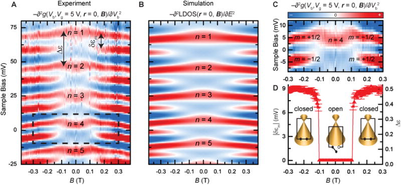
(A). Differential tunneling conductance map vs. magnetic field measured in the center of the graphene resonator for the n=1 to n=5 modes, indicated by the yellow dashed line in Fig. 2D. New resonances suddenly appear at a critical magnetic field of Bc ≈ ±0.11 T in between those present at B = 0 T. (B) Calculated local density of states (LDOS) of the graphene resonator states in a magnetic field to compare with experiment in (A) using a parabolic confining potential with κ = 10 eV/μm2 and Dirac point ED = 137 meV (Fig. 2D). (C) Magnified view of the n = 4 resonance from (A) showing the Berry-phase induced jumping of the m = ±1/2 modes with magnetic field: m = +1/2 only jumps at positive fields, and m = −1/2 only at negative fields. The 2D maps in A-C are shown in the 2nd derivative to remove the graphene dispersive background. (D) The difference in energy between the m = ±1/2 states, δεm, for the n = 4 resonance vs. magnetic field. The right axis is in units of the energy difference between the n=4 and n=3 resonances, Δε, at B = 0 T. The uncertainty reported represents one standard deviation and is determined by propagating the uncertainty resulting from a least square fit of Lorentzian functions used to determine the peak position of the resonator modes. The Dirac cones schematically illustrate the switching action: At low fields, the switch is open with zero Berry phase. When the critical field is reached, a π Berry phase is turned on closing the switch.
A simple understanding of the sudden jump in energy observed in the experiment (Fig. 3A) can be drawn from the Bohr-Sommerfeld quantization rule, which determines the energy levels En:
| (1) |
Here q and p are the canonical coordinates and momenta, respectively, ħ is Planck's constant divided by 2π, φB is the Berry phase accumulated in each orbital cycle, CR is a phase-space contour described below, and γ is a constant, the so-called Maslov index (5). The orbits are obtained from the semiclassical Hamiltonian H = En = υF|Π| + U(r), with U(r) the confining potential and Π = p – eA the kinetic momentum (e is the electron charge and A the vector potential). At zero magnetic field, states with opposite angular momenta ±m are degenerate, and their orbits are time-reversed images of one another (Fig. 1C, left). When a small magnetic field is turned on, the Lorentz force bends the paths of the +m and –m charge carriers in opposite directions, breaking the time-reversal symmetry and slightly lifting the orbital degeneracy. Crucially, at a critical magnetic field Bc, the orbit with angular momentum anti-parallel to the field is twisted by the Lorentz force into a qualitatively different “skipping” orbit (Fig. 1C, right). At this transition, the momentum-space trajectory, defined below, encloses the Dirac point, and φB discontinuously jumps from 0 to π; states with ±m, which are degenerate at B = 0, are abruptly pulled apart by half a period.
The intuitive picture described above can be made rigorous by using the Einstein-Brillouin-Keller (EBK) quantization (29, 30). Besides being more rigorous, EBK quantization facilitates visualization of the trajectory of Π along a semiclassical orbit, particularly because the orbits are quasiperiodic. In central force motion, the particle's orbit takes place in an annulus between the two classical turning points, and because the momentum in this annulus is two-valued, one can define a torus on which the momentum is uniquely determined [Section I of (27)]. The EBK quantization rules are formed by evaluating ∮ p · dq along the two topologically distinct loops on this torus, CR and Cθ (Fig. 1D). The EBK rule along Cθ gives the half-integer quantization of angular momentum; that along CR (Eq. 1) determines the energy levels for a given angular momentum. The Berry phase term in Eq. 1 is determined by the winding number of Π about the origin, evaluated on CR. Below Bc, the azimuthal component of Π has the same sign along CR (Fig. 1E, left): the corresponding II-space loop (Fig. 1B, blue curve) does not enclose the origin and the Berry phase is zero. Above Bc, however, II has a sign change along CR (Fig. 1E, right): the loop encircles the Dirac point and the Berry phase is π (Fig. 1B, red curve). Fig. 1B provides an intuitive visualization of the switching mechanism: the changing magnetic field shifts the Π-space contour, and at Bc it slips it over the Dirac cone apex, instantly changing the right side of Eq. 1 by π and shifting the energy levels accordingly [see Movie S1].
The semiclassical picture additionally allows us to estimate the strength of the critical field Bc necessary to switch the Berry phase (16). The value of Bc, which is sensitive to the confining potential profile, is obtained by finding the field strength B necessary to bend the electron orbit into a skipping orbit at the outer return point ro, thus resulting in zero azimuthal momentum: Πθ = mħ/ro − eBcro/2 = 0. For a parabolic potential U(r) =κr2, which accurately describes the low energy resonances (16), one obtains a simple expression:
| (2) |
where ε is the energy of the orbit. Using κ = 10 eV/μm2 obtained from a parabolic fitting of the potential profile (see Fig.2D) and ε = 65 meV (relative to the position of the Dirac point), which corresponds to the (m = 1/2, n = 1) state in Fig.3A, we find Bc = 0.1 T, in excellent agreement with the magnetic field values measured in the experiment.
A detailed comparison between experiment and theory can be made by solving the 2D Dirac Equation describing graphene electrons in the presence of a confining potential U(r) and a magnetic field B, [υF(σ · Π) + U(r)]Ψ(r) = εΨ(r) Following the semiclassical discussion above, we use a simple parabolic potential model U(r) = κr2, with κ = 10 eV/μm2 to fit the experimental data. The calculated local density of states (LDOS) at the center of the resonator [see Section I of (27) for details (27)] is in good agreement with the experiment (Figs. 3, A and B) and exhibits the half-period jumps between time-reversed states at similar magnetic field values.
Equation 2 also predicts a higher critical field for larger m states, as a larger Lorentz force is needed to induce skipping orbits. These larger angular momentum states have zero wavefunction weight at r = 0 (see Fig.2C), but can be probed at positions away from the center of the resonator (14, 15). Figure 4A shows the spectral conductance map measured at a position of 70 nm away from the center of the p-n junction resonator [see fig. S12 for additional measurements off center], and Fig. 4B shows the calculated LDOS at the same position. Much more complex spectral features are seen in comparison with the on-center measurement (Fig. 3A), which is sensitive only to the m = ±1/2 states. First, at B = 0, twice as many resonances are observed within the same energy range when compared to Fig. 3A. This confirms that additional m states are contributing to the STM maps. Second, both the theory and experimental maps exhibit a “stair case” pattern. Such an arrangement results from an overlap between the field-jumped m state and the next higher non-jumped m state, which are nearly degenerate in energy. For example, at positive fields, the field jumped m = 1/2 state overlaps in energy with the non-jumped m = 3/2 state, giving rise to a strong intensity at this energy. Figures 4, C and D illustrate this effect by showing separately the m= 1/2 and m = 3/2 contributions to the total density of states, respectively; Bc is indicated with a dashed line. In a similar fashion, this behavior continues for all adjacent m levels resulting in the series of staircase steps in the measured and calculated conductance maps in Fig. 4, A and B. Since the states jump by the half of the energy spacing, the staircase patterns can visually form upward and downward looking lines depending on subtle intensity variations at the transitions. For instance, while Fig. 4A shows mostly downward staircase patterns, other measurements (fig. S12) show both down and upward connections at the transitions; the parabolic potential model, Fig. 4B, shows an upward staircase. These behaviors depend on subtle effects, such as the potential shape in the off-center measurement, which are not relevant for our main discussion. More importantly, we plot, as a guide to the eye, Bc in Eq. 2 (dashed lines) for different values of m, showing excellent agreement with the semiclassical estimation above (note that upon summation in Fig. 4B, the positions of the steps, i.e. the white fringes, seem shifted to higher B values; this is expected and analogous to the peak shift observed when summing two Lorentzian functions). Overall, our one-parameter Dirac equation gives a very good description of the resonance dispersion, the critical field Bc, and its dependence on energy and momentum.
Fig. 4. Berry phase switching of higher angular momentum states.

(A) Differential tunneling conductance map vs. magnetic field measured 70 nm off-center of the graphene resonator. Kinks observed in the conductance correspond to the higher m modes which are seen to switch with higher critical magnetic fields. The staircase switching pattern results from m states that jump and overlap in energy the next higher non-switched m state, leading to an increased intensity at that energy (see text). Calculated LDOS vs magnetic field for a position 70 nm off center in a graphene circular resonator for (B) all m states, (C) m = +1/2, and (D) m = + 3/2 . The fan of dashed lines are calculations for the critical magnetic field using Eq. 2 with κ = 10 eV/μm2 and ED = 137 meV and m values as: (A),(B) m = ± to m = ±7/2, and single m values indicated on top of (C,D). The maps are shown in the 2n derivative (arbitrary values). See fig. S12 for additional off-center measurements.
Implications of these results include possible use in helicity-sensitive electro-optical measurements at THz frequencies with the ability to switch circular-polarized optical signals with small modulations of magnetic fields on the order of 10 mT (Section III.C of (27)). These applications, in conjunction with the fidelity of fabricating a variety of p-n junction and other electrostatic boundaries with impurity doping of boron nitride in graphene heterostructures, will expand the quantum tool box of graphene-based electron optics for future studies and applications.
Supplementary Material
Figure S1: Identifying the eigenstates of a graphene circular resonator. The differential conductance measurement of the circular graphene resonator from Fig. 2D. The solid black line shows a quadratic potential with κ= 10 eV/μm2 and a Dirac point of 137 mV, which is used as a confining potential in the simulations. (A) The solid color lines indicate the family of states with a strong maximum, and common n value and increasing m values, originating at m=1/2 at r=0. These maxima make arcs which follow the outline of the confining potential. (B) The dashed color lines indicate the family of states with common m values and increasing n starting at n=0 at the top of the map. (C) Superimposing the two sets of colored lines from (A) and (B) show that the maxima observed in the conductance map are observed at the intersection of the colored lines and enumerate the main maxima in the (n,m) eigenstates for the resonator.
Figure S2: Two-valued momentum field and toroidal cross-section. (A) Top view of a calculated closed orbit, the same as in Fig. 1C, left. The inward and outward momentum vectors are shown schematically as red and blue arrows respectively. (B) A calculated pr(r) curve, with inward and outward motions colored red and blue respectively. The curve was calculated using κ =10 eV/μm2, , and ε = 54 meV, corresponding to a radial action of ∮prdr = ħπ.
Figure S3: Graphene resonator modes made by probe field-effect tip gating. (A) Circular p-n junctions are created and probed simultaneously in the STM tunneling junction. The p-n junction ring is created by the electric field developed between the graphene sample bias Vb and the grounded probe tip, which can invert the background density profile determined by the device back gate potential Vg, for sufficiently high sample biases. Klein scattering at oblique angles to the p-n junction boundary gives rise to confined whispering gallery modes (WGM) illustrated in the graphene plane (13). (B) Schematic tunnel diagram showing that the WGM modes appear in this portion of the gate map due to a 2nd tunneling channel aligned with the graphene Fermi level. The WGM are emptied one by one as the sample bias is increased, due to field-effect gating of the graphene, and can be seen as one traces up vertically in the gate maps. (C)-(L) Spectral maps consisting of -d2g/dVb2 tunneling intensity as a function of back gate potential on the horizontal axis, Vg = −7 V to 5 V, and the sample potential on the vertical axis, Vb = 0.3 V to 0.8 V. Positive values are colored red, and negative blue. The first few WGM modes are seen as a collection of peaks (red) in the fans going from the lower left to upper right, and correspond to the WGM' modes in Ref. (13). The modes are seen to split into two peaks in various regions of the maps as a result of the Berry phase switch described in the main text. The green circles in (G) highlight the area where the splitting can be seen in the B = −0.5 T map, which is analyzed in detail in Fig. S4 and S5.
Figure S4: Berry phase switching of graphene resonator modes made by field-effect tip gating. Tunneling conductance gate maps at (A) B = 0 T and (B) B = 0.5 T illustrating the splitting of the graphene resonator states in weak magnetic fields. States corresponding to n = 0, 1, and 2 are seen to split in (B), as indicated by the red arrows, and analyzed further in Fig. S5. The maps are shown as −d2g/dVb2 to remove the dispersive graphene background. Positive values are colored red, and negative blue. The critical field for Berry phase splitting depends on the potential strength (Eq. (2) in the main text). Hence, splitting is only observed in regions of the map where the potential is of sufficient strength forming a boundary in the left portion of the map in (B).
Figure S5: Splitting of graphene resonator modes made by tip field-effect gating in weak magnetic fields. (A) Line profiles (dots) at Vb = 0.3 V showing the splitting of the n = 0 mode vs. magnetic field obtained from the spectral maps in Fig. S4. The split peaks correspond to the m= ±1/2 states. The solid lines are fits to Gaussian functions used to extract the peak positions of the split resonator modes. (B) The difference in peak positions between the m= ±1/2 states, as obtained from (A), for the n = 0 and n =1 modes normalized to the zero field mode spacing vs. magnetic field. The uncertainty reported represents one standard deviation and is determined by propagating the uncertainty resulting from a least square fit of Gaussian functions to determine the peak position of the resonator modes. A transition in the range of B ≈ ±0.2 T is observed, and the energy difference reach magnitudes of ≈ 1/2 of the zero field mode spacing, in agreement with the mode splitting observed in the fixed graphene resonators made by hBN impurity doping (Fig. 3D of the main text).
Figure S6: The induced potential profile in the traveling graphene resonator. (A) The induced potential (blue) is shown in the gate map range with the sample bias Vb, 0 V to 0.8 V, and back gate voltage Vg, −7 V to 5 V, to cover the range of the measurement in Fig. S4. Note that the p-n junctions are not defined until higher sample bias are reached when the blue curves cross the Fermi level shown by the orange lines. (B) The induced potential as a function of gate voltage at Vb=0.4 eV. The calculations use the parameters described in reference (13).
Figure S7: Variation of the p-n junction potential radius in the traveling graphene resonator. The quadratic potential parameter, κ, used to describe the confining potential is obtained from fitting the potential profiles as in Fig. S6 over the interval of ±50 nm, as a function of sample bias and back gate voltage. The parameter increases, which implies a smaller radius resonator, as the gate voltage and sample bias are increased.
Figure S8: Graphene device fabrication. Optical image of a single-layer graphene (SLG) flake (black outline) on hBN (red outline) before (A) and after (B) deposition of gold contacts required for electrical contact and STM navigation to the SLG sample region. The dashed lines outline the boundary of metallic contact to graphene. (C) Raman spectrum recorded on graphene/BN (black) and on bare BN (red). The sharpness and intensity of the 2D peak is indicative of high-quality SLG. (D) Composite image comprising an optical micrograph of the navigation pad superimposed with AFM scans of the finished device and the path of the STM tip traveling from the landing spot to the graphene sample.
Figure S9: Atomic-scale imaging of graphene and Moiré lattice determination. (A). Large-scale atomically-resolved STM topograph of the graphene/hBN device displaying exceptional flatness and cleanliness of the sample surface (Vb = 300 mV, I = 300 pA, Vg = 5 V). (B) Enlarged view of a region of (A) highlighting the graphene honeycomb lattice. (C) Fast Fourier transform (FFT) of the experimental topograph in (A) displaying the graphene atomic Bragg peaks (red circles) as well as a short-wavelength Moiré superlattice (green circles) which also surrounds each Bragg peak (dotted green hexagons). The length and orientation of the moiré superlattice corresponds to an angular misorientation of θ≈29° between the graphene and the underlying hBN layer. (D) FFT of a simulated STM topograph of graphene and hBN misoriented at θ=29.31° to compare with (C), which reproduces the primary features of the experimental topograph.
Figure S10: Creating fixed graphene quantum dots with charged impurity doping of hBN. (Top) Schematic of the graphene device and measurement setup. The device consists of graphene on a substrate consisting of hBN (blue)/SiO2 (light purple)/Si (dark purple). (Bottom) The creation of the quantum dot follows the method in Refs. (14, 28) and proceeds as follows: (i) Neutral impurities reside within the hBN. (ii) A positive backgate voltage, Vg = 30 V, is applied between silicon and graphene. This electric backgate field, Eg (red field lines), draws negative charge into graphene, producing n-doping. (iii) A voltage pulse of Vb = 5 V is applied between the STM tip and graphene for a time t = 60 s. The voltage pulse ionizes hBN impurities directly below the STM tip. The ionized impurities and released charge rearrange to create an opposite field, Ed (blue field lines), to screen the external gate field. (iv) When the external gate is removed (or lowered), the charged impurities remain and act as an embedded gate, locally p-doping the graphene.
Figure S11: Sharpness of the On/Off Critical Field Threshold. (A) Magnified view of the n = 4 resonance from Fig. 3A in the main text, showing the asymmetric splitting of the m = ±1/2 modes with magnetic field. Traces of -d2g/dVb2 at B= −0.06 T and B= −0.252 T, displaying a single peak, and a double peaked spectrum, respectively, are shown overlaid on the map (yellow lines). (B) A series of differential conductance spectra vs. sample bias for different magnetic fields covering the negative critical field transition shown by the oval in (A). At the critical field, Bc= −0.108 T, a second peak corresponding to the m= −1/2 resonance suddenly appears above the background signal, signifying the On/Off Berry phase switching transition is very sharp.
Figure S12: Off-center spectral maps. Differential conductance maps vs. magnetic field measured at distances of 40 nm to 90 nm from the center of the graphene resonator. States with higher m modes have more weight at positions farther away from the center of the p-n junction ring, where multiple transitions are observed with increasing magnetic field consistent with predictions from Eq. (2) in the main text. Each map consists of a series of 321 spectra plotted vertically as a function of magnetic field. The maps are shown in the 2nd derivative (arbitrary values). Positive values are colored red, and negative blue.
Movie S1: Evolution of graphene resonator orbits through the critical field. (Left). Calculated graphene electron orbits in a quadratic potential with angular momentum states m = −1/2 (blue) and m = +1/2 (red). The initial radial position (at the inner turning point) is chosen so that the radial action Jr = ∮ drpr(r) = h/2 for all frames, and the particle orbits for 1 ps. Parameters are υF = 106 m/s, κ = 10 eV/μm2 [see Section 1B]. (Right) Above, the kinematic momentum Π, as evaluated along Cr described in the main text, for the trajectories shown on the left. The momentum contours are plotted on the Dirac cone (brown) using the kinetic energy T(Π) = υF|π|. The Π-values plotted are the dynamically calculated radial and azimuthal momentum during the orbit. Below, a plot of Berry phase vs. magnetic field for the two orbits.
Acknowledgments
F.G., D.W., C.G., and Y. Z. acknowledges support under the Cooperative Research Agreement between the University of Maryland and the National Institute of Standards and Technology Center for Nanoscale Science and Technology, Grant No. 70NANB10H193, through the University of Maryland. J.W. acknowledges support from the Nation Research Council Fellowship. F. D. N. greatly appreciates support from the Swiss National Science Foundation under project number PZ00P2_167965. Y. Z. acknowledges support by the National Science Foundation of China under project number 11674150 and the National 1000 Young Talents Program. J.F.R.-N. acknowledges support from the NSF grant DMR-1507806. K.W. and T.T. acknowledge support from JSPS KAKENHI grant no. JP15K21722. L.S.L. acknowledges support by the Center for Integrated Quantum Materials (CIQM) under NSF award 1231319 and by the Center for Excitonics, an Energy Frontier Research Center funded by the U.S. Department of Energy, Office of Science, Basic Energy Sciences, under award no. DESC0001088. We thank Steve Blankenship and Alan Band for their contributions to this project, and we thank Michael Zwolak and Mark Stiles for valuable discussions.
Footnotes
References and Notes
- 1.Berry MV. Quantal Phase Factors Accompanying Adiabatic Changes. Proc R Soc Lond Math Phys Eng Sci. 1984;392:45–57. [Google Scholar]
- 2.Berry M. Anticipations of the Geometric Phase. Phys Today. 1990;43:34–40. doi: 10.1063/1.881219. [DOI] [Google Scholar]
- 3.Wilczek F, Shapere A. Advanced Series in Mathematical Physics. Vol. 5. WORLD SCIENTIFIC; 1989. Geometric Phases in Physics. http://www.worldscientific.com/worldscibooks/10.1142/0613. of. [Google Scholar]
- 4.Zwanziger JW, Koenig M, Pines A. Berry's Phase. Annu Rev Phys Chem. 1990;41:601–646. doi: 10.1146/annurev.pc.41.100190.003125. [DOI] [Google Scholar]
- 5.Xiao D, Chang MC, Niu Q. Berry phase effects on electronic properties. Rev Mod Phys. 2010;82:1959–2007. doi: 10.1103/RevModPhys.82.1959. [DOI] [Google Scholar]
- 6.Bitter T, Dubbers D. Manifestation of Berry's topological phase in neutron spin rotation. Phys Rev Lett. 1987;59:251–254. doi: 10.1103/PhysRevLett.59.251. [DOI] [PubMed] [Google Scholar]
- 7.Tycko R. Adiabatic Rotational Splittings and Berry's Phase in Nuclear Quadrupole Resonance. Phys Rev Lett. 1987;58:2281–2284. doi: 10.1103/PhysRevLett.58.2281. [DOI] [PubMed] [Google Scholar]
- 8.Chiao RY, Wu YS. Manifestations of Berry's Topological Phase for the Photon. Phys Rev Lett. 1986;57:933–936. doi: 10.1103/PhysRevLett.57.933. [DOI] [PubMed] [Google Scholar]
- 9.Tomita A, Chiao RY. Observation of Berry's Topological Phase by Use of an Optical Fiber. Phys Rev Lett. 1986;57:937–940. doi: 10.1103/PhysRevLett.57.937. [DOI] [PubMed] [Google Scholar]
- 10.Novoselov KS, et al. Two-dimensional gas of massless Dirac fermions in graphene. Nature. 2005;438:197–200. doi: 10.1038/nature04233. [DOI] [PubMed] [Google Scholar]
- 11.Zhang Y, Tan YW, Stormer HL, Kim P. Experimental observation of the quantum Hall effect and Berry's phase in graphene. Nature. 2005;438:201–204. doi: 10.1038/nature04235. [DOI] [PubMed] [Google Scholar]
- 12.Miller DL, et al. Observing the quantization of zero mass carriers in graphene. Science. 2009;324:924–927. doi: 10.1126/science.1171810. [DOI] [PubMed] [Google Scholar]
- 13.Zhao Y, et al. Creating and probing electron whispering-gallery modes in graphene. Science. 2015;348:672–675. doi: 10.1126/science.aaa7469. [DOI] [PubMed] [Google Scholar]
- 14.Lee J, et al. Imaging electrostatically confined Dirac fermions in graphene quantum dots. Nat Phys. 2016;12:1032–1036. doi: 10.1038/nphys3805. [DOI] [Google Scholar]
- 15.Gutiérrez C, Brown L, Kim CJ, Park J, Pasupathy AN. Klein tunnelling and electron trapping in nanometre-scale graphene quantum dots. Nat Phys. 2016;12:1069–1075. doi: 10.1038/nphys3806. [DOI] [Google Scholar]
- 16.Rodriguez-Nieva JF, Levitov LS. Berry phase jumps and giant nonreciprocity in Dirac quantum dots. Phys Rev B. 2016;94:235406. doi: 10.1103/PhysRevB.94.235406. [DOI] [Google Scholar]
- 17.Shytov AV, Rudner MS, Levitov LS. Klein Backscattering and Fabry-Pérot Interference in Graphene Heterojunctions. Phys Rev Lett. 2008;101:156804. doi: 10.1103/PhysRevLett.101.156804. [DOI] [PubMed] [Google Scholar]
- 18.Young AF, Kim P. Quantum interference and Klein tunnelling in graphene heterojunctions. Nat Phys. 2009;5:222–226. doi: 10.1038/nphys1198. [DOI] [Google Scholar]
- 19.Cheianov VV, Fal'ko V, Altshuler BL. The Focusing of Electron Flow and a Veselago Lens in Graphene p-n Junctions. Science. 2007;315:1252–1255. doi: 10.1126/science.1138020. [DOI] [PubMed] [Google Scholar]
- 20.De Martino A, Dell'Anna L, Egger R. Magnetic Confinement of Massless Dirac Fermions in Graphene. Phys Rev Lett. 2007;98:066802. doi: 10.1103/PhysRevLett.98.066802. [DOI] [PubMed] [Google Scholar]
- 21.Allain PE, Fuchs JN. Klein tunneling in graphene: optics with massless electrons. Eur Phys J B. 2011;83:301–317. doi: 10.1140/epjb/e2011-20351-3. [DOI] [Google Scholar]
- 22.Campos LC, et al. Quantum and classical confinement of resonant states in a trilayer graphene Fabry-Pérot interferometer. Nat Commun. 2012;3:1239. doi: 10.1038/ncomms2243. [DOI] [PubMed] [Google Scholar]
- 23.Varlet A, et al. Fabry-Pérot Interference in Gapped Bilayer Graphene with Broken Anti-Klein Tunneling. Phys Rev Lett. 2014;113:116601. doi: 10.1103/PhysRevLett.113.116601. [DOI] [PubMed] [Google Scholar]
- 24.Wu JS, Fogler MM. Scattering of two-dimensional massless Dirac electrons by a circular potential barrier. Phys Rev B. 2014;90:235402. doi: 10.1103/PhysRevB.90.235402. [DOI] [Google Scholar]
- 25.Garg NA, Ghosh S, Sharma M. Scattering of massless Dirac fermions in circular p-n junctions with and without magnetic field. J Phys Condens Matter. 2014;26:155301. doi: 10.1088/0953-8984/26/15/155301. [DOI] [PubMed] [Google Scholar]
- 26.Celotta RJ, et al. Invited Article: Autonomous assembly of atomically perfect nanostructures using a scanning tunneling microscope. Rev Sci Instrum. 2014;85:121301. doi: 10.1063/1.4902536. [DOI] [PubMed] [Google Scholar]
- 27.Additional supplementary text and data are available on Science Online
- 28.Velasco J, et al. Nanoscale Control of Rewriteable Doping Patterns in Pristine Graphene/Boron Nitride Heterostructures. Nano Lett. 2016;16:1620–1625. doi: 10.1021/acs.nanolett.5b04441. [DOI] [PubMed] [Google Scholar]
- 29.Einstein A. On the Quantum Theorem of Sommerfeld and Epstein. Deutshe Phys Ges. 1917;19:82–92. [Google Scholar]
- 30.Stone AD. Einstein's unknown insight and the problem of quantizing chaos. Phys Today. 2005;58:37–43. doi: 10.1063/1.2062917. [DOI] [Google Scholar]
- 31.Dean CR, et al. Boron nitride substrates for high-quality graphene electronics. Nat Nano. 2010;5:722–726. doi: 10.1038/nnano.2010.172. [DOI] [PubMed] [Google Scholar]
- 32.Ferrari AC. Raman spectrum of graphene and graphene layers. Phys Rev Lett. 2006;97:187401. doi: 10.1103/PhysRevLett.97.187401. [DOI] [PubMed] [Google Scholar]
Associated Data
This section collects any data citations, data availability statements, or supplementary materials included in this article.
Supplementary Materials
Figure S1: Identifying the eigenstates of a graphene circular resonator. The differential conductance measurement of the circular graphene resonator from Fig. 2D. The solid black line shows a quadratic potential with κ= 10 eV/μm2 and a Dirac point of 137 mV, which is used as a confining potential in the simulations. (A) The solid color lines indicate the family of states with a strong maximum, and common n value and increasing m values, originating at m=1/2 at r=0. These maxima make arcs which follow the outline of the confining potential. (B) The dashed color lines indicate the family of states with common m values and increasing n starting at n=0 at the top of the map. (C) Superimposing the two sets of colored lines from (A) and (B) show that the maxima observed in the conductance map are observed at the intersection of the colored lines and enumerate the main maxima in the (n,m) eigenstates for the resonator.
Figure S2: Two-valued momentum field and toroidal cross-section. (A) Top view of a calculated closed orbit, the same as in Fig. 1C, left. The inward and outward momentum vectors are shown schematically as red and blue arrows respectively. (B) A calculated pr(r) curve, with inward and outward motions colored red and blue respectively. The curve was calculated using κ =10 eV/μm2, , and ε = 54 meV, corresponding to a radial action of ∮prdr = ħπ.
Figure S3: Graphene resonator modes made by probe field-effect tip gating. (A) Circular p-n junctions are created and probed simultaneously in the STM tunneling junction. The p-n junction ring is created by the electric field developed between the graphene sample bias Vb and the grounded probe tip, which can invert the background density profile determined by the device back gate potential Vg, for sufficiently high sample biases. Klein scattering at oblique angles to the p-n junction boundary gives rise to confined whispering gallery modes (WGM) illustrated in the graphene plane (13). (B) Schematic tunnel diagram showing that the WGM modes appear in this portion of the gate map due to a 2nd tunneling channel aligned with the graphene Fermi level. The WGM are emptied one by one as the sample bias is increased, due to field-effect gating of the graphene, and can be seen as one traces up vertically in the gate maps. (C)-(L) Spectral maps consisting of -d2g/dVb2 tunneling intensity as a function of back gate potential on the horizontal axis, Vg = −7 V to 5 V, and the sample potential on the vertical axis, Vb = 0.3 V to 0.8 V. Positive values are colored red, and negative blue. The first few WGM modes are seen as a collection of peaks (red) in the fans going from the lower left to upper right, and correspond to the WGM' modes in Ref. (13). The modes are seen to split into two peaks in various regions of the maps as a result of the Berry phase switch described in the main text. The green circles in (G) highlight the area where the splitting can be seen in the B = −0.5 T map, which is analyzed in detail in Fig. S4 and S5.
Figure S4: Berry phase switching of graphene resonator modes made by field-effect tip gating. Tunneling conductance gate maps at (A) B = 0 T and (B) B = 0.5 T illustrating the splitting of the graphene resonator states in weak magnetic fields. States corresponding to n = 0, 1, and 2 are seen to split in (B), as indicated by the red arrows, and analyzed further in Fig. S5. The maps are shown as −d2g/dVb2 to remove the dispersive graphene background. Positive values are colored red, and negative blue. The critical field for Berry phase splitting depends on the potential strength (Eq. (2) in the main text). Hence, splitting is only observed in regions of the map where the potential is of sufficient strength forming a boundary in the left portion of the map in (B).
Figure S5: Splitting of graphene resonator modes made by tip field-effect gating in weak magnetic fields. (A) Line profiles (dots) at Vb = 0.3 V showing the splitting of the n = 0 mode vs. magnetic field obtained from the spectral maps in Fig. S4. The split peaks correspond to the m= ±1/2 states. The solid lines are fits to Gaussian functions used to extract the peak positions of the split resonator modes. (B) The difference in peak positions between the m= ±1/2 states, as obtained from (A), for the n = 0 and n =1 modes normalized to the zero field mode spacing vs. magnetic field. The uncertainty reported represents one standard deviation and is determined by propagating the uncertainty resulting from a least square fit of Gaussian functions to determine the peak position of the resonator modes. A transition in the range of B ≈ ±0.2 T is observed, and the energy difference reach magnitudes of ≈ 1/2 of the zero field mode spacing, in agreement with the mode splitting observed in the fixed graphene resonators made by hBN impurity doping (Fig. 3D of the main text).
Figure S6: The induced potential profile in the traveling graphene resonator. (A) The induced potential (blue) is shown in the gate map range with the sample bias Vb, 0 V to 0.8 V, and back gate voltage Vg, −7 V to 5 V, to cover the range of the measurement in Fig. S4. Note that the p-n junctions are not defined until higher sample bias are reached when the blue curves cross the Fermi level shown by the orange lines. (B) The induced potential as a function of gate voltage at Vb=0.4 eV. The calculations use the parameters described in reference (13).
Figure S7: Variation of the p-n junction potential radius in the traveling graphene resonator. The quadratic potential parameter, κ, used to describe the confining potential is obtained from fitting the potential profiles as in Fig. S6 over the interval of ±50 nm, as a function of sample bias and back gate voltage. The parameter increases, which implies a smaller radius resonator, as the gate voltage and sample bias are increased.
Figure S8: Graphene device fabrication. Optical image of a single-layer graphene (SLG) flake (black outline) on hBN (red outline) before (A) and after (B) deposition of gold contacts required for electrical contact and STM navigation to the SLG sample region. The dashed lines outline the boundary of metallic contact to graphene. (C) Raman spectrum recorded on graphene/BN (black) and on bare BN (red). The sharpness and intensity of the 2D peak is indicative of high-quality SLG. (D) Composite image comprising an optical micrograph of the navigation pad superimposed with AFM scans of the finished device and the path of the STM tip traveling from the landing spot to the graphene sample.
Figure S9: Atomic-scale imaging of graphene and Moiré lattice determination. (A). Large-scale atomically-resolved STM topograph of the graphene/hBN device displaying exceptional flatness and cleanliness of the sample surface (Vb = 300 mV, I = 300 pA, Vg = 5 V). (B) Enlarged view of a region of (A) highlighting the graphene honeycomb lattice. (C) Fast Fourier transform (FFT) of the experimental topograph in (A) displaying the graphene atomic Bragg peaks (red circles) as well as a short-wavelength Moiré superlattice (green circles) which also surrounds each Bragg peak (dotted green hexagons). The length and orientation of the moiré superlattice corresponds to an angular misorientation of θ≈29° between the graphene and the underlying hBN layer. (D) FFT of a simulated STM topograph of graphene and hBN misoriented at θ=29.31° to compare with (C), which reproduces the primary features of the experimental topograph.
Figure S10: Creating fixed graphene quantum dots with charged impurity doping of hBN. (Top) Schematic of the graphene device and measurement setup. The device consists of graphene on a substrate consisting of hBN (blue)/SiO2 (light purple)/Si (dark purple). (Bottom) The creation of the quantum dot follows the method in Refs. (14, 28) and proceeds as follows: (i) Neutral impurities reside within the hBN. (ii) A positive backgate voltage, Vg = 30 V, is applied between silicon and graphene. This electric backgate field, Eg (red field lines), draws negative charge into graphene, producing n-doping. (iii) A voltage pulse of Vb = 5 V is applied between the STM tip and graphene for a time t = 60 s. The voltage pulse ionizes hBN impurities directly below the STM tip. The ionized impurities and released charge rearrange to create an opposite field, Ed (blue field lines), to screen the external gate field. (iv) When the external gate is removed (or lowered), the charged impurities remain and act as an embedded gate, locally p-doping the graphene.
Figure S11: Sharpness of the On/Off Critical Field Threshold. (A) Magnified view of the n = 4 resonance from Fig. 3A in the main text, showing the asymmetric splitting of the m = ±1/2 modes with magnetic field. Traces of -d2g/dVb2 at B= −0.06 T and B= −0.252 T, displaying a single peak, and a double peaked spectrum, respectively, are shown overlaid on the map (yellow lines). (B) A series of differential conductance spectra vs. sample bias for different magnetic fields covering the negative critical field transition shown by the oval in (A). At the critical field, Bc= −0.108 T, a second peak corresponding to the m= −1/2 resonance suddenly appears above the background signal, signifying the On/Off Berry phase switching transition is very sharp.
Figure S12: Off-center spectral maps. Differential conductance maps vs. magnetic field measured at distances of 40 nm to 90 nm from the center of the graphene resonator. States with higher m modes have more weight at positions farther away from the center of the p-n junction ring, where multiple transitions are observed with increasing magnetic field consistent with predictions from Eq. (2) in the main text. Each map consists of a series of 321 spectra plotted vertically as a function of magnetic field. The maps are shown in the 2nd derivative (arbitrary values). Positive values are colored red, and negative blue.
Movie S1: Evolution of graphene resonator orbits through the critical field. (Left). Calculated graphene electron orbits in a quadratic potential with angular momentum states m = −1/2 (blue) and m = +1/2 (red). The initial radial position (at the inner turning point) is chosen so that the radial action Jr = ∮ drpr(r) = h/2 for all frames, and the particle orbits for 1 ps. Parameters are υF = 106 m/s, κ = 10 eV/μm2 [see Section 1B]. (Right) Above, the kinematic momentum Π, as evaluated along Cr described in the main text, for the trajectories shown on the left. The momentum contours are plotted on the Dirac cone (brown) using the kinetic energy T(Π) = υF|π|. The Π-values plotted are the dynamically calculated radial and azimuthal momentum during the orbit. Below, a plot of Berry phase vs. magnetic field for the two orbits.