Abstract
We investigated the influence of low-concentration indium (In) doping on the chemical and structural properties of solution-processed zinc oxide (ZnO) films and the electrical characteristics of bottom-gate/top-contact In-doped ZnO thin-film transistors (TFTs). The thermogravimetry and differential scanning calorimetry analysis results showed that thermal annealing at 400 °C for 40 min produces In-doped ZnO films. As the In content of ZnO films was increased from 1% to 9%, the metal-oxygen bonding increased from 5.56% to 71.33%, while the metal-hydroxyl bonding decreased from 72.03% to 9.63%. The X-ray diffraction peaks and field-emission scanning microscope images of the ZnO films with different In concentrations revealed a better crystalline quality and reduced grain size of the solution-processed ZnO thin films. The thickness of the In-doped ZnO films also increased when the In content was increased up to 5%; however, the thickness decreased on further increasing the In content. The field-effect mobility and on/off current ratio of In-doped ZnO TFTs were notably affected by any change in the In concentration. Considering the overall TFT performance, the optimal In doping concentration in the solution-processed ZnO semiconductor was determined to be 5% in this study. These results suggest that low-concentration In incorporation is crucial for modulating the morphological characteristics of solution-processed ZnO thin films and the TFT performance.
Keywords: oxide semiconductor, sol-gel precursor, solution process, doping, transistor
1. Introduction
Zinc oxide (ZnO) has been extensively studied over the past few decades because it has a large direct band gap energy (3.4 eV), a high exciton binding energy (60 meV), resource availability, and nontoxicity [1,2]. Since its band gap corresponds to UV light (with an approximate wavelength of 365 nm), ZnO is inherently transparent and has an optical transparency of over 85% in the visible light region. Thus, this material can be used in various electronic and optoelectronic devices. Further, ZnO is a well-known binary II–VI semiconductor compound and it is widely used in various ternary and quaternary oxide semiconductors such as zinc tin oxide, indium zinc oxide, and indium gallium zinc oxide. Research is being carried out to improve the electrical characteristics of thin-film transistors (TFTs) fabricated with these oxide semiconductors, and pioneering work has been reported on oxide TFT-driven organic light-emitting diode displays [3,4].
ZnO thin films are usually prepared by various deposition techniques such as atomic layer deposition, pulsed laser deposition, chemical vapor deposition, and sol-gel and sputtering methods [5,6,7,8,9]. Among these, the sol-gel technique has notable advantages over the others, as it offers process simplicity, low-cost manufacturing, and high throughput. This solution-based process is thus believed to be useful for large-area, low-cost manufacture of flexible electronics. However, the performance of solution-processed ZnO TFTs is generally inferior to that of vacuum-processed devices. For example, Brox-Nilsen et al. reported saturation mobility values of over 50 cm2/Vs in the ZnO TFTs fabricated by radio-frequency magnetron sputtering at room temperature [10]. Lin et al. reported a saturation mobility of 2–4 cm2/Vs in ZnO TFTs processed via spin coating [11]. The most common mobility of solution-processed ZnO TFTs is in the range of 0.1 cm2/Vs to several cm2/Vs; as a result, low-level integrated circuits of solution-processed TFTs seem adequate for low-end sensors and disposable chips. Such low mobilities of these transistors are intimately associated with the morphological and structural characteristics of solution-processed semiconductor films. Here, the solidification phenomenon in solution-deposited films should be distinguished from the morphological growth in vacuum-deposited films [12]. In vacuum deposition processes, nucleation occurs from the nuclei on the surface of the substrate, allowing sequential bottom-up growth of the film. In contrast, solutes can be accommodated near the bulk and surface of the solution-deposited film while substrate heating causes the solidification to proceed at the bottom. This complexity ultimately leads to the formation of grain boundaries in polycrystalline ZnO thin films deposited through solution processes. Note that grain boundaries in solution-processed ZnO semiconductor films can be a major constraint factor for the TFT performance because they act as trapping centers for mobile charge carriers. Therefore, analyses of the morphological and structural characteristics of solution-processed ZnO films are very important to understand the charge transport behavior of these films and the TFT performance.
The extrinsic doping of ZnO was first investigated in the 1950s [13]. Recent years have seen increased interest in the extrinsic doping phenomenon because high free carrier concentrations and low electrical resistivities can be achieved by the extrinsic doping of ZnO. This is possible because the free carrier concentration and electrical resistivity of ZnO can be controllably engineered by extrinsic doping, which is a prerequisite for its use in electronic devices. Recent studies demonstrated that group IIIB elements such as boron, aluminum (Al), gallium, and indium act as shallow donors in ZnO when they are incorporated on Zn cation sites; the outer p electron of these group IIIB elements is weakly bound in the ZnO lattice, allowing it to be thermally ionized into the conduction band of ZnO [14]. Among these dopants, In-doped ZnO thin films have attracted more focus owing to their superior properties in terms of electrical conductivity, optical transparency, and chemical stability compared to those of undoped ZnO thin films [15,16]. In addition, taking into account the ionic radii, it is clear that In (the ionic radius of In3+ is ~80 pm) is best suited to substitute Zn (ionic radius of Zn2+ ~ 74 pm) in the ZnO lattice [17,18]. Rokn-Abadi et al. reported better optical and electrical properties of the solution-processed ZnO film by doping it with 2%, 4%, 8% and 16% In concentrations [19]. Singh et al. reported that the minimum electrical resistivity values of the order of 0.045 Ωm could be obtained for solution-processed ZnO films with a 5% In dopant concentration [20]. Biswal et al. reported a reduction in the electrical resistivity of In-doped ZnO films deposited by the ultrasonic chemical spray method, with [In]/[In + Zn] atomic percent ratios of 1.5, 3.0, and 4.0 at. % [7]. These previous studies on In doping in solution-processed ZnO films focused mostly on the electrical, optical, and structural characteristics of the films. Nevertheless, there is still a lack of understanding on the effects of low-concentration In doping on the performance of solution-processed ZnO TFTs. Noteworthy is the significant effect of In doping in ZnO films on the performance of TFTs fabricated using a sputtering system; Cheremisin et al. demonstrated that the low-level In doping of ZnO films is effective to modify the film morphology, thereby contributing to increasing the field-effect mobility and decreasing the threshold voltage of vacuum-processed TFTs [21]. Accordingly, a comprehensive study on the morphological and structural characteristics of In-doped ZnO films deposited by a solution process together with the electrical characteristics of solution-processed In-doped ZnO TFTs is essential for further advancement of this technology.
In this study, we investigated the effects of low-concentration In doping on the chemical and structural characteristics of solution-processed ZnO films. The doping concentration of In in ZnO films was varied from 1–9%. The In-doped ZnO sols and films were analyzed by thermogravimetry coupled with differential scanning calorimetry, X-ray photoemission spectroscopy, X-ray diffraction, and scanning electron microscopy. Bottom-gate/top-contact In-doped ZnO TFTs were fabricated by spin coating, and the electrical characteristics of these TFTs were investigated by analyzing the on/off current ratio and the field-effect mobility. The experimental results demonstrate the significant impact of low-concentration In doping of solution-processed ZnO semiconductor films on the TFT performance.
2. Experimental
The In-doped ZnO thin films were prepared by a sol-gel spin coating method. Zinc nitrate hydrate (Zn(NO3)2·xH2O) (Sigma-Aldrich, Yongin, Korea) and indium nitrate hydrate (In(NO3)3·xH2O) (Sigma-Aldrich) were used as precursors. The atomic percentage of In to Zn was varied from 1% to 9% by varying the stoichiometric quantity of In(NO3)3·xH2O with respect to Zn(NO3)2·xH2O. The precursor sols were prepared by dissolving the nitrate salts in 2-methoxyethanol (Sigma-Aldrich) at 75 °C for 4 h and filtered through a 0.2 μm polytetrafluorethylene syringe filter.
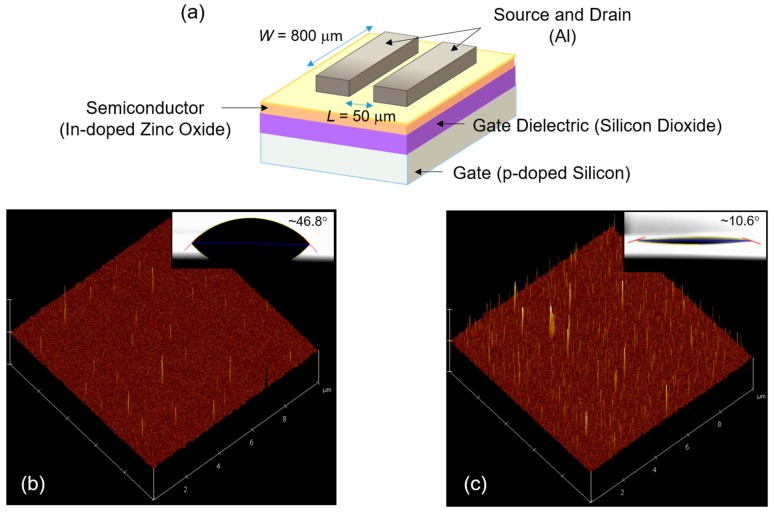
Figure 1a shows the schematic representation of the fabricated In-doped ZnO TFTs. A heavily boron (p+)-doped silicon substrate with a 100-nm-thick silicon dioxide (SiO2) dielectric layer (LG Siltron, Seoul, Korea) was used for the fabrication of bottom-gate and top-contact In-doped ZnO TFTs. In order to improve the chemical compatibility of the interface between the dielectric and semiconductor layers we hydrophilized the surface of the SiO2 gate dielectric by O2 plasma (40 W, 9 SCCM) for 10 s. Figure 1b,c show the surface properties of pristine and O2 plasma-treated SiO2 dielectric layers, respectively. It is observed that the surface of the SiO2 dielectric layer became rougher and more wettable owing to the O2 plasma treatment.
Figure 1.
(a) Schematic representation of the fabricated In-doped ZnO TFT having the channel length (L) and width (W) of 50 μm and 800 μm, respectively. Atomic force microscope images (10 × 10 μm) of the (b) pristine and (c) O2 plasma-treated SiO2 dielectric layers. The insets show the contact angles of both layers.
The root-mean-square surface roughness values were approximately 10.1 nm for the pristine SiO2 layer and approximately 17.7 nm for the O2 plasma-treated SiO2 layer. From the measured contact angles of the distilled-water drops, the surface energies were calculated to be approximately 51.8 mJ/m2 for the pristine SiO2 layer and approximately 71.8 mJ/m2 for the O2 plasma-treated SiO2 layer; the surface free energy of distilled water was assumed to be 73.0 mJ/m2 [22]. Subsequently, the In-doped ZnO precursor sols were spin-coated on the SiO2/Si substrates at a speed of 4000 rpm for 35 s. The coated films were pre-heated on a hot-plate at 120 °C for 5 min and then annealed in a furnace at 400 °C for 40 min. Finally, source and drain electrodes (Al) were thermally deposited on the semiconductor layer through a shadow mask with a channel length (L) and width (W) of 50 μm and 800 μm, respectively.
Thermogravimetric analysis (TGA) (N-1000, Sinco, Seoul, Korea) and differential scanning calorimetry (DSC) (Setaram, DSC 131 Evo, Caluire, France) were performed under a nitrogen atmosphere at a heating rate of 10 °C/min. The chemical characteristics of the In-doped ZnO films were investigated by X-ray photoelectron spectroscopy (XPS) (K-Alpha, Thermo Scientific, Waltham, MA, USA), and the crystallographic properties were characterized by X-ray diffraction (XRD) (DMAX-2500, Rigaku, Tokyo, Japan). The surface morphologies of the films were examined by atomic force microscope (AFM) (XE150, PSIA, Santa Clara, CA, USA) and field-emission scanning electron microscopy (FESEM) (S-4300, Hitachi, Ibaraki, Japan). The electrical characteristics of the TFTs were evaluated using a semiconductor analyzer (4200-SCS, Keithley, Seoul, Korea).
3. Results and Discussion
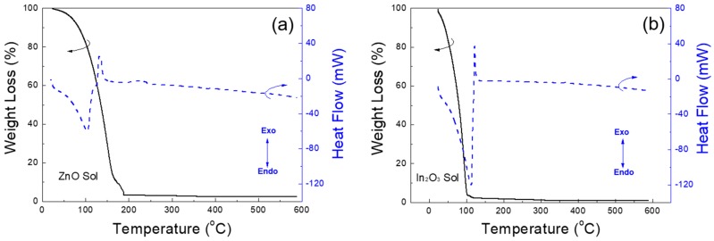
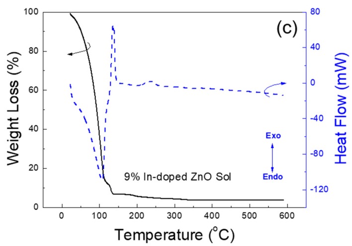
Simultaneous thermal analyses (TGA-DSC) were performed at a scanning rate of 10 °C/min from room temperature to 590 °C under nitrogen, to compare the thermal decomposition of ZnO, indium oxide (In2O3) and 9% In-doped ZnO sols. Figure 2 shows the TGA-DSC curves of these specimens. From Figure 2, the first endothermic reactions were observed with large weight losses in the range of 25–200 °C. These weight losses are attributed primarily to the low temperature solvent evaporation and precursor decomposition. In these sols, In(NO3)3·xH2O and Zn(NO3)2·xH2O had decomposed and hydrolyzed to In(OH)3 and Zn(OH)2, respectively. Because In3+ has a larger orbital radius and lower binding energy than Zn2+, the temperatures of the first weight loss would decrease with increased indium content [23]. In our results, as shown in Figure 2a–c, the abrupt weight loss continued to the temperatures of approximately 190, 120 and 132 °C for the ZnO, In2O3, and 9% In-doped ZnO sols, respectively. In the meantime, large exothermic peaks were observed at approximately 150 °C and then the weight loss became gradual. This can be rationalized by the alloying and dehydration of the metal hydroxides to the multi-component oxides [24]. It is well known that the exothermic peaks in the DSC curves with small weight losses correspond to the crystallization of each specimen and the decomposition of the residual organic materials [1]. On the other hand, no meaningful weight losses were detected beyond 400 °C for all the sols. Therefore, we could confirm that an annealing temperature of 400 °C is sufficient to convert the precursors into semiconducting films.
Figure 2.
TGA-DSC curves of the (a) ZnO; (b) In2O3 and (c) 9% In-doped ZnO sols, respectively.
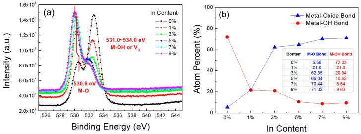
X-ray photoelectron spectral analysis was performed to examine the effect of In doping on the chemical-bonding states of the ZnO films. Figure 3a shows the O 1s peaks of ZnO and In-doped ZnO thin films. The O 1s peaks of the In-doped ZnO films shifted slightly toward a lower binding energy, as the In content increased. These peak shifts are attributed to the difference in the bond lengths of In-O (0.210 nm) and Zn-O (0.197 nm), which resulted in the decreases in the binding energy of the O 1s peaks. These peak shifts are consistent with those reported by Martha et al. [25]. The asymmetric peaks observed in the O 1s spectra could be deconvoluted into two peaks. The lower binding energy peaks near 530.6 eV are attributed to the lattice oxygen atoms of the In-O and Zn-O chemical bonds. However, the shoulders in the spectral region between 531.0 and 534.0 eV are attributed to oxygen deficiency and the hydroxide group, which originate from the oxygen vacancy (VO) and the surface-adsorbed hydroxyl oxygen atoms (M-OH) [26]. Figure 3b shows the results from the deconvoluted XPS spectra of O 1s for the ZnO and In-doped ZnO thin films. Notably, as the In content increased, the quantity of the oxide (M-O) bonds increased from 5.56% to 71.33% and that of the hydroxyl (M-OH) ones decreased from 72.03% to 9.63%, indicating a increase in the fully coordinated metal sites and a decrease in the hydroxyl groups. This is probably due to the additional supply of oxygen atoms from In2O3, and the difference in the crystallization temperatures of ZnO and In2O3 thin films, as shown in Figure 2, resulting in the formation of In-doped ZnO thin films under the same annealing temperature.
Figure 3.
(a) O 1s XPS spectra of the In-doped ZnO films with different In concentrations; (b) Atom percent of metal-oxide bonds and metal-OH bonds in In-doped ZnO thin films.
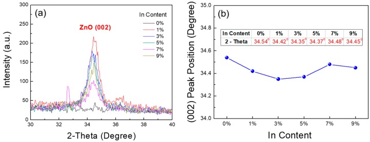
In order to investigate the crystallinity of the In-doped ZnO thin films, the precursor sols with different In contents were spin-coated on SiO2/Si substrates and annealed at 400 °C. The XRD in a 2θ-scan mode was used to understand the crystalline structure of the fabricated films. As shown in Figure 4a, the (002) diffraction peaks of the ZnO thin films were found with the doping of In, which indicates that In doping improves the crystalline quality of the ZnO thin films. The peaks became broad and the intensity of the (002) diffraction peaks gradually decreased as the In concentration was increased further, which indicates that the crystallinity of the In-doped ZnO films also depends on the elemental content and/or composition of the films. Similar results have been reported by other researchers [25,27]. In Figure 4b, it is observed that all the ZnO (002) diffraction peaks have shifted to smaller angles. This implies that the replacement of Zn2+ ions with In3+ ions is accompanied by lattice expansion, because the ionic radius of In3+ (80 pm) is larger than that of Zn2+ (74 pm) [17,18].
Figure 4.
(a) XRD patterns and (b) the (002) peak positions of the fabricated films with different In contents.
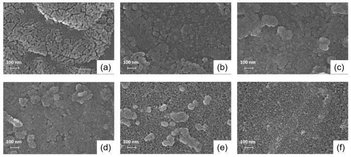
Figure 5 shows the top-view FESEM images of the In-doped ZnO thin films with different In contents. As shown in the micrograph (Figure 5a), the surface of the undoped ZnO film shows many cracks. The number of cracks and the roughness of the ZnO films decreased with the increase in the In content. This suggests that In doping has a significant influence on the surface morphology of the solution-processed ZnO film. As the In content increased from 0% to 9%, the grain size of the films decreased obviously. This phenomenon can be attributed to the different ionic radii of the In3+ and Zn2+ ions. Noteworthy is that the thickness of the In-doped ZnO films increased with the increasing In content up to 5%, and then decreased upon a further increase in the In content. In our results, the thicknesses of the fabricated films were 13.5, 42, 56, 64, 29.7, and 31.1 nm for undoped and 1%, 3%, 5%, 7% and 9% In-doped ZnO thin films, respectively. Likewise, it has also been reported in the literature that the morphology and the crystallinity of the In-doped ZnO films can be changed by the In content. Kim et al. reported that the crystal quality of In-doped ZnO films is enhanced by the incorporation of adequate amounts of In, which is explained by the migration velocity of In being faster than that of Zn and O atoms in the ZnO film due to the In-O bond being weaker than the Zn-O bond [28]. Here, we assume that In3+ ions act as Frenkel defects when their content is less than 5% in the primary ZnO structure, indicating that In3+ ions place in interstitial sites in the ZnO film. On the other hand, In3+ ions prefer to substitute the host Zn atoms and thus act as substitutional impurities when their content exceeds 7%. It is thought that more defect creation energy is required with increasing the In content in the primary ZnO structure, thereby limiting the formation of Frenkel defects in the film. Considering that the ZnO crystal region around an In impurity can be distorted, the lattice possibly becomes more strained around interstitial In3+ ions compared to the substitutional In3+ ion case; neighboring host atoms will be pushed away if an impurity atom is larger than the host atom [29]. This might cause the increase in the thickness of the In-doped ZnO films with increasing the In content up to 5%. However, the threshold defect creation energy could not be deduced in this study. We expect that further studies using inelastic laser spectroscopy, such as Raman and Brillouin, will be useful to clarify the influence of In content on the energetic state and the distribution of In3+ ions in the In-doped ZnO films.
Figure 5.
FESEM images of the (a) undoped; (b) 1%; (c) 3%; (d) 5%; (e) 7% and (f) 9% In-doped ZnO films.
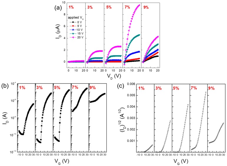
To examine the electrical characteristics of the In-doped ZnO thin films, bottom-gate/top-contact ZnO TFTs with SiO2/Si substrates were fabricated. In this study, the ZnO TFT did not function as TFTs, even after annealing at 600 °C, due to the very thin nature (approximately 13.5 nm) of the solution-processed ZnO semiconductor film. Note that the electrical resistance of the ZnO semiconductor increased with the decreasing film thickness, and a rather thicker ZnO film is required for TFT operation [30,31]. To emphasize the effect of film thickness on the TFT performance, it will be useful to vary the thickness of solution-processed oxide semiconductor films without altering their chemical and morphological properties. Figure 6a shows the output characteristics of In-doped ZnO TFTs with different In contents. These output characteristics were measured by changing the drain voltage (VD) from 0 to 20 V in increments of 1 V at different gate voltages (VG). The drain current (ID) increased when the In content was increased up to 7% and then decreased when the In content was further increased. Considering the variation in the film thickness according to the In content, the observed change in ID of In-doped ZnO TFTs is believed to be influenced by the electrical properties of the In-doped ZnO semiconductor films, rather than the effect of the film thickness. Herein, the enhanced conductivities of the In-doped ZnO TFTs could be explained by the larger s orbital of In3+, which renders the In-doped ZnO films more conductive, and the increased carrier concentration caused by the addition of the n-type dopant, In. Figure 6b,c show the transfer characteristics of In-doped ZnO TFTs with different In contents. These characteristics were measured at a fixed VD of 15 V, while VG was swept from –10 to 30 V in increments of 1 V. The electrical properties of the In-doped ZnO TFTs are summarized in Table 1. The on/off current ratio (Ion/Ioff) was estimated from ID vs. VG plots, as shown in Figure 6b. In our work, the 7% and 9% In-doped ZnO TFTs exhibited remarkably higher off-state currents (exceeding approximately 10−7 A) than those (approximately 10−11 A) of 3% and 5% In-doped ZnO TFTs. An enhancement in the electrical conductivity, i.e., a reduction in the resistivity, of the 7% and 9% In-doped ZnO semiconductors is the most likely explanation for these higher off-state currents. Note that a back-channel current conduction between source and drain electrodes in bottom-gate/top-contact structured TFTs, which is not controlled by VG, will dominate the off-state current when the resistivity of the channel layer is too low [32,33]. Previous studies have reported that the ideal resistivity of ZnO films for application in TFTs is about 105–106 Ωcm [34,35]. However, the difference in the on-state currents of these four TFTs seems less significant. As a result, the 5% In-doped ZnO TFT exhibited the highest Ion/Ioff value of 9.5 × 10⁵ in this study. For the 1% In-doped ZnO TFT case, it is reasonable to ascribe the lower on-state current to the higher resistance of the 1% In-doped ZnO semiconductor. We consider that a rather high off-state current (approximately 10−10 A) of this device is presumably due to deep donor-like states and their energetic distributions in the 1% In-doped ZnO semiconductor [36].
Figure 6.
(a) ID vs. VD; (b) ID vs. VG and (c) (ID)1/2 vs. VG plots of In-doped ZnO TFTs with different In contents.
Table 1.
Electrical characteristics of the In-doped ZnO TFTs with different In contents.
| In Concentration (%) | Thickness (nm) | μ (cm2/Vs) | VTh (V) | Ion/Ioff |
|---|---|---|---|---|
| 0 | 13.5 | - | - | - |
| 1 | 42 | 0.004 | 11.2 | 3.5 × 10³ |
| 3 | 56 | 0.07 | 9.9 | 5.4 × 10⁵ |
| 5 | 64 | 0.14 | 8.4 | 9.5 × 10⁵ |
| 7 | 29.7 | 0.16 | 4.9 | 5 × 10² |
| 9 | 31.1 | - | - | 10 |
Important TFT parameters such as the threshold voltage (VTh) and the field-effect mobility (μ) were further obtained from the (ID)1/2 vs. VG plots shown in Figure 6c. Based on the obtained transfer characteristics, μ in the saturation region was calculated using the following equation:
| (1) |
where Ci is the capacitance per unit area of the gate dielectric layer (34.52 nF/cm2). As the In content increased from 1% to 7%, it was clearly observed that VTh decreased from 11.2 to 4.9 V and μ increased from 0.004 to 0.16 cm2/Vs. Since the thickness of the 7% In-doped ZnO film is much smaller than those of 1%, 3% and 5% In-doped ZnO films, the enhanced TFT performance should also be interpreted in terms of the increased electron concentration and the enhanced conductivity owing to In doping in a ZnO semiconductor, as exemplified by other groups [23,37]. However, it was meaningless to evaluate the electrical properties of the 9% In-doped ZnO TFT because of the nonsaturating drain current and the floating off-state current, as shown in Figure 6a,b, respectively. The electrical conductivity of the 9% In-doped ZnO film is likely to be detrimental for the gate-field–induced current modulation at the semiconductor/dielectric interface. In this study, the optimal doping level of In in the solution-processed ZnO semiconductor is suggested to be 5% by taking into account the switching and amplification functions of TFTs. Nonetheless, the overall performance of the present 5% In-doped ZnO TFT fabricated by the solution process is still inferior to that of the TFTs in which the In-doped ZnO channel layer was deposited by a vacuum sputtering system [21]. This is possibly due to the rough surface of the O2 plasma-treated SiO2 dielectric layer and electron trapping at grain boundaries in the solution-processed In-doped ZnO semiconductor films. A nondestructive surface modification, such as the one obtained by the UV/ozone treatment, is expected to afford dielectric layers with a smooth surface [38]. Also, a high-pressure annealing will reduce the generation of defect states in solution-processed oxide semiconductors [39]. Further studies should focus on analyzing the charge transport behaviors in solution-processed oxide TFTs by using different physical models [40,41]. They may help in further enhancing the performance of solution-processed oxide TFTs, as well as in optimizing the material composition.
4. Conclusions
We fabricated solution-processed In-doped ZnO films with different concentrations (0%, 1%, 3%, 5%, 7%, and 9%) of the n-type dopant, In, using nitrate-based precursors. The XPS analyses of ZnO and In-doped ZnO films showed a shift in the O 1s peak toward a lower binding energy owing to the difference in the bond lengths of In-O and ZnO and an increase in the fully coordinated metal sites and a decrease in the hydroxyl groups. The (002) diffraction peak in the In-doped ZnO films implied an improved crystalline quality of the ZnO film, and its shift toward a lower angle with increasing In content indicated lattice expansion caused by replacing Zn2+ ions with In3+ ions. These results demonstrate the successful fabrication of In-doped ZnO films with different In concentrations. In addition, the surface morphology and thickness of In-doped ZnO films were significantly affected by the In concentration. A reduction in the cracks and a decrease in the grain size were observed as the In content was increased. An important observation was that the change in the film thickness was not proportional to the In concentration; the thicknesses of the fabricated films were 13.5, 42, 56, 64, 29.7, and 31.1 nm for undoped, 1%, 3%, 5%, 7%, and 9% In-doped ZnO thin films, respectively. Herein, it is assumed that In3+ ions act as Frenkel defects when their content is less than 5% in the primary ZnO structure, indicating that In3+ ions occupy the interstitial sites in the ZnO film. However, we consider that In3+ ions prefer to replace the host Zn atoms and thus act as substitutional impurities when their content exceeds 7%. For the In-doped ZnO TFTs, both the drain current and the field-effect mobility increased, while the threshold voltage decreased as the In content was increased up to 7%. However, the off-state currents of the 7% and 9% In-doped ZnO TFTs showed a large increase of beyond 10−7A, causing a significant reduction in the on/off current ratio to below 103. Consequently, the TFT performance can be interpreted in terms of the increased electron concentration and enhanced conductivity owing to In doping in a ZnO semiconductor, rather than the variation in the film thickness. We believe that these results can be useful in analyzing the effect of doping on the structural and electrical properties of solution-processed oxide semiconductors for application in TFTs.
Acknowledgments
This research was supported by the Hallym University Research Fund, 2017 (HRF-201701-014), the Leading Human Resource Training Program of Regional Neo Industry through the National Research Foundation of Korea (NRF) funded by the Ministry of Science, ICT and Future Planning (2016H1D5A1910427), and the Basic Science Research Programs through NRF funded by the Ministry of Education (2017R1D1A1B03034788).
Author Contributions
X.Z. and H.L. contributed equally to the fabrication of TFTs, the experimental measurements (TGA/DSC characteristics, crystalline and morphological characteristics, and electrical characteristics) and the writing of the manuscript. J.-H.K. and E.-J.K. contributed to the analysis of the XPS results of the fabricated films. J.P. supervised the whole procedure and also contributed to the analysis of the experimental results and the writing of the manuscript. All authors participated in the discussion and commented on the paper.
Conflicts of Interest
The authors declare no conflict of interest.
References
- 1.Choi C.G., Seo S.-J., Bae B.-S. Solution-processed indium-zinc oxide transparent thin-film transistors. Electrochem. Solid-State Lett. 2008;11:H7–H9. doi: 10.1149/1.2800562. [DOI] [Google Scholar]
- 2.Oh B.-Y., Kim Y.-H., Lee H.-J., Kim B.-Y., Park H.-G., Han J.-W., Heo G.-S., Kim T.-W., Kim K.-Y., Seo D.-S. High performance ZnO thin-film transistor fabricated by atomic layer deposition. Semicond. Sci. Technol. 2011;26:085007. doi: 10.1088/0268-1242/26/8/085007. [DOI] [Google Scholar]
- 3.Hsieh H.-H., Lu H.-H., Ting H.-C., Chuang C.-S., Chen C.-Y., Lin Y. Development of IGZO TFTs and their applications to next generation flat-panel displays. J. Inf. Disp. 2010;11:160–164. doi: 10.1080/15980316.2010.9665845. [DOI] [Google Scholar]
- 4.Nag M., Obata K., Fukui Y., Myny K., Schols S., Vicca P., Ke T.H., Smout S., Willegems M., Ameys M., et al. Flexible AMOLED display and gate-driver with self-aligned IGZO TFT on plastic foil. SID Symp. Dig. Tech. Pap. 2014;45:248–251. doi: 10.1002/j.2168-0159.2014.tb00068.x. [DOI] [Google Scholar]
- 5.Hausmann D.M., Kim E., Becker J., Gordon R.G. Atomic layer deposition of hafnium and zirconium oxides using metal amide precursors. Chem. Mater. 2002;14:4350–4358. doi: 10.1021/cm020357x. [DOI] [Google Scholar]
- 6.Taabouche A., Bouabellou A., Kermiche F., Hanini F., Menakh S., Bouachiba Y., Kerdja T., Benazzouz C., Bouafia M., Amara S. Effect of substrates on the properties of ZnO thin films growth by pulsed laser deposition. Adv. Mater. Phys. Chem. 2013;3:209–213. doi: 10.4236/ampc.2013.34031. [DOI] [Google Scholar]
- 7.Biswal R., Maldonado A., Vega-Perez J., Acosta D.R., De La M., Olvera L. Indium doped zinc oxide thin films deposited by ultrasonic chemical spray technique, starting from zinc acetylacetonate and indium chloride. Materials. 2014;7:5038–5046. doi: 10.3390/ma7075038. [DOI] [PMC free article] [PubMed] [Google Scholar]
- 8.Koo C.Y., Song K., Jun T., Kim D., Jeong Y., Kim S.-H., Ha J., Moon J. Low temperature solution-processed InZnO thin-film transistors. J. Electrochem. Soc. 2010;157:J111–J115. doi: 10.1149/1.3298886. [DOI] [Google Scholar]
- 9.Chang P.-C., Fan Z., Wang D., Tseng W.-Y., Chiou W.-A., Hong J., Lu J.G. ZnO nanowires synthesized by vapor trapping CVD method. Chem. Mater. 2004;16:5133–5137. doi: 10.1021/cm049182c. [DOI] [Google Scholar]
- 10.Brox-Nilsen C., Jin J., Luo Y., Bao P., Song A.M. Sputtered ZnO thin-film transistors with carrier mobility over 50 cm2/Vs. IEEE Trans. Electron Devices. 2013;60:3424–3429. doi: 10.1109/TED.2013.2279401. [DOI] [Google Scholar]
- 11.Lin Y.-H., Faber H., Labram J.G., Stratakis E., Sygellou L., Kymakis E., Hastas N.A., Li R., Zhao K., Amassian A., et al. High electron mobility thin-film transistors based on solution-processed semiconducting metal oxide heterojunctions and quasi-supperlattices. Adv. Sci. 2015;2:1500058. doi: 10.1002/advs.201500058. [DOI] [PMC free article] [PubMed] [Google Scholar]
- 12.Lee H., Zhang X., Hwang J., Park J. Morphological influence of solution-processed zinc oxide films on electrical characteristics of thin-film transistors. Materials. 2016;9:851. doi: 10.3390/ma9100851. [DOI] [PMC free article] [PubMed] [Google Scholar]
- 13.Hauffe K., Vierk A.L. Über die elektrische Leitfähigkeit von Zinkoxyd mit Fremdoxydzusätzen. Z. Phys. Chem. 1950;196:160–180. [Google Scholar]
- 14.Ellmer K., Bikowski A. Intrinsic and extrinsic doping of ZnO and ZnO alloys. J. Phys. D Appl. Phys. 2016;49:413002. doi: 10.1088/0022-3727/49/41/413002. [DOI] [Google Scholar]
- 15.Bel-Hadj-Tahar R., Mohamed A.B. Sol-Gel Processed Indium-Doped Zinc Oxide Thin Films and Their Electrical and Optical Properties. New J. Glass Ceram. 2014;4:55–65. doi: 10.4236/njgc.2014.44008. [DOI] [Google Scholar]
- 16.Lo C.Y., Hsu C.-L., Yu Q.-X., Lee H.-Y., Lee C.-T. Investigation of transparent and conductive undoped Zn2In2O5-x films deposited on n-type GaN layers. J. Appl. Phys. 2002;92:274. doi: 10.1063/1.1481207. [DOI] [Google Scholar]
- 17.Yu Y., Wang J., Li W., Zheng W., Cao Y. Doping mechanism of Zn2+ ions in Zn-doped TiO2 prepared by a sol-gel method. CrystEngComm. 2015;17:5074–5080. doi: 10.1039/C5CE00933B. [DOI] [Google Scholar]
- 18.Han H., Dufour P., Mhin S., Ryu J.H., Tenailleau C., Guilemet-Fritsch S. Quasi-intrinsic colossal permittivity in Nb and In co-doped rutile TiO2 nanoceramics synthesized through a oxalate chemical-solution route combined with spark plasma sintering. Phys. Chem. Chem. Phys. 2015;17:16864–16875. doi: 10.1039/C5CP02653A. [DOI] [PubMed] [Google Scholar]
- 19.Rokn-Abadi M.R., Behdani M., Arabshahi H., Hosseini N. Indium-doped zinc oxide thin films by sol-gel method. Int. Rev. Phys. 2009;10:2578–2583. [Google Scholar]
- 20.Singh G., Shrivastava S.B., Jain D., Pandya S., Shripathi T., Ganesan V. Effect of indium doping on zinc oxide films prepared by chemical spray pyrolysis technique. Bull. Mater. Sci. 2010;33:581–587. doi: 10.1007/s12034-010-0089-6. [DOI] [Google Scholar]
- 21.Cheremisin A.B., Kuznetsov S.N., Stefanovich G.B. Effect of indium low doping in ZnO TFTs on electrical parameters and bias stress stability. AIP Adv. 2015;5:117124. doi: 10.1063/1.4935789. [DOI] [Google Scholar]
- 22.Park J., Bae J.-H., Kim W.-H., Kim M.-H., Keum C.-M., Lee S.-D., Choi J.S. Effects of interfacial charge depletion in organic thin-film transistors with polymeric dielectrics on electrical stability. Materials. 2010;3:3614–3624. doi: 10.3390/ma3063614. [DOI] [Google Scholar]
- 23.Li X., Li Q., Xin E., Zhang J. Sol-gel processed indium zinc oxide thin film and transparent thin film transistors. J. Sol-Gel Sci. Technol. 2013;65:130–134. doi: 10.1007/s10971-012-2916-2. [DOI] [Google Scholar]
- 24.Kim G.H., Ahn B.D., Shin H.S., Jeong W.H., Kim H.J., Kim H.J. Effect of indium composition ratio on solution-processed nanocrystalline InGaZnO thin film transistors. Appl. Phys. Lett. 2009;94:233501. doi: 10.1063/1.3151827. [DOI] [Google Scholar]
- 25.Martha S., Reddy K.H., Parida K.M. Fabrication of In2O3 modified ZnO for enhancing stability, optical behaviour, electronic properties and photocatalytic activity for hydrogen production under visible light. J. Mater. Chem. A. 2014;2:3621–3631. doi: 10.1039/c3ta14285j. [DOI] [Google Scholar]
- 26.Chong H.Y., Kim T.W. Effect of UV-ozone treatment on the bias-stress stability of indium-zinc-oxide thin-film transistors fabricated by using a sol-gel process. J. Ceram. Process. Res. 2012;13:806–809. [Google Scholar]
- 27.Chen K.J., Hung F.Y., Chang S.J., Hu Z.S. Microstructures, optical and electrical properties of In-doped ZnO thin films prepared by sol-gel method. Appl. Surf. Sci. 2009;255:6308–6312. doi: 10.1016/j.apsusc.2009.02.007. [DOI] [Google Scholar]
- 28.Kim M.S., Yim K.G., Kim S., Nam G., Lee D.-Y., Kim J.S., Kim J.S., Leem J.-Y. Growth and characterization of indium-doped zinc oxide thin films prepared by sol-gel method. Acta Phys. Polym. A. 2012;121:217–220. doi: 10.12693/APhysPolA.121.217. [DOI] [Google Scholar]
- 29.Kasap S.O. Principles of Electronic Materials and Devices. 3rd ed. Mc Graw Hill; New York, NY, USA: 2006. pp. 64–67. [Google Scholar]
- 30.Chung J.H., Lee J.Y., Kim H.S., Jang N.W., Kim J.H. Effect of thickness of ZnO active layer on ZnO-TFT’s characteristics. Thin Solid Films. 2008;516:5597–5601. doi: 10.1016/j.tsf.2007.07.107. [DOI] [Google Scholar]
- 31.Caglar Y., Caglar M., Illican S., Aksoy S., Yakuphanoglu F. Effect of channel thickness on the field effect mobility of ZnO-TFT fabricated by sol gel process. J. Alloy. Comp. 2015;621:189–193. doi: 10.1016/j.jallcom.2014.09.190. [DOI] [Google Scholar]
- 32.Zhang J., Li X.F., Lu J.G., Wu P., Huang J., Wang Q., Lu B., Zhang Y.Z., Zhao B.H., Ye Z.Z. Evolution of electrical performance of ZnO-based thin-film transistors by low temperature annealing. AIP Adv. 2012;2:022118. doi: 10.1063/1.4711046. [DOI] [Google Scholar]
- 33.Hoffman R.L. ZnO thin-film transistors. In: Jagadish C., Pearton S.J., editors. Zinc Oxide Bulk, Thin Films and Nanostructures. 1st ed. Elsevier; Oxford, UK: 2006. pp. 437–438. [Google Scholar]
- 34.Fortunato E.M.C., Barquinha P.M.C., Pimentel A.C.M.B.G., Gonçalves A.M.F., Marques A.J.S., Pereira L.M.N., Martins R.F.P. Fully transparent ZnO thin-film transistor produced at room temperature. Adv. Mater. 2005;17:590–594. doi: 10.1002/adma.200400368. [DOI] [Google Scholar]
- 35.Carcia P.F., McLean R.S., Reilly M.H., Nunes G., Jr. Transparent ZnO thin-film transistor fabricated by rf magnetron sputtering. Appl. Phys. Lett. 2003;82:1117–1119. doi: 10.1063/1.1553997. [DOI] [Google Scholar]
- 36.Wakimura G., Yamauchi Y., Kamakura Y. Simulation and modeling of off-leakage current in InGaZnO thin-film transistors. J. Adv. Simul. Sci. Eng. 2015;2:201–210. doi: 10.15748/jasse.2.201. [DOI] [Google Scholar]
- 37.Kim Y.H., Han M.K., Han J.I., Park S.K. Effect of metallic composition on electrical properties of solution-processed indium-gallium-zinc-oxide thin-film transistors. IEEE Trans. Electron Devices. 2010;57:1009–1014. doi: 10.1109/TED.2010.2043179. [DOI] [Google Scholar]
- 38.Huang W., Fan H., Zhuang X., Yu J. Effect of UV/ozone treatment on polystyrene dielectric and its application on organic field-effect transistors. Nanoscale Res. Lett. 2014;9:479. doi: 10.1186/1556-276X-9-479. [DOI] [PMC free article] [PubMed] [Google Scholar]
- 39.Kim H.J., Son B.G., Lee C.-K., Je S.Y., Won J.Y., Jeong J.K. Effect of nitrous oxide high pressure annealing on the performance of low temperature, soluble-based IZO Transistors. IEEE Electron Device Lett. 2014;35:455–457. doi: 10.1109/LED.2014.2302841. [DOI] [Google Scholar]
- 40.Torricelli F., Meijboom J.R., Smits E., Tripathi A.K., Ferroni M., Federici S., Gelinck G.H., Colalongo L., Kovács-Vajna Z.M., De Leew D., et al. Transport physics and device modeling of zinc oxide thin-film transistors part I: Long-channel devices. IEEE Trans. Electron Devices. 2011;58:2610–2619. doi: 10.1109/TED.2011.2155910. [DOI] [Google Scholar]
- 41.Torricelli F., Meijboom J.R., Smits E., Tripathi A.K., Ferroni M., Federici S., Gelinck G.H., Colalongo L., Kovács-Vajna Z.M., De Leew D., et al. Transport physics and device modeling of zinc oxide thin-film transistors-part II: Contact resistance in short channel devices. IEEE Trans. Electron Devices. 2011;58:3025–3033. doi: 10.1109/TED.2011.2159929. [DOI] [Google Scholar]


