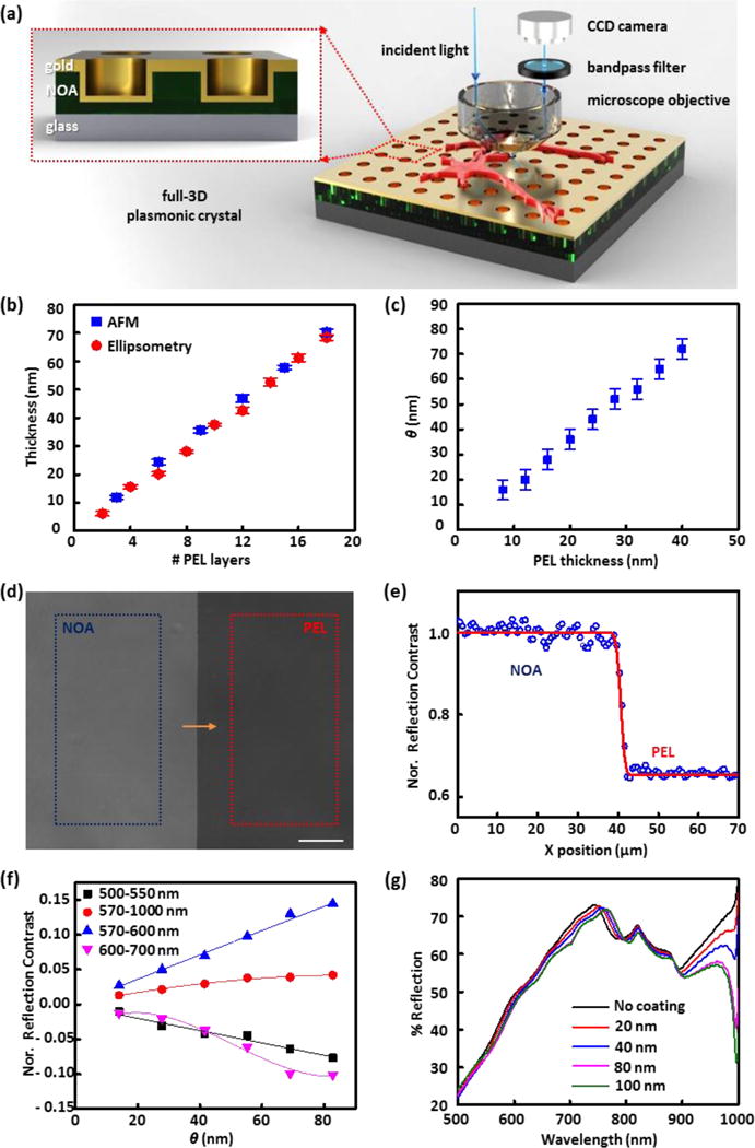
Figure 1.

(a) Schematic illustration of the plasmonic reflection imaging system setup with a laboratory microscope, bandpass filters, CCD camera, and a full 3D plasmonic crystal. (Inset) A close-up illustration of the cross-section of the full 3D plasmonic crystal. (b) Thickness values of polyelectrolyte assemblies measured at increasing numbers of polyelectrolyte layer (PEL) depositions using AFM and ellipsometry. (c) Corresponding pairs of thicknesses of polyelectrolyte films (n = 1.48) and index corrected mass coverages (θ) of live cells (n = 1.42). (d) Reflection image (using a 500–550 nm bandpass filter) of a polyelectrolyte layer-by-layer assembly (PEL) and photocured polyurethane film (NOA) on a plasmonic crystal used for reflection contrast calibration. Average pixel signal intensities were calculated in the regions marked with the blue (NOA region) and red box (PEL region), and used for reflection contrast calibration. The scale bar corresponds to 100 μm. (e) Step-edge profile of normalized reflection contrast (blue circles) along the yellow arrow in (d) and fitted red curve with a Gaussian width of 0.84 μm. (f) Normalized reflection contrast (NRC) as a function of index corrected thickness (θ) determined using different bandpass filters: 500–550 nm (black squares), 570–1000 nm (red circles), 570–600 nm (blue triangles), and 600–700 nm (pink inverted triangles). The error bars are obscured by the data markers themselves as a result of the large number of pixels (more than 30,000) used to determine the value. (g) FDTD calculated reflection spectra for varying thickness of index corrected material on a nanostructured plasmonic crystal.
