Abstract
Electrostatically actuated deformable mirrors with four concentric annular electrodes can exert independent control over defocus as well as primary, secondary, and tertiary spherical aberration. In this paper we use both numerical modeling and physical measurements to characterize recently developed deformable mirrors with respect to the amount of spherical aberration each can impart, and the dependence of that aberration control on the amount of defocus the mirror is providing. We find that a four-zone, 4 mm diameter mirror can generate surface shapes with arbitrary primary, secondary, and tertiary spherical aberration over ranges of ±0.4, ±0.2, and ±0.15 μm, respectively, referred to a non-normalized Zernike polynomial basis. We demonstrate the utility of this mirror for aberration-compensated focusing of a high NA optical system.
1. INTRODUCTION AND BACKGROUND
The demand for small-form-factor imaging systems continues to push the miniaturization limits of high-quality optics. Platforms necessitating small optics include cell phone cameras, machine vision, tablets, endoscopic microscopes and cameras, optical pick-ups, and pico-projectors. A key need for these imaging systems is focus control. The traditional mechanism of focusing by translating lenses is slow, and carries mechanical complexity, which can act as a barrier to miniaturization. As an alternative to translating lenses, investigators have explored variable-power optical elements that can be controlled electronically. Varifocus lenses have already been demonstrated in microscopy [1–5], ocular adaptive optics [6,7], cameras [8–11], astronomy [6,12,13], optical interconnects [14–16], pulse compression or shaping [17–19], optical data storage [20–23], micromachining [24,25], and optical tweezers [26]. Active optical elements include deformable membrane mirrors [9,27–33], liquid-filled lenses [34–41], and spatial light modulators [42–44]. Microelectromechanical systems (MEMS) comprise the majority of such elements due to relative ease of fabrication. Electromechanical actuation can be integrated with the optical device while maintaining precise dimensional control and the ability to incorporate a variety of optical materials.
Deformable MEMS mirrors are variable-power, reflective optical elements that have several compelling properties. A large adjustable wavefront sag of several tens of micrometers provides a useful range of optical power. For example, a 4 mm diameter mirror that can deliver a variable wavefront sag of 30 μm corresponds to a variable focus lens with an adjustable focal length from infinity to 67 mm, or, equivalently, a range of 15 diopters. In the case of electrostatically actuated mirrors, the number and arrangement of electrodes is flexible, allowing for adaptive surface shapes and a simple interface for control. Due to the low mass of a thin membrane, these elements can be quite fast (tens of kilohertz bandwidth) in comparison with alternative technologies. Additionally, reflective elements also possess the advantage of being achromatic.
Two main categories of deformable MEMS mirrors exist. The majority of MEMS mirrors on the market and investigated in academia primarily perform aberration correction with minimal defocus capability. An adaptive surface means these mirrors can dynamically adjust their aberration balance according to system demands. They often have a many-zone actuator scheme (often consisting of 35 or more surface zones) to allow for fine shape control [45]. Of these many-zone adaptive mirrors, some have sufficiently large stroke to perform significant defocus in addition to aberration correction. Our laboratory group [1,23,46,47] and Fanget et al. [21] have followed a different approach: employing a small number of concentric electrodes to induce large defocus while preserving the ability to balance system spherical aberration. This approach minimizes the complexity (especially interconnect cabling complexity for miniaturized systems) and overall cost of the active optical system. For narrow field imaging applications, such as in scanning confocal systems, performing defocus while concurrently managing attendant spherical aberration can sufficiently maintain high image quality. The mirrors described in this paper have four concentric electrodes that allow for up to 4 degrees of freedom, so defocus, primary, secondary, and tertiary spherical aberration may all be addressed.
In an effort to increase the total optical power range and deflection of MEMS focusing mirrors, our group and others have explored the use of polymer materials to reduce intrinsic stress of the membrane layer [1,9,29,30,48,49]. Previously, we reported a simple single silicon wafer process that utilizes the polymer SU-8 2002 as the membrane layer [1]. The surface-micromachining process uses an array of small vias in the membrane and xenon difluoride (XeF2) gas to etch the silicon below the membrane, which results in a non-uniform air gap underneath. To mitigate this issue, we recently developed a novel mirror design utilizing a single silicon-on-insulator (SOI) wafer [5]. The top “device” silicon is used as a sacrificial layer, and the buried oxide layer serves as a vertical etch stop to define a uniform air gap across the device.
This paper describes for the first time, to the best of our knowledge, a systematic characterization of this new style of four-zone deformable mirror, including an electromechanical model for predictive simulation and a training algorithm to determine electrode voltages to achieve a target optical prescription. We include experimental optical measurements of the full range of defocus as well as primary, secondary, and tertiary spherical aberration addressable by these devices that are designed for 0°, 5°, 10°, and 45° angles of incidence. Finally, a demonstration of aberration-balanced, active focusing through a 100 × 0.75 NA microscope objective with a mirror designed for 5° incidence angle illustrates the usefulness of these mirrors in an optical system.
2. MIRROR STRUCTURE
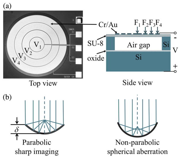
Our deformable mirror is illustrated in Fig. 1. A 2.5 μm thick membrane of SU-8 2002 is suspended over a large 40 μm air gap to allow for significant defocus [Fig. 1(a)]. Four concentric gold electrodes serve as the reflective mirror, and also provide electrostatic pressure to deform the membrane; controlling the voltage independently on these electrodes changes the spherical aberration balance of the mirror. For example, if the electrostatic force results in parabolic deflection of the mirror, then rays from a distant object form a sharp image [Fig. 1(b)]. If the result is a non-parabolic shape, then spherical aberration exists and the rays focus at different points along the optical axis, resulting in reduced image quality.
Fig. 1.
(a) Photograph of a released 4 mm diameter mirror with its four electrodes labeled. The resulting electrostatic force from the applied voltage is shown in the cross-section diagram. (b) Voltages resulting in the parabolic shape of the mirror allow for sharp imaging of infinite conjugate rays, while a non-parabolic shape leads to spherical aberration, where rays focus at different distances along the center axis. The total deflection, δ, represents the mirror sag of the reflective surface.
In this paper we describe circular deformable mirrors that are intended for focusing a beam that is incident normal to the mirror surface, and elliptical boundary mirrors that are designed for specific non-normal angles of incidence α2. For the elliptical mirrors, the ellipse major semi-axis, b, is related to the minor semi-axis, a, according to b = a/cos(α2) in order to eliminate primary astigmatism of the reflected beam [50].
A. MEMS Mirror Fabrication
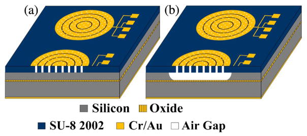
Figure 2 illustrates the fabrication process for the mirrors, which has been previously described in detail [5]. The thin SU-8 membrane is spin coated and photopatterned to create small 4 μm diameter etch vias. The metal layers (6 nm Cr under 160 nm Au) are subsequently evaporated and patterned to define the reflective electrode pattern on the top, and the electrical connection to the substrate on the back side [Fig. 2(a)]. The device is then released using a dry etch to isotropically remove the silicon under the membrane [Fig. 2(b)]. The simple process has greater than 80% device yield and results in high-optical-quality mirrors with less than 20 nm root-mean-square (rms) surface deviation when flat.
Fig. 2.
(a) Cross section of the unreleased mirror. (b) Free-standing membrane mirror after the release etch [5].
While the buried oxide layer serves as a vertical etch stop, these mirrors have no lateral etch stop. Because XeF2 etches isotropically, some overetching occurs in the radial direction, making the membrane physical diameter larger than the mirror diameter [Fig. 2(b)]. The term mirror sag refers to displacement of only the optical surface and not total displacement of the membrane. All mirrors have a minor diameter of 4 mm. Table 1 has the dimensions of the optical surfaces and the free-standing membrane of all of the mirrors tested. For instance, the 4 mm circular mirror has an optical surface that has a 4.000 mm diameter, whereas its free-standing membrane has a 4.352 mm diameter.
Table 1.
Comparison of the Dimensions of the Reflective Optical Surface and the Free-standing Membrane
| Incidence angle | Optical surface (mm) | Free-standing membrane (mm) |
|---|---|---|
| 0° | 4.000 | 4.352 |
| 5° | 4.000 × 4.015 | 4.420 × 4.435 |
| 10° | 4.000 × 4.062 | 4.392 × 4.454 |
| 45° | 4.000 × 5.657 | 4.328 × 5.985 |
B. Membrane Model
To predict the deflection and the range of possible surface shapes for our annular, four-zone mirror, we have created a simple electromechanical model of the device. The deformable mirror can be viewed as a circular or elliptical clamped plate with initial in-plane tension. Following the analysis by Sheplak and Dugundji [51], we compute the non-dimensional tension parameter , where a is the membrane radius and h is the thickness, ν is Poisson’s ratio, σ is the initial film stress, and E is the modulus of elasticity. For the 4 mm diameter circular mirrors (described in Section 2.A), nominal values are a = 2 mm, h = 2.5 μm, ν = 0.22, σ = 14.9 MPa, and E = 2 GPa, resulting in k = 234. Even allowing for a variation of a factor of 2 in the elastic modulus or in-plane stress values, our large k-value places the devices safely within the regime described by the simple linear membrane equation, for displacements of up to 10h = 25 μm. We therefore solve the membrane differential equation
| (1) |
where s is displacement, T = σh is the in-plane tension, and ρ is the area density. We are assuming static solutions, so the time derivative is zero. The applied electrostatic pressure p depends on the voltage and the separation between the electrode and the substrate, which, in turn, depends on local membrane displacement. The pressure may be represented as
| (2) |
where V (r) is the applied voltage, so is the starting air gap, εo is the permittivity of free space, and εr = 3.2 is the relative permittivity of the SU-8 2002 membrane material. The numerical solution is handled in MATLAB using the bvp4c ODE solver. The forcing pressure is computed for a constant voltage in each electrode zone, as illustrated in Fig. 1(a) above.
For quantitative analysis of the membrane shape, it is useful to fit the deflection curves as an expansion in terms of the circularly symmetric Zernike polynomials. The first four polynomials are listed in Table 2, which includes terms up to order 8 in the radial coordinate. Note that these are the un-normalized versions of the radial Zernike polynomials, which are orthogonal on the unit disk.
Table 2.
Zernike Modes: Orders, Frequencies, Respective Polynomials, and Aberration Typea
| Order (n) | Frequency (m) | Polynomial | Aberration type |
|---|---|---|---|
| 2 | 0 | 2ρ2 − l | Defocus |
| 4 | 0 | 6ρ4 − 6ρ2 + 1 | Primary spherical |
| 6 | 0 | 20ρ6 − 30ρ4 + 12ρ2 − 1 | Secondary spherical |
| 8 | 0 | 70ρ8 − 140ρ6 +90ρ4 − 20ρ2 + 1 |
Tertiary spherical |
The normalized pupil radius is ρ.
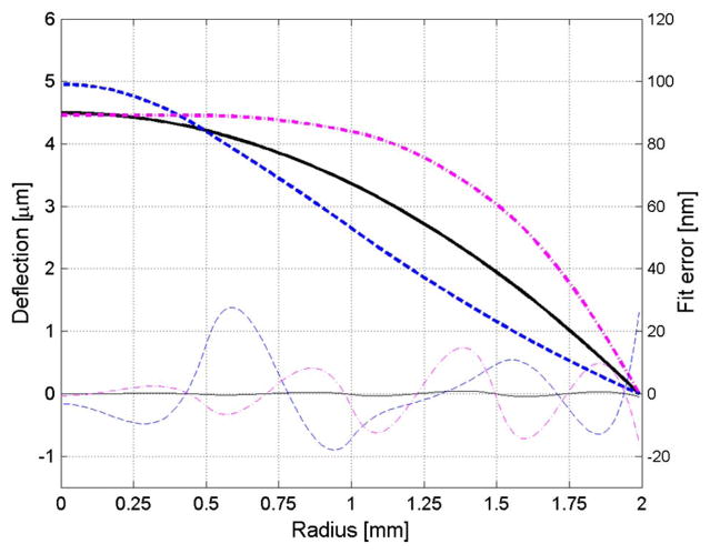
When actuating the mirror, the voltage profile cannot be chosen arbitrarily. The voltage difference between neighboring electrodes is limited to less than 120 V to prevent shorting between electrodes that are separated by gaps only 15 μm wide. We also limit absolute voltage delivered to any electrode to less than 400 V to prevent electrical breakdown through the SU-8 2002 film layer. However, within these constraints we find that a wide range of surface shapes are possible. Figure 3 illustrates three different deflection profiles (plotted as heavy lines in the figure) for a circular mirror that each exhibit the same amount of defocus, . The solid curve has minimal spherical aberration of all orders. The dashed curve, with no electrostatic pressure at the edge and maximum pressure at the center, exhibits positive primary spherical and negative secondary spherical . The dashed–dotted curve has minimal pressure at the center, increasing at the maximum rate radially. An overall voltage offset is adjusted to achieve the same . In this case, the primary spherical is negative with value , with a small amount of secondary spherical . The figure also plots the residual fit error between the simulated membrane shape and the best-fit four-term Zernike expansion. These are plotted using light lines, and with reference to the y axis on the right side of the figure. The worst-fit error for these three examples is for the dashed curve with positive primary spherical, but the error is only 11 nm rms. For the shapes reported in this paper, which are dominated by the defocus term, the quality of fit is excellent when limiting the curve fits to the first four Zernike polynomials. Other shapes are possible, however, that might require one or more additional Zernike radial modes to adequately describe the surface shape.
Fig. 3.
Three simulated surface profiles for a 4 mm diameter mirror with parameters corresponding to those of the fabricated devices. The y-axis scale on the left is for the mirror deflection s, plotted as heavy lines in the figure. The light lines show the error between the simulated shape and the best-fit Zernike expansion, plotted using the y-axis scale on the right. Solid curve: . Dashed curve: . Dashed–dotted curve: .
C. Mirror Calibration and Training
To use these mirrors for electronic focus control, appropriate control voltages must be selected to achieve a desired aberration balance. We describe here a mapping between zone voltages and resultant Zernike mode amplitudes that is convenient when system aberrations can be measured and quantified as a Zernike expansion, for example, when using a wavefront sensor (WFS). Other mappings are possible, such as mapping the voltage profile to the average zonal deflections, or mapping single electrodes to displacement “influence functions.” Because of the mirror structure and the nonlinearity of the system, the influence of all of the electrodes is highly coupled. In this paper we will use the Zernike mapping for its convenience when using a WFS for system optimization.
The pressure within any electrode zone depends nonlinearly on the zone voltage and the variable air gap under the membrane, according to Eq. (2). We assume, however, that the influence of the applied voltages on the resultant Zernike spectrum may be linearized over a sufficiently local region of Zernike space. Furthermore, we have demonstrated that the linear mapping applies to a larger region when we linearize using the square of the applied voltages. We therefore proceed as follows. A baseline voltage vector is applied to the mirror, and the resulting best-fit baseline Zernike vector is computed, based on the simulated or measured resultant membrane shape. A new voltage vector results in a Zernike vector . We assume a linear mapping:
where ΔZ = Z − Zb and , and V2 indicates a vector where each value is the square of the applied voltage for that zone. The 4 × 4 system matrix B is found as a least-squares best-fit from several trial shapes obtained in the vicinity of Vb and Zb.
To illustrate the procedure, we simulate the membrane using our numerical model. The physical parameters are chosen to correspond to a fabricated 4 mm diameter circular mirror, described in more detail below. We select an initial baseline voltage vector for which . The simulated baseline mirror shape produces . Next the mirror is simulated for perturbations of the control voltages in the vicinity of Vb. Systematically, each zone voltage is set to Vb, Vb − ΔV, and Vb + ΔV. We select ΔV = 60 V, so that neighboring voltage differences never exceed 2ΔV = 120 V. A total of 34 = 81 simulations results in a training matrix ΔV2 of dimension 4 × 81 and corresponding ΔZ with dimension 4 × 81. The least-squares best-fit system matrix B now provides a mapping between any desired Zernike vector, in a sufficiently close neighborhood to the baseline vector Zb, to the appropriate control voltage vector V to produce that shape.
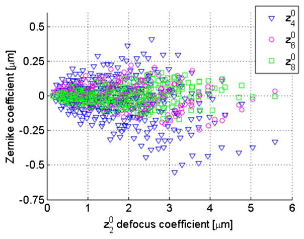
We reasonably expect this training procedure to be able to accurately produce Zernike terms only within the range of values used during the training. We studied our simulated mirror using four different baseline voltages of 125, 177, 217, and 240 V. A composite plot of the resulting Zernike coefficients determined from the 4 × 81 = 324 simulations is shown in Fig. 4. Here we plot the defocus term versus the primary, secondary, and tertiary spherical aberration terms, , and , respectively. As the mirror deflects with greater curvature, there is a greater range of control of the attendant spherical aberration components. Note that this plot represents the results using baseline voltage vectors with equal voltage on all four zones. The range of possible shapes illustrated by this figure does not capture the full range of spherical aberration control of which the four-zone mirror is capable. It does, however, illustrate a usefully large range of defocus and aberration values that can be addressed for aberration compensated focus control in a real system, as we will show in Section 4.
Fig. 4.
Aggregate plot of Zernike coefficients determined by 324 simulations, illustrating the range of aberration correction addressable as a function of the amount of defocus, . Primary spherical aberration coefficient values are plotted as triangles, secondary spherical as circles, and tertiary spherical as squares.
3. CHARACTERIZATION OF FABRICATED MIRRORS
This section includes static characterization of surface flatness at rest, voltage versus mirror sag, the measured range of spherical aberration control, and frequency response of these mirrors.
A. Static Characterization
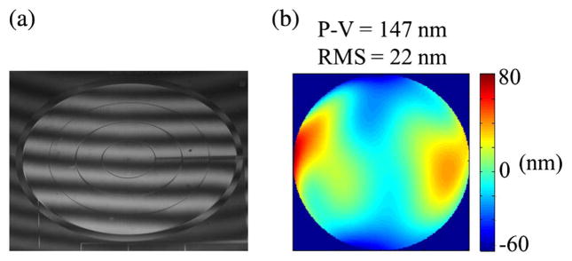
We use phase shift interferometry (λ = 850 nm) to measure the deflection of these mirrors [Fig. 5(a)]. The interferometric data is converted to a height map for the mirror surface, which is then analyzed by fitting to a full 55-term Zernike polynomial expansion up to the 9th order—n = 9. When analyzing elliptical mirrors, we first employ a coordinate transformation to generate a circular pupil before performing the Zernike fit. As an example, Fig. 5(b) plots the surface height of an unactuated 4 mm × 5.66 mm mirror after subtracting tilt and curvature terms, showing the height mapped onto a circular pupil. We observe that this mirror has a peak-to-valley deviation of 147 nm and a rms variation of 22 nm. Note that all mirror surface height data and Zernike coefficient data presented in this paper correspond to mirror deflection, s. The optical wavefront modulation W is related to the mirror surface deflection according to W = 2s cos(α2), where α2 is the incidence angle of the light beam on the mirror.
Fig. 5.
(a) Interferogram of the 4 mm × 5.66 mm mirror at rest, used to determine surface profile. (b) Corresponding surface profile. The peak-to-valley height variation is 147 nm and the rms surface deviation is 22 nm. Note that the interferometric data for all elliptical devices are first transformed to a circular coordinate system before applying Zernike fits and presenting the measured height profiles.
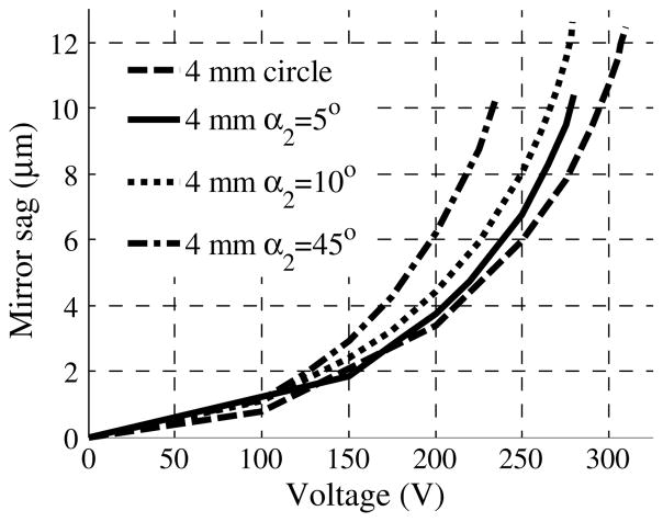
The focus control ability of these mirrors is directly related to the available deflection. Figure 6 shows the measured mirror sag as a function of voltage V, when the same voltage is applied to all four electrodes. Note that mirror sag, δ, is defined as the deflection of the center of the metalized mirror surface relative to its perimeter. Overall membrane deflection is slightly greater since the membrane boundary is larger than the mirror boundary, as discussed previously. As shown in Figure 6, mirror sags in excess of 10 μm are observed for all of the mirrors. By comparing measured deflection data to our numerical model described in Section 2.B, we determine the membrane tension, T, and calculate a 14.9 MPa intrinsic stress for the SU-8 2002 film.
Fig. 6.
Mirror sag as a function of voltage for four mirrors tested. The larger mirrors require less voltage for a given mirror sag.
B. Measured Range of Spherical Aberration
Following the procedure outlined in Section 2.C, we performed a full characterization of the four mirrors designed for four different angles of incidence: α2 = 0°, α2 = 5°, α2 = 10°, and α2 = 45°. Four baseline voltages were chosen that correspond with 2, 4, 6, and 8 μm of mirror sag. We trained using 81 different voltage profiles around each baseline vector to determine a local linear calibration matrix B. For each of the four mirrors, we plot the range of primary, secondary, and tertiary spherical aberration that was measured during training, where the results are indicative of the ability of the mirror to control these aberrations in an optical system.
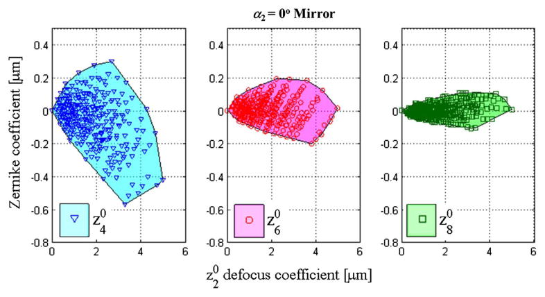
Figure 7 shows the results for a circular 4 mm diameter mirror for α2 = 0°. We observe from the plot a full range of primary spherical aberration from −0.57 to +0.30 μm. Measured ranged from −0.20 to +0.19 μm, and measured ranged from −0.11 to +0.11 μm. In comparing this figure to the simulation results of Fig. 4, we observe that the simulations and measurements are in good agreement.
Fig. 7.
Spherical aberration capability of a circular mirror.
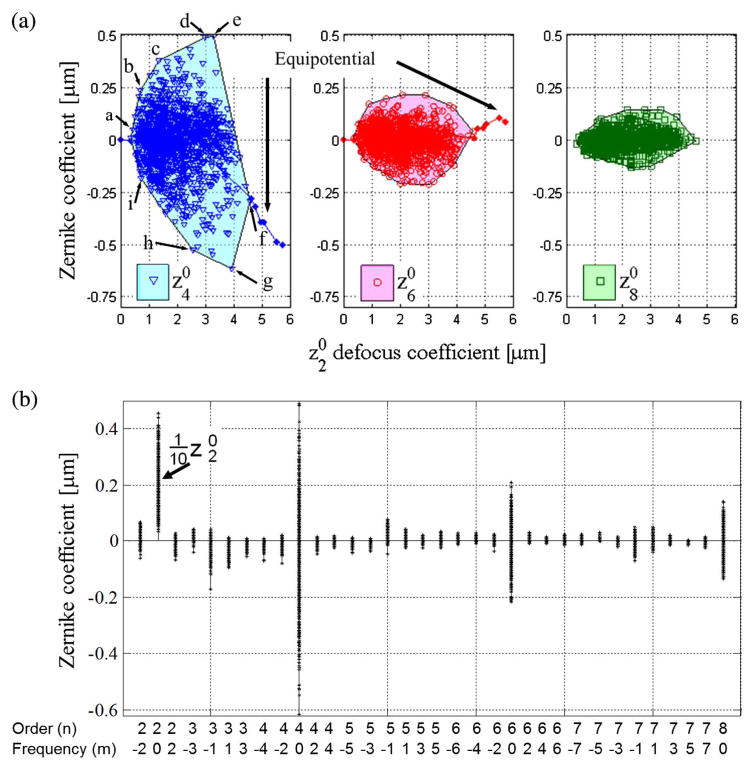
For the α2 = 5° mirror, additional voltage profiles were taken to better observe maximum and minimum primary spherical aberration capabilities [Fig. 8(a)]. For instance, where the 81 training voltage vectors had a maximum voltage differential of 120 V between any neighboring pair of the four electrodes, the additional voltage profiles allowed greater differential between non-neighboring electrodes. Table 3 provides the voltage profiles for the outer range of primary spherical aberration measurements shown in Fig. 8(a). For example, in the case of coordinate b, the difference between the voltage potential on the innermost electrode to the outermost electrode is 225.5 V − 49.7 V = 175.8 V. Neighboring electrode potentials still do not exceed 120 V to prevent arcing. We observe from the plot a full range of primary spherical aberration from −0.61 to 0.49 μm, measured ranged from −0.22 to 0.21 μm, and measured ranged from −0.13 to 0.14 μm. Figure 8(a) also has solid lines for the and values associated with equipotential voltages. The reduction in air gap distance at the center of the membrane with greater deflections causes negative primary spherical aberration, appearing as a more conical shape of the membrane for greater defocus values. A more bowl-like shape indicates positive primary spherical aberration. Secondary spherical aberration increases with greater equipotential deflection. The secondary spherical aberration polynomial has the opposite sign at the center of the pupil compared to the primary, so its influence is in agreement with that of primary spherical aberration in describing the conical shape at greater deflections.
Fig. 8.
(a) Spherical aberration capability of α2 = 5° mirror with ±60 V test matrix performed at four deflections, and with additional ranges of voltages applied to determine maximum range. The algorithm was limited to a minimum of −255 V to prevent accidental snapdown. The blue and red solid lines with large markers show and Zernike coefficients with equipotential voltage on the mirror surface, respectively. (b) Composite Zernike spectra from the 827 measurements plotted in (a), showing aberrations from 2nd to 7th order and tertiary spherical.
Table 3.
Specific Voltages for the Outer Range of Values as Labeled in Fig. 8(a)
| Coordinate | V1 (V) | V2 (V) | V3 (V) | V4 (V) |
|---|---|---|---|---|
| a | 95.0 | 95.0 | 95.0 | 95.0 |
| b | 49.7 | 94.2 | 155.4 | 225.5 |
| c | 76.7 | 82.6 | 160.8 | 241.9 |
| d | 110.2 | 135.8 | 242.6 | 241.3 |
| e | 123.8 | 147.3 | 255.0 | 255.0 |
| f | 255.0 | 255.0 | 255.0 | 255.0 |
| g | 245.9 | 224.6 | 179.4 | 80.5 |
| h | 255.0 | 255.0 | 135.0 | 135.0 |
| i | 218.0 | 98.8 | 96.2 | 52.7 |
Figure 8(b) shows a composite of full Zernike spectra for 827 sample points for the 5° incidence angle mirror. The non-spherical aberration terms are generally below 50 nm, with many never exceeding 20 nm. The largest are astigmatism ( ) and coma, with coma ( ) reaching a maximum of −170 nm. Similar measurements of a circular mirror designed for normal incidence showed the largest mode amplitude (excluding spherical aberration) of 65 nm for .
A possible source of asymmetrical excitation is the electrode traces, which extend onto the mirror in one location [Fig. 1(a)], thus creating a single radial location with a unique feature. To determine if the electrode traces contributed to aberration terms with a cos(θ) or sin(θ) dependence (mode frequency m = ±1), we studied the correlation between and the terms , keeping the average membrane displacement nearly constant ( ). The term exhibited the strongest correlation, with , (R2 = 0.45). This is not a strong correlation, but it does indicate that adjusting spherical aberration can introduce a small amount of coma on the mirror. For the range plotted in Fig. 8, the resultant correlated coma would fall in the range of .
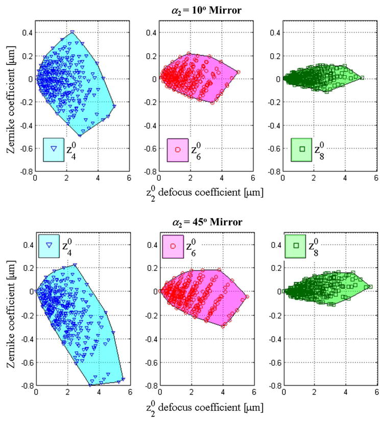
Figure 9 shows the spherical aberration capability of a 10° and 45° incidence angle mirror. The 45° mirror altered , and from −0.80 to 0.22 μm, −0.30 to 0.18 μm, and −0.11 to 0.16 μm, respectively. The larger membrane size results in less positive primary spherical aberration correction capability, while allowing greater magnitude of negative .
Fig. 9.
Spherical aberration capability of 10° and 45° mirrors with ±60 V test matrix performed at four deflections for each mirror.
C. Mirror Bandwidth for Dynamic Focus Control
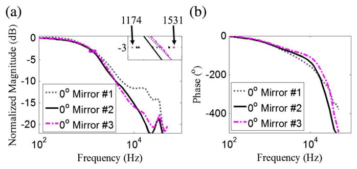
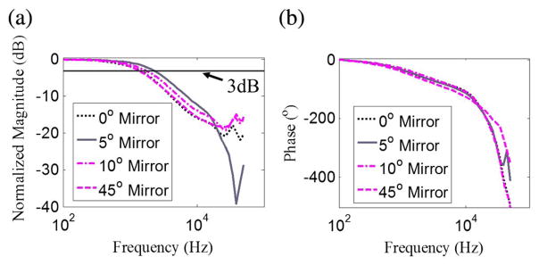
We measured the frequency response of the mirrors using a dc voltage with a small, superimposed sinusoidal driving voltage at the test frequency. A 633 nm collimated laser beam was reflected off of the mirror at a small angle, and the light intensity through a pinhole near focus was measured to determine the magnitude and phase of the mirror defocus response. Three circular mirrors exhibited similar dynamic performance (Fig. 10). Three to four trials for each mirror showed some variability, as shown in the top right corner of Fig. 10(a). By averaging the mean values of the three individual circular mirrors, the 3 dB magnitude is 1373 ± 60.5 Hz. The 90° phase lag occurs at a frequency similar to the 3 dB frequency. Figure 11 shows Bode plots for the off-axis mirrors. The average of 3 dB magnitudes measured from three trials on each mirror are 2283 ± 15 Hz, 1816 ± 70 Hz, and 1324 ± 54 Hz for the 5°, 10°, and 45° mirrors, respectively. While larger diameter and lower stress devices have the lowest resonant frequencies, the measured frequency response is dominated by air damping with 3 dB frequencies 1 order of magnitude lower than the first drumhead resonance. We have not attempted to model the air damping for these different mirror shapes. We note that the 3 dB frequency does not scale monotonically with mirror size, and is quite different for the 0° mirror and the 5° mirror, which are nearly identical in size. The frequency response for these mirrors is determined primarily by air damping, which is dependent on air flow through the small etch vias. The areal density of the via openings varies from mirror to mirror, from 1.7% to 2.3% of surface area. This is a difference of 35% in cross-sectional area that is open for air flow, and we attribute the variation in measured 3 dB frequency primarily to this variation.
Fig. 10.
(a) Normalized magnitude plot of three different 0° mirrors that were fabricated on the same wafer and under the same conditions. Three to four trials were done for each mirror and the 3 dB magnitude response for each of these trials are included in the top right corner. (b) Phase response for the three different 0° mirrors.
Fig. 11.
(a) Normalized magnitude plot of the four mirrors designed for various angles of incidence. (b) Phase response for the four mirrors.
4. FOCUS CONTROL DEMONSTRATION
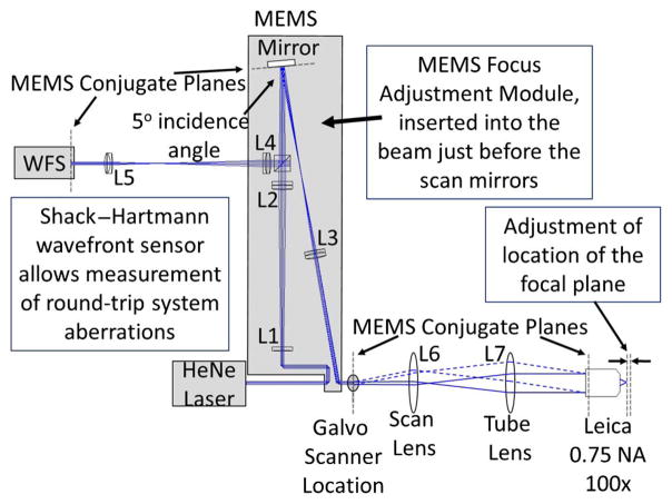
To demonstrate the usefulness of these mirrors, we show aberration-balanced, active focusing through a 100 ×, 0.75 NA microscope objective. This is achieved by inserting a MEMS focus adjustment module (MFAM) into the optical train of a benchtop system to evaluate performance for laser scanning microscopy (Fig. 12). The MFAM has a 4 mm diameter mirror designed for α2 = 5° incidence angle. Two fixed lenses (L1 and L2) in the MFAM expand the He–Ne laser beam to fill the MEMS mirror aperture, while lens L3 images the MEMS mirror at 7/8ths magnification at the galvo scanner location. The system is designed to deliver collimated light rays at the galvo scanner location (and at the objective lens) when the mirror has a 9 μm sag. This is within the full-range deflection of the MEMS mirror. A 10%/90% beam splitter samples the back-reflected beam, and two relay lenses (L4 and L5) image the MEMS mirror onto a WFS for measurement of round-trip aberration of the optical system. A scan lens, L6, and tube lens, L7, serve as a 1:1 relay between the galvo scanner location and the objective lens. The objective lens has a 3 mm diameter back aperture.
Fig. 12.
MFAM inserted into the optical train of a benchtop representation of a scanning laser microscope.
To assess the ability of the mirror to focus the system while compensating for spherical aberration, a flat optical mirror was placed at the focal plane behind the Leica objective lens and the wavefront was measured on the WFS. This location for the WFS will measure round-trip accumulated wavefront error corresponding to two passes through the objective lens, the relay lenses between the MEMS mirror and the objective lens, and two reflections from the MEMS mirror itself. Because spherical aberration has axial symmetry, the double pass through the optics will accumulate approximately twice the forward path aberration. We follow a training process similar to Section 2.C, obtaining training matrices at several focus positions (the baseline was a constant voltage on all electrodes), and solving for the local linear mapping B between the differential Zernike amplitudes ΔZ and the differential squared voltage ΔV2. After training, we attempted to find control voltages for each focus position that would minimize spherical aberration at that point.
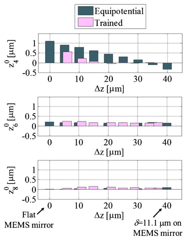
Our first attempts to use the linear mapping B to find control voltages that would drive all four Zernike terms ( , and ) to zero resulted in voltage profiles that were out of range (greater than 120 V between neighboring electrodes, or in excess of 400 V total, as discussed in Section 2.B). Therefore, we adopted a strategy that would minimize the dominant aberration, which was primary spherical , and left , and unchanged. This was successful in generating control voltages that were within the imposed voltage constraints. The results are plotted in Fig. 13. The top chart shows round-trip wavefront primary spherical aberration at the WFS. The green bars are the measured values for equal voltage on all four MEMS mirror electrodes (the baseline setting before training). The pink bars are the result after training to try to minimize .
Fig. 13.
Spherical aberration Zernike coefficients before training with equipotential voltages across all four electrodes and after training with optimized voltages applied to the MEMS mirror over a 40 μm focus range, Δz, behind the objective lens. The algorithm was able to correct over most of the focal range of the MEMS mirror.
Notice that increasing mirror deflection corresponds to moving to the right across the graph. Focus positions that cannot be fully corrected are those for which the mirror has very little baseline deflection. These positions also have the most uncorrected , indicated in the graph as a shift in the axial position of the pink bar with respect to the green one (the actual position of best focus is shifted from the baseline location associated with training). For a controlled focus range from 15 μm up to the maximum characterized displacement of 40 μm, was effectively nulled. The middle graph of Fig. 13 shows secondary spherical aberration, , which we attempted to hold constant before and after training. This was largely achieved throughout the focus range. The bottom graph plots tertiary spherical aberration, , which increased slightly after training. However, these values are small enough to be contributing minimally to the overall wavefront error.
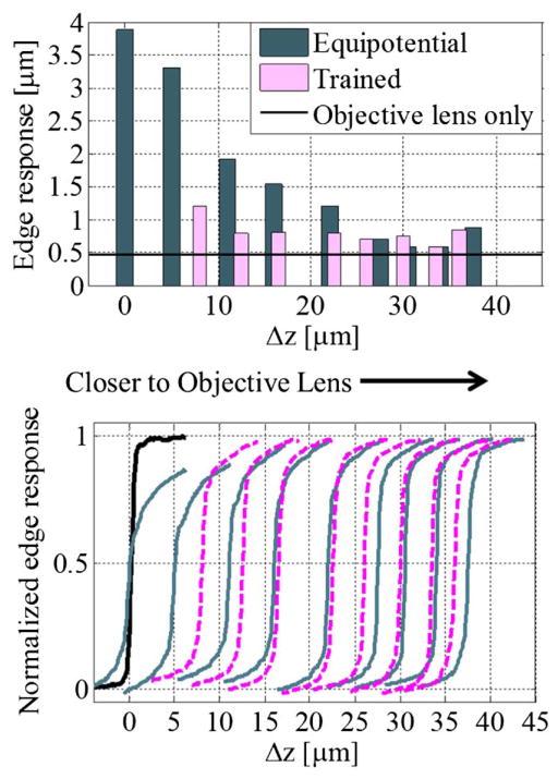
To further confirm aberration minimization using the MEMS mirror, we performed knife-edge measurements of the focused spot. These measurements were made in transmission at the location of best focus behind the objective lens. The results are shown in Fig. 14, where the actual edge response curves are plotted below, and the 20%–80% edge width versus focus position are plotted above. In most cases, the edge response after training was sharper than the measurement made with the constant voltage baseline deflection. For reference, we also measured the edge response of the objective lens with only a collimated beam, and without the MFAM optics. That edge response, with a 20%–80% width of 0.47 μm, is included in the plots for comparison. Over most of the focus adjustment range, the recovered edge response is within 0.3 μm of this value.
Fig. 14.
Knife-edge measurements corresponding to the WFS measurements shown in Fig. 13. Raw data is shown on the bottom. The MEMS mirror begins flat at Δz = 0 μm and has greater mirror sag as Δz increases in value. The entire optical system was removed for testing of the knife-edge response of the objective lens only (plotted using the heavy line at the Δz = 0 position).
5. SUMMARY AND CONCLUSIONS
We have shown that circular and elliptical deformable mirrors with four independent annular electrodes can adopt concave shapes for focus control that include a controllable amount of primary, secondary, and tertiary spherical aberration. Through both numerical simulation and experimental measurements, we characterized the range of spherical aberration correction that is possible for several 4 mm diameter MEMS mirrors, including elliptical mirrors designed for nonzero beam incidence angles. These mirrors had an air gap of 40 μm, with a maximum sag before snapdown of about 15 μm. We observe that some initial deflection of the mirror is necessary to control the aberrations. This results because the electrostatic force is only attractive, so any actuation of the mirror results in a mixture of defocus and spherical aberration. Furthermore, the results presented are specific for the mirror parameters as tested, and reflect a restriction to keep electrode-to-electrode voltage differentials less than 120 V, and overall voltage less than 255 V. With a larger gap between electrodes (to prevent interelectrode shorting), the mirrors might tolerate larger differential voltages, resulting in an even greater range of aberration correction. Nevertheless, from Fig. 8 we see that a defocus of only (mirror sag of approximately 2 μm) is sufficient for the mirror to be capable of controlling primary spherical within the range of , and with , the range for increases to more than ±0.4 μm. These are surface height values, so the optical wavefront correction is nearly twice this amount (assuming, for this example, a 5° beam incidence angle). Similarly, with that same defocus of , the higher order spherical aberration ranges are ±0.2 μm for and ±0.15 μm for (also from Fig. 8 data).
Through our simulations, which are confirmed with our experimental characterization, we showed that we can use a locally linear mapping between small changes in the four element Zernike vector with small changes in the four element squared voltage vector. A training algorithm that found a least-squares best-fit using this model was useful for finding appropriate control voltages to drive the mirror surface to a desired shape, provided that shape was reasonably close to the shapes used for training. Finally, we showed the utility of these four-zone mirrors and the training algorithm to achieve aberration-compensated focusing over a range of more than 40 μm in a benchtop microscope with NA = 0.75. We believe that this new class of mirrors can provide a powerful means to electronically control both focus and spherical aberration balance in high-performance, high-NA systems such as scanning confocal microscopes.
Acknowledgments
Funding. National Science Foundation (NSF) (0754608, 0956910, 1338133); National Institutes of Health (NIH) (1R21EB018507-01).
The MEMS mirrors were fabricated in the Montana Microfabrication Facility and the Lurie Nanofabrication Facility. The authors acknowledge the contributions of Krishna Chattergoon for his assistance with dynamic characterization of the MEMS mirrors and thank the reviewers for their helpful suggestions.
Footnotes
OCIS codes: (110.1080) Active or adaptive optics; (230.4685) Optical microelectromechanical devices; (220.1000) Aberration compensation; (230.4040) Mirrors; (110.0180) Microscopy.
References
- 1.Lukes SJ, Dickensheets DL. SU-8 2002 surface micromachined deformable membrane mirrors. J Microelectromech Syst. 2013;22:94–106. [Google Scholar]
- 2.Lutzenberger BJ, Moghimi MJ, Lukes SJ, Kaylor B, Dickensheets DL. MEMS deformable mirrors for focus control in vital microscopy. Proc SPIE. 2010;7594:759406. [Google Scholar]
- 3.Kang D, Yoo H, Jillella P, Bouma BE, Tearney GJ. Comprehensive volumetric confocal microscopy with adaptive focusing. Biomed Opt Express. 2011;2:1412–1422. doi: 10.1364/BOE.2.001412. [DOI] [PMC free article] [PubMed] [Google Scholar]
- 4.Tsai PS, Migliori B, Campbell K, Kim TN, Kam Z, Groisman A, Kleinfeld D. Spherical aberration correction in nonlinear microscopy and optical ablation using a transparent deformable membrane. Appl Phys Lett. 2007;91:191102. [Google Scholar]
- 5.Lukes SJ, Dickensheets DL. Agile scanning using a MEMS focus control mirror in a commercial confocal microscope. Proc SPIE. 2014;8949:89490W. [Google Scholar]
- 6.Devaney N, Dalimier E, Farrell T, Coburn D, Mackey R, Mackey D, Laurent F, Daly E, Dainty C. Correction of ocular and atmospheric wavefronts: a comparison of the performance of various deformable mirrors. Appl Opt. 2008;47:6550–6562. doi: 10.1364/ao.47.006550. [DOI] [PubMed] [Google Scholar]
- 7.Tuohy S, Bradu A, Podoleanu AG, Chateau N. Correcting ocular aberrations with a high stroke deformable mirror. Proc SPIE. 2007;6627:66271L. [Google Scholar]
- 8.Dickensheets DL, Moghimi MJ, Lukes SJ, Lutzenberger BJ, Kaylor BM, Schoessler J, Roos PA. A compact F/5 camera lens with MEMS focus control. International Conference on Mechanical Engineering; 2011. [Google Scholar]
- 9.Hsieh HT, Wei HC, Lin MH, Hsu WY, Cheng YC, Su GDJ. Thin autofocus camera module by a large-stroke micromachined deformable mirror. Opt Express. 2010;18:11097–11104. doi: 10.1364/OE.18.011097. [DOI] [PubMed] [Google Scholar]
- 10.Kuiper S, Hendriks BHW. Variable-focus liquid lens for miniature cameras. Appl Phys Lett. 2004;85:1128–1130. [Google Scholar]
- 11.Wang JL, Chen TY, Chien YH, Su GDJ. Miniature optical autofocus camera by micromachined fluoropolymer deformable mirror. Opt Express. 2009;17:6268–6274. doi: 10.1364/oe.17.006268. [DOI] [PubMed] [Google Scholar]
- 12.Zhao X, Xie Y, Zhao W. Broadband and wide field of view foveated imaging system in space. Opt Eng. 2008;47:103202. [Google Scholar]
- 13.Park JH, Garipov GK, Jeon JA, Khrenov BA, Kim JE, Kim M, Kim YK, Lee CH, Lee J, Na GW, Nam S, Park IH, Park YS. Obscura telescope with a MEMS micromirror array for space observation of transient luminous phenomena or fast-moving objects. Opt Express. 2008;16:20249–20257. doi: 10.1364/oe.16.020249. [DOI] [PubMed] [Google Scholar]
- 14.Peter YA, Gonte F, Herzig HP, Dandliker R. Micro-optical fiber switch for a large number of interconnects using a deformable mirror. IEEE Photon Technol Lett. 2002;14:301–303. [Google Scholar]
- 15.Xiaohua M, Kuo GS. Optical switching technology comparison: optical MEMS vs. other technologies. IEEE Commun Mag. 2003;41(11):50–57. [Google Scholar]
- 16.Chu PB, Brener I, Pu C, Lee SS, Dadap JI, Park S, Bergman K, Bonadeo NH, Chau T, Chou M, Doran RA, Gibson R, Harel R, Johnson JJ, Lee CD, Peale DR, Tang B, Tong DTK, Tsai MJ, Wu Q, Zhong W, Goldstein EL, Lin LY, Walker JA. Design and nonlinear servo control of MEMS mirrors and their performance in a large port-count optical switch. J Microelectromech Syst. 2005;14:261–273. [Google Scholar]
- 17.Bonora S, Brida D, Villoresi P, Cerullo G. Ultrabroadband pulse shaping with a push-pull deformable mirror. Opt Express. 2010;18:23147–23152. doi: 10.1364/OE.18.023147. [DOI] [PubMed] [Google Scholar]
- 18.Bonora S, Bortolozzo U, Naletto G, Residori S. Innovative membrane deformable mirrors. In: Tyson B, editor. Topics in Adaptive Optics. InTech; 2012. available from: http://www.intechopen.com/books/topics-in-adaptive-optics/innovative-membrane-deformable-mirrors. [Google Scholar]
- 19.Rondi A, Extermann J, Bonacina L, Weber SM, Wolf JP. Characterization of a MEMS-based pulse-shaping device in the deep ultraviolet. Appl Phys B. 2009;96:757–761. [Google Scholar]
- 20.Cheng X, Ma J, Hao Q. Dynamic focus control of the Blu-ray optical pickup unit. Proc SPIE. 2008;7100:71000V. [Google Scholar]
- 21.Fanget S, Labeye PR, Divoux C, Hugon X. Integrated deformable mirror on silicon for optical data storage. Proc SPIE. 2005;5721:159–169. [Google Scholar]
- 22.Aoki S, Yamada M, Yamagami T. A novel deformable mirror for spherical aberration compensation. Jpn J Appl Phys. 2009;48:03A003. [Google Scholar]
- 23.Lukes SJ, Dickensheets DL. MEMS focus control and spherical aberration correction for multilayer optical discs. Proc SPIE. 2012;8252:82520L. [Google Scholar]
- 24.Beck RJ, Parry JP, MacPherson WN, Waddie A, Weston NJ, Shephard JD, Hand DP. Application of cooled spatial light modulator for high power nanosecond laser micromachining. Opt Express. 2010;18:17059–17065. doi: 10.1364/OE.18.017059. [DOI] [PubMed] [Google Scholar]
- 25.Schwertner M, Booth MJ, Wilson T. Adaptive optics for microscopy, optical data storage, and micromachining. Proc SPIE. 2006;6306:63060A. [Google Scholar]
- 26.Huang Y, Wan J, Cheng MC, Zhang Z, Jhiang SM, Menq CH. Three-axis rapid steering of optically propelled micro/nanoparticles. Rev Sci Instrum. 2009;80:063107. doi: 10.1063/1.3156838. [DOI] [PubMed] [Google Scholar]
- 27.Lukes SJ, Dickensheets DL. SU-8 focus control mirrors released by XeF2 dry etch. Proc SPIE. 2011;7930:793006. [Google Scholar]
- 28.Korde UA. Large-displacement closed-loop control of variable area electrostatic actuation for membrane reflectors. J Intell Mater Syst Struct. 2009;20:697–721. [Google Scholar]
- 29.Lin MJ, Wu KW. Design and fabrication of an electrostatically actuated microdeformable focusing mirror. J Micro/Nanolithogr MEMS MOEMS. 2011;10:011504. [Google Scholar]
- 30.Wei HC, Su GDJ. A low voltage deformable mirror using ionic-polymer metal composite. Proc SPIE. 2010;7788:77880C. [Google Scholar]
- 31.Bonora S, Coburn D, Bortolozzo U, Dainty C, Residori S. High resolution wavefront correction with photocontrolled deformable mirror. Opt Express. 2012;20:5178–5188. doi: 10.1364/OE.20.005178. [DOI] [PubMed] [Google Scholar]
- 32.Lin PY, Hsieh HT, Su GDJ. Design and fabrication of a large-stroke MEMS deformable mirror for wavefront control. J Opt. 2011;13:055404. [Google Scholar]
- 33.Moghimi MJ, Chattergoon KN, Wilson CR, Dickensheets DL. High speed focus control MEMS mirror with controlled air damping for vital microscopy. J Microelectromech Syst. 2013;22:938–948. [Google Scholar]
- 34.Berge B. Liquid lens technology: principle of electrowetting based lenses and applications to imaging. IEEE International Conference on MEMS; 2005; pp. 227–230. [Google Scholar]
- 35.Cu-Nguyen PH, Seifert A, Zappe H. Tunable hyperchromatic microlens array for compact 2D spectrometry. Microoptics Conference; IEEE; 2015. [Google Scholar]
- 36.Yang H, Yang CY, Yeh MS. Miniaturized variable-focus lens fabrication using liquid filling technique. Microsyst Technol. 2008;14:1067–1072. [Google Scholar]
- 37.Lee SW, Lee SS. Focal tunable liquid lens integrated with an electromagnetic actuator. Appl Phys Lett. 2007;90:121129. [Google Scholar]
- 38.Hendriks BHW, Kuiper S, Van As MAJ, Renders CA, Tukker TW. Electrowetting-based variable-focus lens for miniature systems. Opt Rev. 2005;12:255–259. [Google Scholar]
- 39.Carpi F, Frediani G, Turco S, De Rossi D. Bioinspired tunable lens with muscle-like electroactive elastomers. Adv Funct Mater. 2011;21:4152–4158. [Google Scholar]
- 40.Dubois P, Rosset S, Koster S, Stauffer J, Mikhaïlov S, Dadras M, Rooij NFD, Shea H. Microactuators based on ion implanted dielectric electroactive polymer (EAP) membranes. Sens Actuators A. 2006;130–131:147–154. [Google Scholar]
- 41.Zhao P, Ataman Ç, Zappe H. Spherical aberration free liquid-filled tunable lens with variable thickness membrane. Opt Express. 2015;23:21264–21278. doi: 10.1364/OE.23.021264. [DOI] [PubMed] [Google Scholar]
- 42.Martinez T, Wick DV, Payne DM, Baker JT, Restaino SR. Non-mechanical zoom system. Proc SPIE. 2004;5234:375–378. [Google Scholar]
- 43.Wick DV, Bagwell BE, Sweatt WC, Peterson GL, Martinez T, Restaino SR, Andrews JR, Wilcox CC, Payne DM, Romeo R. Active optical zoom for space-based imaging. Proc SPIE. 2006;6307:63070A. [Google Scholar]
- 44.Stockbridge C, Lu Y, Moore J, Hoffman S, Paxman R, Toussaint K, Bifano T. Focusing through dynamic scattering media. Opt Express. 2012;20:15086–15092. doi: 10.1364/OE.20.015086. [DOI] [PubMed] [Google Scholar]
- 45.Loktev M, De Lima Monteiro DW, Vdovin G. Comparison study of the performance of piston, thin plate and membrane mirrors for correction of turbulence-induced phase distortions. Opt Commun. 2001;192:91–99. [Google Scholar]
- 46.Himiner P, Dickensheets D. High speed, large deflection deformable mirrors for focus and spherical aberration control. IEEE/LEOS International Conference on Optical MEMs; 2002; pp. 193–194. [Google Scholar]
- 47.Dickensheets DL, Ashcraft PV, Himmer PA. Pixel-by-pixel aberration correction for scanned-beam micro-optical instruments. Proc SPIE. 1999;3878:48–57. [Google Scholar]
- 48.Friese C, Wissmann M, Zappe H. Polymer-based membrane mirrors for micro-optical sensors. Proceedings of IEEE Sensors 1. 2003:667–672. [Google Scholar]
- 49.Oliver KW, Lukes SJ, Moghimi MJ, Dickensheets DL. Stress engineering for free-standing SU-8 2002 thin film devices. Proc SPIE. 2012;8248:82480H. [Google Scholar]
- 50.Lukes SJ. PhD dissertation. Montana State University; 2015. Imaging performance of elliptical-boundary varifocal mirrors in active optical systems. [Google Scholar]
- 51.Sheplak M, Dugundji J. Large deflections of clamped circular plates under initial tension and transitions to membrane behavior. J Appl Mech. 1998;65:107–115. [Google Scholar]


