Abstract
Recent studies of single-molecule thermoelectricity have identified families of high-performance molecules. However, in order to translate this discovery into practical thin-film energy-harvesting devices, there is a need for an understanding of the fundamental issues arising when such junctions are placed in parallel. This is relevant because controlled scalability might be used to boost electrical and thermoelectric performance over the current single-junction paradigm. As a first step in this direction, we investigate here the properties of two C60 molecules placed in parallel and sandwiched between top and bottom graphene electrodes. In contrast with classical conductors, we find that increasing the number of parallel junctions from one to two can cause the electrical conductance to increase by more than a factor of 2. Furthermore, we show that the Seebeck coefficient is sensitive to the number of parallel molecules sandwiched between the electrodes, whereas classically it should be unchanged. This non-classical behaviour of the electrical conductance and Seebeck coefficient are due to inter-junction quantum interference, mediated by the electrodes, which leads to an enhanced response in these vertical molecular devices.
Introduction
Molecular devices consisting of single or multiple molecules bridging two or more electrodes have attracted intense theoretical and experimental interest, due to their tuneable and unique transport properties, including negative differential resistance (NDR)1–3 electrical switching4–6 and thermoelectric power generation7–13. The conversion of a temperature gradient ΔT to a voltage difference ΔV is controlled by the Seebeck coefficient S = −ΔV/ΔT. Common inorganic thermoelectric materials such as Pb, Bi, Co, Sb are toxic and expensive due to limited global sources. Therefore, in recent years, different strategies have been proposed to exploit the thermoelectric properties of nanostructured organic materials or organic molecules14–18. At the single-molecule level, the Seebeck coefficient S can be controlled using a gate electrode in a three-terminal device19. Furthermore, the sign and magnitude of S can be changed by modulating the coupling of the molecule to electrodes using the pressure induced by a STM tip9. Additionally, it has been demonstrated that the Seebeck coefficient of molecular junctions can be enhanced by manipulating the intermolecular interactions of C60 molecules placed in series between two gold electrodes10. This effect arises from the quantum mechanical origin of thermopower at the molecular scale. Indeed at a qualitative level, if the transmission probability of electrons with energy E passing from one electrode to another through a C60 molecule is T 1(E), the transmission probability through two C60 molecules placed in series is approximately proportional to T 1(E)2. Consequently, (after averaging over a quantum phase) the conductance of two molecules placed in series G 2 is equal to , whereas Ohm’s law predicts G 2 = G 1/2. Similarly, the Mott formula , predicts that the thermopower coefficients are related by , whereas classically S 2 should be the same with S 1. The aim of the present paper is to determine if similar non-classical behaviour occurs when molecules are placed in parallel between two electrodes as in the concept device shown in Fig. 1(a). If two such molecules in parallel behave classically, then the electrical conductance doubles according to Ohm’s law and the Seebeck coefficient is unchanged. Consequently, if many molecules were placed in parallel to form a self-assembled monolayer (SAM), then the electrical conductance would be proportional to the number of molecules and the Seebeck coefficient would be insensitive to the number of parallel molecules bridging the junction. Reuter and co-workers have addressed how the electrical conductance of two molecules placed in parallel between two electrodes need not be 2G 1, and have proposed that deviations from Ohm’s law are a signature of direct inter-molecular interactions or ‘cooperativity’20. In what follows, our aim is to examine this expectation from a microscopic point of view by computing the change in thermoelectric properties when two C60 molecules are placed in parallel between two graphene electrodes. Our results demonstrate that even when there is no direct inter-molecular coupling, indirect inter-molecular interactions mediated by the graphene electrodes produce quantum interference effects in the electronic structure of the molecular junction. As a consequence, the Seebeck coefficient is sensitive to the number N of parallel molecules and the electrical conductance is not simply proportional to N. These indirect interactions, if controlled properly can boost the electrical and thermoelectric performance of a device over the single-molecule paradigm.
Figure 1.
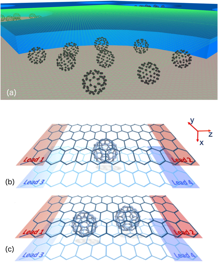
(a) Vertical scalable concept for molecular thermoelectricity. An insulating spacer is placed on top of a graphene bottom electrode, and drilled with nanopores. These pores are filled with C60 molecules. A top graphene electrode is deposited. Thermoelectricity is enhanced by Quantum Interference. Schematics of the two simulated devices: (b) a C60-monomer and (c) a C60-dimer sandwiched between two graphene monolayers.
Results
We have designed the vertical four-terminal devices shown in Fig. 1(b) and (c), where a single C60 and a C60 dimer are sandwiched between two horizontal graphene sheets, respectively. The two graphene sheets are separated by an optimized vertical distance and are electronically decoupled, except via the transport path though the buckyball(s) from the top to the lower sheet. The transmission functions T 1,2(E) for electrons of energy E passing from the top-left electrode (lead 1) to the bottom-right electrode (lead 4) are shown in Fig. 2 for the C60-monomer and -dimer devices21. As expected, due to the periodic boundary conditions chosen for the electrodes, the number of open channels for both devices is 2 in the energy range between −1.5 and +1.5 eV around the Fermi energy E F. The energy position of the HOMO- and LUMO-mediated (highest-occupied and lowest unoccupied molecular orbital, respectively) resonances does not depend on the relative position and orientation of the molecule and the graphene electrodes for van der Waals chemical bonding22. We therefore predict that T 1,2(E) in Fig. 2 should remain qualitatively the same as the C60 molecules move around and rotate. Furthermore, a close match between graphene’s Fermi energy and the C60 HOMO or LUMO resonances is predicted since both are carbon-based materials23,24,. We find that the LUMO resonances are much closer to the Fermi energy than the HOMO-mediated ones for the vertical junctions shown in Fig. 1, a result consistent with previous studies25–27. Furthermore, the conductance gap (e.g.: the gap between the HOMO and LUMO resonances) for the dimer device shrinks due to the splitting of the degenerate HOMOs and LUMOs, a quantum interference effect caused by their indirect coupling mediated by the electrodes. In order to estimate the departure from Ohm’s law caused by this indirect inter-molecular interaction, we show in the inset plot in Fig. 2 the ratio T 2/(2T 1) over an energy range within the conductance gap. This ratio is approximately 1.5 in the energy range between −0.8 eV and 0 eV and then increases quickly above the Fermi energy when approaching the LUMO resonance. This increase above unity breaks Ohm’s law and is a consequence of the quantum interference effect that modifies the conductance gap. Indirect inter-molecular coupling not only changes the conductance ratios, but also affects the slope of the logarithm of the transmission coefficients. At low-enough temperatures, the Seebeck coefficient can be obtained using Mott formula7
| 1 |
Figure 2.
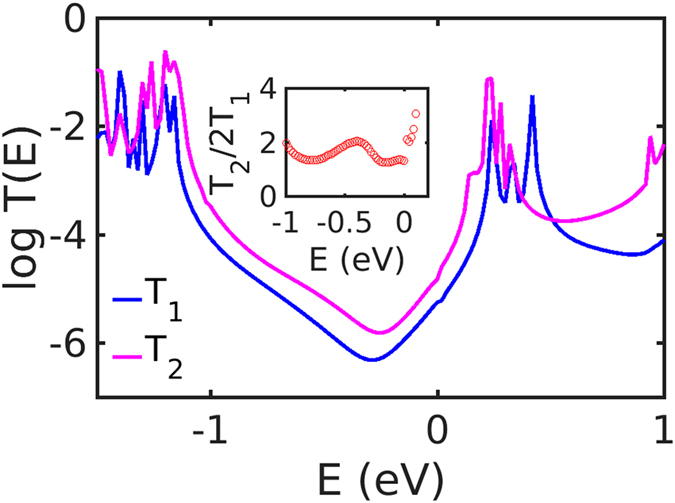
Transmission coefficients of electrons of energy E passing from electrode 1 to electrode 4. The blue and pink curves show the transmission coefficients T 1(E) and T 2(E) of the C60-monomer and -dimer devices, respectively. The inset figure shows the ratio of the two transmission coefficients.
Consequently, the Seebeck coefficient is proportional to the slope of natural logarithm of transmission function at the Fermi level and since these slopes differ, the Seebeck coefficients of the monomer and dimer junctions are different.
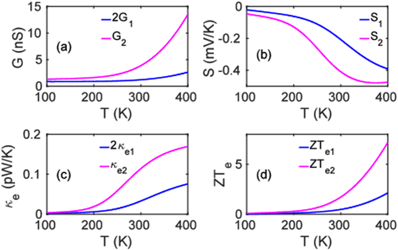
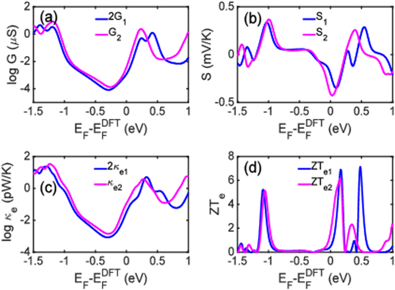
Figure 3 demonstrates that G, S, the electronic contribution to the thermal conductance κ e and the electronic contribution to the thermoelectric figure of merit behave non-classically over a wide range of temperatures. Figure 3(a) shows that the electrical conductance of the dimer system (pink curve) is more than twice the conductance of the monomer (blue curve) over a wide temperature range. Figure 3(b) reveals that the Seebeck coefficient of the dimer junction is higher than that of the monomer junction. Figure 3(d) shows that although the electronic contribution to the thermal conductance (Fig. 3(c)) of the dimer junction is higher than that of the monomer device, the higher electrical conductance and Seebeck coefficient of the dimer junction combine to deliver a higher electronic figure of merit. Since the Fermi energy of the electrodes may be changed by doping or external gating, we analyze in Fig. 4 the quantum behaviour of the thermoelectric properties of the junctions as a function of the Fermi energy at room temperature. Figure 4(a) and (c) demonstrate that both the electrical conductance and the electronic contribution to the thermal conductance of the dimer device are more than twice those of the monomer junction over an energy window around the Fermi energy. Figure 4(b) reveals that the dimer configuration also has a larger absolute value of the Seebeck coefficient than the monomer in the energy range between −0.2 and 0.1 eV and also from 0.3 to 0.5 eV. Figure 4(d) demonstrates that ZT e is also larger in the vicinity of E F.
Figure 3.
Temperature evolution of the thermoelectric coefficients: (a) Electrical conductance G(T); (b) Seebeck coefficients and (c), (d) electronic contribution to thermal conductance and figure of merit . The pink and blue curves correspond to the dimer and twice the monomer devices, respectively.
Figure 4.
(a) Electrical conductance ; (b) Seebeck coefficients and (c), (d) electronic contribution to thermal conductance and figure of merit as a function of the Fermi level at room temperature. The blue and pink curves represent the dimer and twice the monomer devices.
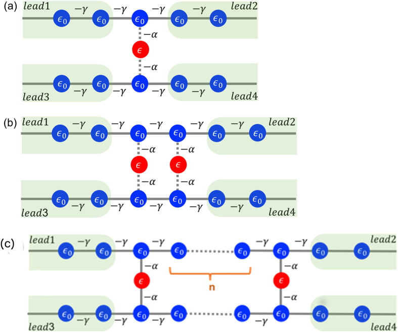
In order to obtain further insight into this quantum interference effect, we have performed calculations of model tight-binding structures that share similar parallel electron pathways to the devices shown in Fig. 1. The schematics of those model structures is shown in Fig. 5. The red balls representing C60 molecules are sandwiched between the blue chains representing the graphene electrodes. There is no direct hopping between the two red sites in the two-site model as in the C60-dimer DFT calculation. Therefore, any departure from Ohm’s law must be due to the indirect coupling between the two sites arising from quantum interference via the electrodes.
Figure 5.
Tight binding models having (a) a One-atom pathway; (b) Two-atom pathways. The chains represent the graphene electrodes, where the blue dots correspond to carbon atoms; the red dots represent the C60 molecules. To fix the energy scale, the hopping integral γ between blue sites is set to unity. The hopping integral α between a red and a blue site is set to 0.2. The hopping integral between red sites in (b) is set to zero. The on-site energy of both blue and red sites ε 0 and ε is set to 0.25. This reflects the relevant energy level landscape found in the DFT calculation and displayed in Fig. 2. (c) A modification of two-site model in (b), where n represents the separation between red sites evaluated by the number of blue sites lying in between.
The transmission coefficients T 2, T 1 and the ratio T 2/(2T 1) of these models are displayed in Fig. 6(a). The pink curve shows that for the two-site model, the transmission resonance at energy E = ε is split in two due to the indirect coupling via the electrodes. The ratio T 2/(2T 1), shown in Fig. 6(b) varies from approximately 0.5 to 2.5 and converges to a constant value around 2, which is twice the expected classical value of unity. Consequently, despite the simplicity of the tight binding model, we find that it captures the mechanism underlying the quantum interference effects uncovered in the DFT-based analysis.
Figure 6.
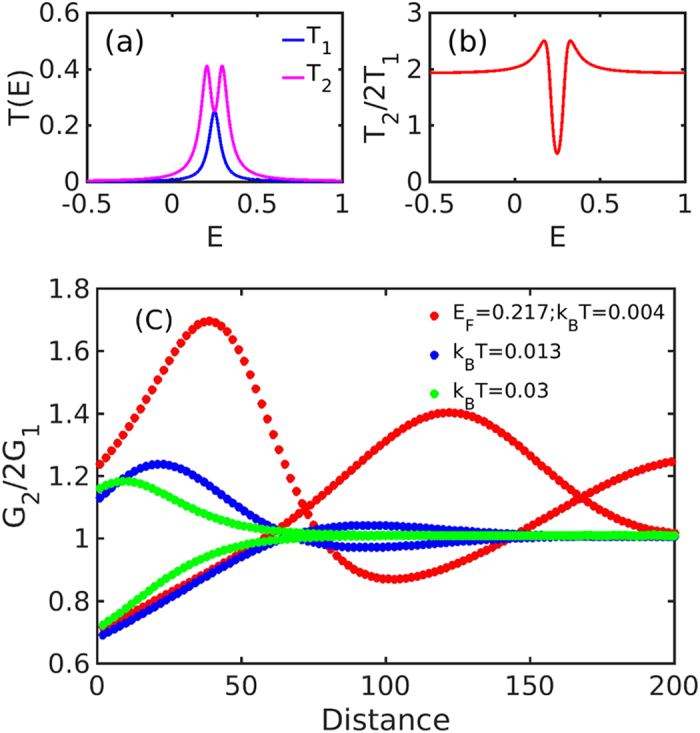
(a) Transmission coefficients as a function of energy E for the one-site and two-site models shown in Fig. 5; The blue line stands for ; (b) Ratio T 2(2T 1). (c) Conductance ratio evaluated at and different temperatures: , 0.013 and 0.03 (red, blue and green lines, respectively); The two curves at each temperature show the conductance ratio for even and odd n.
We now discuss how this quantum interference behaviour depends on the distance between the two sites. To do so, we modify the model shown in Fig. 5(b) and displace the two red sites laterally so that there are n blue sites in between them as shown in Fig. 5(c). Figure 6(b) shows the conductance ratio at three different temperatures (low, intermediate and high). We find that the ratio varies periodically with the distance n, and that it has an envelope that decreases with increasing n. We also find an even-odd quantum interference effect in the conductance ratio as a function of the parity of n. We therefore plot two curves for each temperature, one for even n and another for odd n. The Figure also shows that this low-temperature oscillatory behaviour is damped as the temperature increases. This damping is controlled by the temperature-dependent phase coherence length, and can be understood straightforwardly from the standard expression of the conductance , where G 0 is the conductance quantum unit and the integral L 0 is defined in Eq. (1). The integration window for L n covers an energy range of order that is centered at the Fermi energy. Because the period of the oscillations in T(E) are energy-dependent and the different contributions to the integral dephase, the conductance oscillations die away at values of n beyond a certain dephasing length that is inversely proportional to the temperature, as illustrated in Fig. 6. Interestingly, in the absence of inelestic scattering, the asymptotic ratio does not approach unity for large distances n, even though the oscillations disappear above a certain temperature. This is because the asymptotic ratio depends on the position of the Fermi energy relative to the quantum interference-split resonance shown in Fig. 6(a). The above behaviour is analogous to that of AlGaAs/GaAs quantum rings, where the temperature-dependent phase coherence length, extracted from Aharonov-Bohm magnetoresistance measurements, decreases as the temperature rises above 2.0 K28. The result also agrees well with that obtained by magneto-transport experiments combined with weak localization theory in MgZnO thin film29, where the phase coherence length varies from 38.4 nm to 99.8 nm when temperature declines from 50 K to 1.4 K.
Conclusion
The electrical conductance G 2 of two parallel C60 molecules sandwiched between two graphene monolayers does not follow Ohm’s law, because it is more than twice larger than the conductance G 1 of a single C60 molecule. This non-classical behaviour is due to indirect inter-molecular quantum interference effects mediated by the electrodes. Furthermore, increasing the number of C60 molecules sandwiched in parallel between graphene monolayers from one to two also increases the Seebeck coefficient, which is another non-classical effect. This is significant because it demonstrates that single-molecule thermoelectric properties will not translate into thin-film materials formed from self-assembled monolayers in a classical manner and by exploiting quantum interference, the thermoelectric performance of such SAMs can exceed classical expectations. Further insight into this quantum interference effect is gained by analyzing a tight binding model that features parallel electron transport through two sites. The model predicts that the thermoelectric properties of the dimer will oscillate with the dimer separation n up to a phase coherence length, which decreases with increasing temperature.
Methods
The vertical four-terminal devices shown in Fig. 1(b) and (c) are assigned periodic boundary conditions in the x and y directions. Furthermore, to eliminate edge effects in the z direction, the four regions (labelled leads 1–4) are semi-infinite crystalline leads, which channel electrons to and from reservoirs placed at infinity. In the case of the C60-dimer, the horizontal distance between the nearest atoms of the two C60s is initially set to 6 Å to avoid direct coupling between the buckyballs. We have used the DFT code SIESTA30 to obtain the optimized geometry adopting the local density approximation and the Ceperley-Alder functional for exchange and correlation. We have also chosen a double-z plus polarization (DZP) basis set. After relaxing this structure using about a thousand molecular dynamics steps of 1 fs, this distance is changed by only a fraction of an Å. In this situation, examination of the pseudo-atomic-orbital-based hamiltonian describing the molecules confirms that there is no direct interaction between the two C60 molecules. We have extracted the resulting mean-field Hamiltonian and overlap matrices and used them to compute the electrical and thermoelectric properties of the devices with our transport code GOLLUM31. The transmission coefficient for electrons of energy E travelling from lead i to lead j is calculated through the standard expression32
| 2 |
where G(E) is the device’s retarded Green’s function and is the imaginary part of the self-energy of electrode i. The thermoelectric coefficients including the electrical conductance G, the thermopower S, the electronic contribution to the thermal conductance and to the figure of merit can be written using standard text-book formulae32,33.
| 3 |
| 4 |
| 5 |
| 6 |
in terms of the Lorenz numbers
| 7 |
where is the conductance quantum, h is Planck’s constant, e is the absolute value of electron’s charge, is the mean temperature of electrodes i and j, f is the Fermi-Dirac distribution function and μ is the chemical potential of the device at equilibrium, e.g.: when all leads voltages are set to zero. The specific implementation is explained in detail in the reference article of the GOLLUM code31.
Acknowledgements
H.S. thanks UK EPSRC for a post doctorate position funded by Quantum Effects in Electronic Nanodevices (QuEEN) Program grant. This work was also supported by UK EPSRC (grant nos. EP/M014452/1 and EP/N017188/1), the Spanish Ministerio de Economía y Competitividad (grants FIS2012-34858 and FIS2015-63918-R) and the European Commission FP7 ITN “MOLESCO” (project no. 606728). J.F. wishes to acknowledge discussions with H.S.J. van der Zant and N. Agrait.
Author Contributions
J.F., C.J.L. and H.S. conceived and conducted the project. Q.W. and H.S. carried out the calculations. J.F. performed the Molecular Dynamics calculations. Q.W., H.S., J.F. and C.J.L. wrote the manuscript. All authors took part in the discussions and reviewed the manuscript.
Competing Interests
The authors declare that they have no competing interests.
Footnotes
Publisher's note: Springer Nature remains neutral with regard to jurisdictional claims in published maps and institutional affiliations.
Contributor Information
Hatef Sadeghi, Email: h.sadeghi@lancaster.ac.uk.
Jaime Ferrer, Email: ferrer@uniovi.es.
Colin J. Lambert, Email: c.lambert@lancaster.ac.uk
References
- 1.Heinrich BW, Rastei MV, Choi D-J, Frederiksen T, Limot L. Engineering negative differential conductance with the cu(111) surface state. Phys. Rev. Lett. 2011;107:246801. doi: 10.1103/PhysRevLett.107.246801. [DOI] [PubMed] [Google Scholar]
- 2.García-Suárez VM, Lambert CJ. Non-trivial length dependence of the conductance and negative differential resistance in atomic molecular wires. Nanoechnology. 2008;19:455203. doi: 10.1088/0957-4484/19/45/455203. [DOI] [PubMed] [Google Scholar]
- 3.Chen J, Reed MA, Rawlett AM, Tour JM. Large on-off ratios and negative defferential conductance in a molecular electronic device. Science. 1999;286:1550. doi: 10.1126/science.286.5444.1550. [DOI] [PubMed] [Google Scholar]
- 4.Taylor J, Guo H, Wang J. Physical Review B. 2001;63:121104. doi: 10.1103/PhysRevB.63.121104. [DOI] [Google Scholar]
- 5.Emberly EG, Kirczenow G. The smallest molecular switch. Phys. Rev. Lett. 2003;91:188301. doi: 10.1103/PhysRevLett.91.188301. [DOI] [PubMed] [Google Scholar]
- 6.Baer R, Neuhauser D. Phase coherent electronics: A molecular switch based on quantum interference. Jurnal of the American Chemical Society. 2002;124:4200. doi: 10.1021/ja016605s. [DOI] [PubMed] [Google Scholar]
- 7.Paulsson M, Datta S. Thermoelectric effect in molecular electronics. Phys. Rev. B. 2003;67:241403. doi: 10.1103/PhysRevB.67.241403. [DOI] [Google Scholar]
- 8.Aradhya SV, Venkataraman L. Single-molecule junctions beyond electronic transport. Nature Nanotechnology. 2013;8:399. doi: 10.1038/nnano.2013.91. [DOI] [PubMed] [Google Scholar]
- 9.García-Rincón, L. et al. Molecular design and control of fullerene-based bi-thermoelectric materials. Nature Materials (2015). [DOI] [PubMed]
- 10.Evangeli C, et al. Engineering the thermopower of C60 molecular junctions. Nano letters. 2013;13:2141. doi: 10.1021/nl400579g. [DOI] [PubMed] [Google Scholar]
- 11.Ke S, Yang W, Curtarolo S, Baranger HU. Thermopower of molecular junctions: An ab initio study. Nano letters. 2009;9:1011. doi: 10.1021/nl8031229. [DOI] [PubMed] [Google Scholar]
- 12.Lambert CJ. Basic concepts of quantum interference and electron transport in single-molecule electronics. Chemical Society Reviews. 2015;44:875. doi: 10.1039/C4CS00203B. [DOI] [PubMed] [Google Scholar]
- 13.Klöckner JC, Siebler R, Cuevas JC, Pauly F. Thermal conductance and thermoelectric figure of merit of C60-based single-molecule junctions: electrons, phonons, and photons. Physical Review B. 2017;245404:1–11. [Google Scholar]
- 14.Sadeghi H, Sangtarsh S, Lambert CJ. Enhanced thermoelectric efficiency of porous silicene nanoribbons. Scientific Reports. 2016;5:9514. doi: 10.1038/srep09514. [DOI] [PMC free article] [PubMed] [Google Scholar]
- 15.Karamitaheri H, Pourfath M, Faez R, Kosina H. Geometrical effects on the thermoelectric properties of ballistic graphene antidot lattices. Journal of Applied Physics. 2011;110:054506. doi: 10.1063/1.3629990. [DOI] [Google Scholar]
- 16.Sadeghi H, Sangtarash S, Lambert CJ. Oligoyne molecular junctions for efficient room temperature thermoelectric power generation. Nano letters. 2015;15:7467. doi: 10.1021/acs.nanolett.5b03033. [DOI] [PubMed] [Google Scholar]
- 17.Karamitaheri H, Neophytou N, Pourfath M, Faez R, Kosina H. Engineering enhanced thermoelectric properties in zigzag graphene nanoribbons. Journal of Applied Physics. 2012;111:054501. doi: 10.1063/1.3688034. [DOI] [Google Scholar]
- 18.Garca-Suárez VM, Ferradás R, Ferrer J. Impact of fano and breit-wigner resonances in the thermoelectric properties of nanoscale junctions. Phys. Rev. B. 2013;88:235417. doi: 10.1103/PhysRevB.88.235417. [DOI] [Google Scholar]
- 19.Kim Y, Jeong W, Kim K, Lee W, Reddy P. Electrostatic control of thermoelectricity in molecular junctions. Nature Nanotechnology. 2014;9:881. doi: 10.1038/nnano.2014.209. [DOI] [PubMed] [Google Scholar]
- 20.Reuter MG, Hersam MC, Seideman T, Ratner MA. Signatures of cooperative e ff ects and transport mechanisms in conductance histograms. Nano letters. 2012;12:2243. doi: 10.1021/nl204379j. [DOI] [PubMed] [Google Scholar]
- 21.Sadeghi, H., Sangtarash, S. & Lambert, C. J. Enhancing the thermoelectric figure of merit in engineered graphene nanoribbons. Beilstein J. Nanotechnol.6, 1176 (2015). [DOI] [PMC free article] [PubMed]
- 22.Garca-Suárez VM, Ferradás R, Carrascal D, Ferrer J. Universality in the low-voltage transport response of molecular wires physisorbed onto graphene electrodes. Phys. Rev. B. 2013;87:235425. doi: 10.1103/PhysRevB.87.235425. [DOI] [Google Scholar]
- 23.Sadeghi H, et al. Conductance enlargement in picoscale electroburnt graphene nanojunctions. Proceedings of the National Academy of Sciences of the United States of America. 2015;112:2658–63. doi: 10.1073/pnas.1418632112. [DOI] [PMC free article] [PubMed] [Google Scholar]
- 24.Sadeghi, H., Sangtarash, S. & Lambert, C. J. Robust molecular anchoring to graphene electrodes. Nano Letters acs. nanolett. 7b01001 (2017). [DOI] [PubMed]
- 25.Pai WW, et al. Optimal electron doping of a C60 monolayer on cu(111) via interface reconstruction. Physical Review Letters. 2010;104:036103. doi: 10.1103/PhysRevLett.104.036103. [DOI] [PubMed] [Google Scholar]
- 26.Zheng X, Lu W, Abtew TA, Meunier V, Bernholc J. Negative differential resistance in C60-based electronic devices. ACS Nano. 2010;4:7205. doi: 10.1021/nn101902r. [DOI] [PubMed] [Google Scholar]
- 27.Schull G, Frederiksen T, Brandbyge M, Berndt R. Passing current through touching molecules. Physical Review Letters. 2009;103:11–14. doi: 10.1103/PhysRevLett.103.206803. [DOI] [PubMed] [Google Scholar]
- 28.Aihara K, Yamamoto M, Iwadate K, Mizutani T. Temperature dependence of the phase coherence length of high-mobility algaas/gaas quantum-wire rings. Japanese Journal of Applied Physics. 1991;30:L1627. doi: 10.1143/JJAP.30.L1627. [DOI] [Google Scholar]
- 29.Lv M, et al. Long phase coherence length and anisotropic magnetoresistance in mgzno thin film. Journal of Applied Physics. 2015;117:155304. doi: 10.1063/1.4918541. [DOI] [Google Scholar]
- 30.Soler JM, et al. The siesta method for ab initio order-n materials simulation. J. Phys.: Condens. Matter. 2002;14:2745. [Google Scholar]
- 31.Ferrer J, et al. Gollum: a next-generation simulation tool for electron, thermal and spin transport. New J. Phys. 2014;16:093029. doi: 10.1088/1367-2630/16/9/093029. [DOI] [Google Scholar]
- 32.Datta, S. Electronic transport in mesoscopic systems (Cambridge University Press, 1995).
- 33.Ashcroft, N. W. & Mermin, N. D. Solid State Physics (Brooks/Cole, 1976).


