Abstract
High uniformity Au-catalyzed indium selenide (In2Se3) nanowires are grown with the rapid thermal annealing (RTA) treatment via the vapor-liquid-solid (VLS) mechanism. The diameters of Au-catalyzed In2Se3 nanowires could be controlled with varied thicknesses of Au films, and the uniformity of nanowires is improved via a fast pre-annealing rate, 100 °C/s. Comparing with the slower heating rate, 0.1 °C/s, the average diameters and distributions (standard deviation, SD) of In2Se3 nanowires with and without the RTA process are 97.14 ± 22.95 nm (23.63%) and 119.06 ± 48.75 nm (40.95%), respectively. The in situ annealing TEM is used to study the effect of heating rate on the formation of Au nanoparticles from the as-deposited Au film. The results demonstrate that the average diameters and distributions of Au nanoparticles with and without the RTA process are 19.84 ± 5.96 nm (30.00%) and about 22.06 ± 9.00 nm (40.80%), respectively. It proves that the diameter size, distribution, and uniformity of Au-catalyzed In2Se3 nanowires are reduced and improved via the RTA pre-treated. The systemic study could help to control the size distribution of other nanomaterials through tuning the annealing rate, temperatures of precursor, and growth substrate to control the size distribution of other nanomaterials.
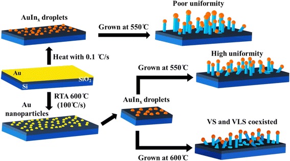
Graphical Abstract.

Rapid thermal annealing (RTA) process proved that it can uniform the size distribution of Au nanoparticles, and then it can be used to grow the high uniformity Au-catalyzed In2Se3 nanowires via the vapor-liquid-solid (VLS) mechanism. Comparing with the general growth condition, the heating rate is slow, 0.1 °C/s, and the growth temperature is a relatively high growth temperature, > 650 °C. RTA pre-treated growth substrate can form smaller and uniform Au nanoparticles to react with the In2Se3 vapor and produce the high uniformity In2Se3 nanowires. The in situ annealing TEM is used to realize the effect of heating rate on Au nanoparticle formation from the as-deposited Au film. The byproduct of self-catalyzed In2Se3 nanoplates can be inhibited by lowering the precursors and growth temperatures.
Keywords: In2Se3, Nanowire, Rapid thermal annealing (RTA), In situ annealing TEM
Background
In the past decade, one-dimensional (1D) nanostructure tubes, wires, rods, and belts have become the focal point of the worldwide research in nanotechnology due to their high performance and surface-to-volume ratios, intrinsically associated with low dimensionality, which may lead to unique applications in the various nanoscale device [1, 2]. In particular, 1D semiconductor nanowires (NWs), exhibiting different properties as compared with their bulk or thin film, have shown great potential applications in data storage, computing, and sensing devices [2–4].
Indium selenide (In2Se3) is a black crystalline and very interesting compound semiconductor of the AIIIBVI group with layered structure, which possessed at least five crystal modifications of α (two-layer hexagonal, 2H), β (three-layer rhombohedral, 3R), γ (defect wurtzite in hexagonal, H), δ, and κ [5, 6]. Due to its polymorphism and the related metal-ion defect structure, In2Se3 has attracted substantial attention as a promising semiconductor material for several different applications such as photovoltaic solar cell [7, 8], optoelectronics [9], and ionic battery [10].
The layered structure of In2Se3 is normally consisting of [Se-In-Se-In-Se] sheets stacked with Se atoms along the c-axis [11–15]. The strong intralayer bonding and weak interlayer Van der Waals interaction lead to highly anisotropic structural, electrical, optical, and mechanical properties [16, 17]. Layer-structure In2Se3 nanowires and nanoribbons have been synthesized by using metal nanoparticles as the catalyst via the vapor-liquid-solid (VLS) process [2, 18–20]. The properties of NWs depend not only on their shape anisotropy but also on their crystallographic anisotropy [21]. The vapor-liquid-solid growth mechanism has been demonstrated to control the diameter and growth direction of nanowires [20–24]. Several research results demonstrated that the catalyst is one of an important part to control the morphology of the nanowires. And the crystallographic orientation of a NW is thermodynamically determined at the liquid-solid (LS) interface within the eutectic liquid droplet of a given size and geometry during the initial nucleation [25, 26]. Also, previous studies have shown that the synthesis of highly uniform semiconductor NWs can be achieved through using the well-defined nanoclusters as catalysts in a VLS growth process [25]. Controlling the growth temperature of the Au-In alloy droplet catalyst can determine the segregation concentrations of In and Se atoms in the Au-In alloy droplet which then affects the diameter of the nanowires. However, Au-catalyzed In2Se3 nanowires are usually grown at relatively high temperature, > 650 °C. According to the Au-In phase diagram, the eutectic temperature is about 530 °C, and the In and/or Se will be precipitated from the Au-In liquid alloy, then reacted with Se to grow the In2Se3 NWs [27]. In this work, rapid thermal annealing (RTA) is used to make the Au film transfer to uniform Au nanoparticles. Furthermore, lower precursor and growth temperature are chosen to reduce the diameter of nanowires and prevent the VS-grown In2Se3 byproducts. Interestingly, the thinner In2Se3 NWs can obtain the diameter by controlling the growth temperature as low as 550 °C. The in situ annealing transmission electron microscopy (TEM) is used to study the effect of heating rate on the Au nanoparticle formation from the as-deposited Au film.
Experimental
The In2Se3 NWs were synthesized in a quartz-tube furnace system with a two-temperature zone. Traditionally, the In2Se3 powder (99.9%, CERAC) was used as a precursor then placed upstream in the middle of the tube at 800 °C (heating rate is 0.01 °C/s). The SiO2/Si(100) substrate is coated with a 2.0 nm thick gold film which was placed downstream. The SiO2/Si(100) coated with a 2.0-nm-thick gold film is annealed by RTA, at 550 °C (heating rate is 100 °C/s), then the substrate is loaded into the growth furnace tube to grow In2Se3 nanowires with a flow rate of argon gas at 25 sccm and pressure of 1 Torr. The temperatures of the In2Se3 precursor powder at the upstream and the Au-coated substrate at the downstream (growth zone) were ramped up to 800 °C (1.2 °C/s) and 550 °C (0.1 °C/s), respectively, and kept for 30 min. The morphologies and microstructure of the In2Se3 NWs were characterized by scanning electron microscope (SEM, JEOL JSM-6500F) and transmission electron microscopy (TEM, FEI Tecnai™ G2 F20 Field Emission Gun) operating at 200 kV. The chemical composition confirmed by energy dispersive X-Ray spectrometer (EDS) is equipped in TEM. The phase of the In2Se3 NWs is confirmed with an X-ray diffractometer (XRD, D8 DISCOVER SSS Multi-Function High Power). In situ annealing TEM was used to study the effect of heating on Au nanoparticle formation. To prepare in situ heating TEM samples, a 2.0 nm Au film is deposited on a square opening of SiO2/Si3N4 thin film. The thicknesses of the SiO2 and Si3N4 film are 30 and 60 nm, respectively. The 2.0 nm Au film is deposited on the SiO2 side, then loaded into TEM to heat with a heating holder (Gatan 652 double tilt heating holder) in the TEM.
Results and Discussion
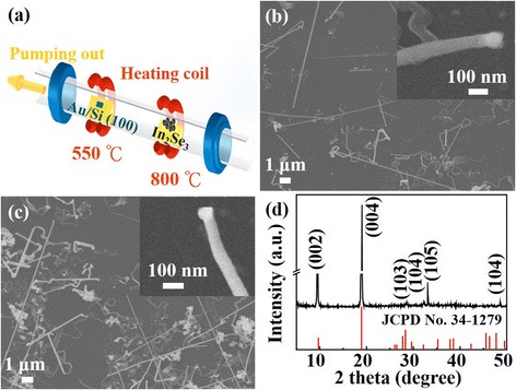
Figure 1a is the schematic illustration of the quartz-tube furnace system that was used to grow the In2Se3 NWs. Typically, the growth window of Au-catalyzed In2Se3 NWs is 650–750 °C and the precursor In2Se3 is heated at 900–950 °C to provide the source of In and Se via a VLS mechanism [19]. However, the Au-In phase diagram shows that the eutectic temperature of Au-In could be as low as 450–550 °C, depending on the composition of the AuInx alloy [28, 29]. It is expected that the diameters of NWs could be controlled by the Au thickness, growth temperature, and the ambient of the furnace. In this work, the temperatures of the growth temperature and In2Se3 precursor powder are set as 550 and 800 °C, respectively. Figure 1b, c are the SEM images of the In2Se3 NWs, grown on the 2.0 nm Au film deposited on a 200-nm SiO2/silicon wafer, with and without rapid thermal annealing (RTA) process, respectively. The bright nanoparticle on the top of the NW can be observed from the inset in Fig. 1b, c, which indicates that the In2Se3 NWs are grown through AuInx nanoparticles via the VLS mechanism. The average diameters of In2Se3 NWs (50 nanowires) with and without the RTA process are 97.14 ± 22.95 nm (23.63%) and 119.06 ± 48.75 nm (40.95%), respectively. The average and distribution of the In2Se3 NW diameters with and without the RTA process are conspicuously different. It clearly exhibits that the RTA process could improve the uniformity and may reduce the diameter of In2Se3 NWs [30–32]. Figure 1d is the XRD result of In2Se3 NWs, and all the peaks can be indexed to the hexagonal crystal structure of α-In2Se3 NWs, in which the lattice constants are a = 4.025 Å and c = 19.235 Å (JCPDS card, no# 34–1279).
Fig. 1.

a Illustration of a two-zone quartz-tube furnace. The In2Se3 powder was used as a precursor and placed upstream in the middle of the tube at 800 °C, and SiO2/Si(100) coated with a 2.0 nm thick Au film was placed downstream and the argon gas as the carrier gas. b and c are the SEM images of In2Se3 nanowires which were grown on the substrate with and without the RTA process, respectively. d A typical XRD spectrum of the Au-catalyzed α-In2Se3 NWs. The lattice constants are a = 4.025 Å and c = 19.235 Å (JCPDS card, No. 34–1279)
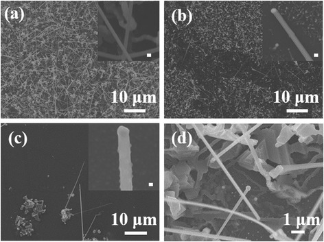
Generally, the Au film-coated substrate is loaded into the furnace, the heating rate usually is 1~2 °C/s, then reacts with the precursor to form a low melting point AuInx alloy, and the In is segregated as the eutectic alloy is supersaturated to react with Se and grow the In2Se3 NW. The slower heating rate results to poor Au nanoparticle uniformity. Not only the thickness and heating rate of Au film on the substrate but the growth temperature is also an important factor to control the morphology of nanowires. Figure 2a–c are the SEM images of the In2Se3 NWs after being RTA-treated then grown at 550, 600, and 650 °C, respectively. The corresponding inset images in Fig. 2a–c showed that the In2Se3 NW diameters were 80–100, 100–200, and 300–500 nm, respectively. The results display that the diameter of In2Se3 NWs could be tuned by controlling the growth temperature. Since the growth temperature was raised, the In solubility in the Au catalyst would be increased; that means the In atoms need more amounts to reach the supersaturated concentration. In the same time, the thicker In2Se3 NWs will be grown through the bigger AuInx droplets. Figure 2d shows the In2Se3 nanowires grown with the precursor temperature at 850 °C (1.3 °C/s). Both of the Au-catalyzed vapor-liquid-solid growth and self-catalyzed vapor-solid (VS) growth In2Se3 nanomaterials, including nanowires, nanoplates, and film, will be obtained simultaneously. The higher precursor temperature will lead to the higher precursor vapor, and the excessive precursor will lead to the In2Se3 product, which tends to self-nucleate and grow. Compared to other studies, the growth temperature, 550 °C, could be much lower than the general reported, 650–750 °C. Furthermore, the precursor temperature could be reduced to 800 °C to prevent self-catalyzed growth. Table 1 lists the comparison of growing In2Se3 nanowire parameters, including growth substrate temperature (heating rate), growth substrate annealing treatment, precursor temperature, and diameter of nanowires. Due to the lower growth temperature, the byproduct is inhibited such that uniform In2Se3 NWs could be obtained at a relatively low temperature. It clearly displays that the In2Se3 NWs could be grown at the lowest growth temperature and precursor temperature in this work. Furthermore, the results of the RTA process showed better diameter uniformity for the In2Se3 NWs than the conventional system, since the diameter of gold particles were confined.
Fig. 2.

SEM images of In2Se3 nanowires which were grown at a 550 °C, b 600 °C, and c 650 °C, respectively; the scale bars of the inset images (a–c) are 100 nm. d In2Se3 nanowires are grown with the precursor and growth temperature at 850 and 600 °C, respectively
Table 1.
Comparison with other works in terms: growth temperature, precursor temperature, and nanowire diameters
| Growth temperature (°C) | Diameter (nm) | RTA | Precursor | Precursor temperature (°C) | Reference |
|---|---|---|---|---|---|
| 650–700 | 40–80 | × | In2Se3 powder | 900–950 | [2] |
| 690 | 80–200 | × | In2Se3 powder | 940 | [5] |
| 690–740 | 150 | × | In2Se3 powder | 920 | [26] |
| 690–740 | 50–200 | × | In2Se3 powder | 920 | [33] |
| 690–740 | 50–200 | × | In2Se3 powder | 930–950 | [34] |
| 550 | 70–150 | ˅ | In2Se3 powder | 800 | in this work |
| 550 | 80–170 | × | In2Se3 powder | 800 | In this work |
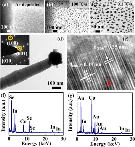
In situ annealing TEM is used to study the effect of heating rate on Au nanoparticle formation and nanowire growth. Figure 3a is the TEM image of the as-deposited 2-nm Au film on the SiO2/Si3N4 window, annealing with 0.1 °C/s and 100 °C/s to 550 °C and holding for 30 min. Figure 3b, c are the results of Au nanoparticle formation with the heating rate at 100 °C/s and 0.1 °C/s, respectively. According to the in situ annealing TEM result, Au nanoparticle average size and distribution are analyzed and listed in Table 2. Briefly, the smaller average size and better uniformity of Au nanoparticles could be achieved through the faster heating rate. Figure 3d is the TEM image of a representative In2Se3 nanowire after being RTA-treated then grown at 550 °C. The result shows that the typical diameter of the nanowire is about 100 nm, and the inset is the corresponding select area electron diffraction (SAED) pattern. Figure 3e shows the high-resolution transmission electron microscopy (HRTEM) image of the corresponding In2Se3 NW that was taken from the [010] zone axis which has lattice spacing of 0.35 and 0.48 nm and can be indexed to the d-spacing of the (100) and (004) planes, which demonstrates that the In2Se3 NW is growing along the [001] direction. The EDS analyses are taken from the top and stem; the results are shown in Fig. 3f, g. The Cu and C signals are contributed from the carbon-coated copper TEM grid. Figure 3f which is taken from the stem is composed of In and Se only, and the atomic ratio of In/Se is approximately 2/3. Figure 3g is the EDS result of the top nanoparticle compositions, including In and Au. The additional Au signal proved that the In2Se3 nanowires are grown via the vapor-liquid-solid (VLS) mechanism. According to the TEM analyses, SEAD, and HRTEM, the VLS-grown nanowires can be identified as α-phase of In2Se3.
Fig. 3.

a 2.0 nm Au film at room temperature. b The gold film by RTA at 550 °C in 100 °C/s. c The gold film was ramped up to the 550 °C in 0.1 °C/s. d TEM image of an as-synthesized individual α-In2Se3 nanowire, with an Au nanoparticle tip. SAED pattern of the α-In2Se3 nanowires (inset). e The corresponding HRTEM image of d shows the growth direction of the nanowire is along the [001]. f and g are the EDS spectra of the selected α-In2Se3 nanowire taken from the body part and the tip part, respectively
Table 2.
The average particle size and standard deviation (SD) of Au nanoparticles annealed with RTA (100 °C/s) and without RTA (0.1 °C/s) through the in situ annealing TEM
| Annealing condition | Average particle size (nm) | SD (nm) | SD (%) |
|---|---|---|---|
| 550_with RTA (100 °C/s) | 19.84 | 5.96 | 30.00 |
| 550_without RTA (0.1 °C/s) | 22.06 | 9.00 | 40.80 |
Conclusions
The lower precursor and growth temperatures 800 and 550 °C, respectively, are provided to grow the Au-catalyzed In2Se3 nanowires by the VLS mechanism. Furthermore, the uniformity of the In2Se3 nanowires could be improved by RTA treatment to reduce the size and distribution of Au nanoparticles. The in situ annealing TEM is used to study the effect of heating rate on Au film transfer to Au nanoparticle. The lower precursor and growth temperatures could reduce the formation of self-catalyzed In2Se3 nanoplates. Lower temperature will lead to lower precursor concentration and low energy, and then the nucleation of self-catalyzed In2Se3 nanoplates could be inhibited the In2Se3 nanoplate byproduct.
Acknowledgements
The research was supported by Ministry of Science and Technology through Grant Nos. MOST 106-2221-E-011-059.
Authors’ Contributions
YHs performed the experiments, analyzed the results, and wrote the manuscript. YHu participated in the sample fabrication and characterizations. CW contributed to the data interpretation, manuscript writing, and supervised the research. All authors read and approved the final version of the manuscript.
Competing Interests
The authors declare that they have no competing interests.
Publisher’s Note
Springer Nature remains neutral with regard to jurisdictional claims in published maps and institutional affiliations.
References
- 1.Zhai T, Ma Y, Li L, Fang X, Liao M, Koide Y, Yao J, Bando Y, Golberg D (2010) Morphology-tunable In2Se3 nanostructures with enhanced electrical and photoelectrical performances via sulfur doping. J Mater Chem 20:6630
- 2.Sun X, Yu B, Ng G, Nguyen TD, Meyyappan M (2006) III-VI compound semiconductor indium selenide (In2Se3) nanowires: Synthesis and characterization. Appl Phys Lett 89:233121
- 3.Law M, Goldberger J, Yang P (2004) Semiconductor nanowires and nanotubes. Rev Mater Res 34:83
- 4.Rao CNR, Deepak FL, Gautam G, Govindaraj A (2003) Inorganic nanowires. Solid State Chem 31:5
- 5.Li Y, Gao J, Li Q, Peng M, Sun X, Li Y, Yuan G, Wen W, Meyyappan M (2011) Thermal phase transformation of In2Se3 nanowires studied by in situ synchrotron radiation X-ray diffraction. J Mater Chem 21:6944
- 6.Jasinski J, Swider W, Washburn J, Liliental-Weber Z, Chaiken A, Nakao K, Gibson GA, Yang CC (2002) Crystal structure of kappa-In2Se3. Appl Phys Lett 81:4356
- 7.Kenawy MA, Mohyi HA, Abo El-Soud AM (1990) A.c. photoconductivity and optical properties of bulk polycrystalline and amorphous InxSe1-x thin films. J Mater Sci Mater Electron 1:115
- 8.Lakshmikumar ST, Rastogi AC (1994) Selenization of Cu and In thin films for the preparation of selenide photo-absorber layers in solar cells using Se vapour source. Sol Energy Mater Sol Cells 32:7
- 9.Ye J, Yoshida T, Nakamura Y, Nittono O (1995) Optical activity in the vacancy ordered III2VI3 compound semiconductor (Ga0.3In0.7)2Se3. Appl Phys Lett 67:3066
- 10.Julien C, Hatzikraniotis E, Chévy A, Kambas K (1985) Electrical behavior of lithium intercalated layered In-Se compounds. Mater Res Bull 20:287
- 11.Julien C, Hatzikraniotis E, Kambas K (1986) Electrical transport properties of impurity‐doped In2Se3. Phys Status Solidi A 97:579
- 12.Zhai T, Fang X, Liao M, Xu X, Li L, Liu B, Koide Y, Ma Y, Yao J, Bando Y, Golberg D (2010) Fabrication of high-quality In2Se3 nanowire arrays toward high-performance visible-light photodetectors. ACS Nano 4:1596 [DOI] [PubMed]
- 13.Zou Y, Chen ZG, Huang Y, Yang L, Drennan J, Zou J (2014) Anisotropic electrical properties from vapor–solid–solid grown Bi2Se3 nanoribbons and nanowires. J Phys Chem C 111:20620
- 14.Lin M, Wu D, Zhou Y, Huang W, Jiang W, Zheng W, Zhao S, Jin C, Guo Y, Peng H, Liu Z (2013) Controlled growth of atomically thin In2Se3 flakes by van der Waals epitaxy. J Am Chem Soc 135:13274 [DOI] [PubMed]
- 15.Suryawansh SR, Bankar PK, More MA, Late D (2015) Vapour–liquid–solid growth of one-dimensional In2Se3 nanostructures and their promising field emission behavior. J RSC Adv 5:65274
- 16.Shen G, Chen D, Chen PC, Zhou C (2009) Vapor solid growth of one-dimensional layer-structured gallium sulfide nanostructures. ACS Nano 3:1115 [DOI] [PubMed]
- 17.Li QL, Liu CH, Nie YT, Chen WH, Gao X, Sun XH, Wang SD (2014) Phototransistor based on single In2Se3 nanosheets. Nano 6:14538 [DOI] [PubMed]
- 18.Yum JH, Walter P, Huber S, Rentsch D, Geiger T, Nüesch F, Angelis FD, Grätzel M, Nazeeruddin MK (2007) Efficient far red sensitization of nanocrystalline TiO2 films by an unsymmetrical squaraine dye. J Am Chem Soc 129:34 [DOI] [PubMed]
- 19.Peng H, Xie C, Schoen DT, Cui Y (2008) Large anisotropy of electrical properties in layer-structured In2Se3 nanowires. Nano Lett 8:1511 [DOI] [PubMed]
- 20.Lai K, Peng H, Kundhikanjana W, Schoen DT, Xie C, Meister S, Cui Y, Kelly MA, Shen ZX (2009) Nanoscale electronic inhomogeneity in In2Se3 nanoribbons revealed by microwave impedance microscopy. Nano Lett 9:1265 [DOI] [PubMed]
- 21.Kuykendall T, Pauzauskie PJ, Zhang Y, Goldberger J, Sirbuly D, Denlinger J, Yang P (2004) Crystallographic alignment of high-density gallium nitride nanowire arrays. Nat Mater 3:524 [DOI] [PubMed]
- 22.Lieber CM (2003) Nanoscale science and technology: building a big future from small things. MRS Bull 28:486
- 23.Yang P (2005) The chemistry and physics of semiconductor nanowires. MRS Bull 30:85
- 24.Wacaser BA, Dick KA, Johansson J, Borgström MT, Deppert K, Samuelson L (2009) Preferential interface nucleation: an expansion of the VLS growth mechanism for nanowires. Adv Mater 20:153
- 25.Wu Y, Cui Y, Huynh L, Barrelet CJ, Bell DC, Lieber CM (2004) Controlled growth and structures of molecular-scale silicon nanowires. Nano Lett 4:433
- 26.Kang D, Rim T, Baek CK, Meyyappan M, Lee JS (2013) Investigation of electromigration in In2Se3 nanowire for phase change memory devices. Appl Phys Lett 103:233504
- 27.Wu Y, Yang P (2001) Direct observation of vapor-liquid-solid nanowire growth. J Am Chem Soc 123:3165
- 28.Dick KA, Deppert K, Mårtensson T, Mandl B, Samuelson L, Seifert W (2005) Failure of the vapor−liquid−solid mechanism in Au-assisted MOVPE growth of InAs nanowires. Nano Lett 5:761 [DOI] [PubMed]
- 29.Bernstein L (1966) Semiconductor joining by the solid‐liquid‐interdiffusion (SLID) process I. J Electrochem Soc 113:1282
- 30.Lin YK, Ting HW, Wang CY, Gwo S, Chou LJ, Tsai CJ, Chen L (2013) Au nanocrystal array/silicon nanoantennas as wavelength-selective photoswitches. J Nano Lett 13:2723 [DOI] [PubMed]
- 31.Ting HW, Lin YK, Wu YJ, Chou LJ, Tsai CJ, Chen LJ (2013) Large area controllable hexagonal close-packed single-crystalline metal nanocrystal arrays with localized surface plasmon resonance response. J Mater Chem C 1:3593
- 32.Wu HW, Chen LJ, Tsai C (2006) Self-assembled epitaxial silicon nanowires grown along easy-glide directions on Si(001). J Micro & Nano Letters 1:25
- 33.Kang D, Rim T, Baek CK, Meyyappan M, Lee JS (2014) Thermally phase-transformed In2Se3 nanowires for highly sensitive photodetectors. Small 10:3795 [DOI] [PubMed]
- 34.Li Q, Li Y, Gao J, Hwang SD, Sun XH (2011) High performance single In2Se3 nanowire photodetector. Appl Phys Lett 99:243105


