Abstract
Gold plasmonic nanostructures with several different adhesion layers have been studied with monochromated electron energy loss spectroscopy in the scanning transmission electron microscope (STEM-EELS) and with surface enhanced Raman spectroscopy (SERS). Compared to samples with no adhesion layer, those with 2nm of Cr or Ti show broadened, lower intensity plasmon peaks as measured with EELS. This broadening is observed in both optically active (“bright”) and inactive (“dark”) plasmon modes. When the former are probed with SERS, the signal enhancement factor is lower for samples with Cr or Ti, another indication of reduced plasmon resonance. This work illustrates the capability of STEM-EELS to provide direct near-field measurement of changes in plasmon excitation probability with nano-scale spatial resolution. Additionally, it demonstrates that applications which require high SERS enhancement, such as biomarker detection and cancer diagnostics, can be improved by avoiding the use of a metallic adhesion layer.
Keywords: Plasmonics, electron energy loss spectroscopy (EELS), Raman spectroscopy, gold nanoparticle, adhesion layers
Graphical abstract
Metal adhesion is a necessary but often ignored aspect of plasmonic device synthesis. Top-down approaches including nanosphere-, photo- and electron beam lithography require a layer between the substrate (typically glass, silicon, or indium tin oxide) and the optically active material (almost always Au or Ag) to avoid delamination. While evaporation of Cr or Ti adhesion layers1–3 is effective, the influence they have on optical device performance is not fully understood. Direct near field observation of plasmon excitation as a function of both energy and position can provide valuable information of both scientific and practical interest.
There have been several optical studies which observe the effects of transition metal adhesion layers by various methods. These include surface enhanced Raman spectroscopy (SERS),4–6 optical scattering spectroscopy7 and fluorescence enhancement spectroscopy8 measurements. All three of these techniques are sensitive to the enhanced local electric field at or around a nanostructure when the incoming photon energy matches a resonant plasmon energy. Greater fields increase the probability of inelastic scattering, elastic scattering, and absorption, thus increasing the signal obtained from each of the above techniques.
In those optical studies, samples generated with Cr or Ti layers beneath the optically active layer are found to generate reduced signal intensities in all three methods as compared to samples with no metal adhesion layer4–8. These studies primarily cite changes in the local real and imaginary dielectric function to explain the effects observed. This in turn affects the way conduction electrons in the material respond to a driving field.5,9 Other proposed mechanisms involve non-radiative dissipation of the plasmon energy, such as Cr or Ti reducing the resonance lifetime due to charge transfer across the metal-metal interface. All of the experimental results from these studies are collected in the optical far-field, and therefore the resolution is diffraction limited. The methods require both excitation and radiative emission in order to collect a signal.
In this work, we aim to compare plasmon excitation of gold nanostructures with no adhesion layer to those with 2nm of Ti or Cr. The limitations of optical techniques – limited resolution, indirect probing of the near field, and inability to excite some plasmon modes – are avoided by the use of electron energy loss spectroscopy in the scanning transmission electron microscope (STEM-EELS). In this technique, an electron probe is focused to the sub-nm scale and rastered over the sample for local mapping of excitation energy and probability.10 This technique has been demonstrated to be capable of measuring dark modes, which only weakly couple to optical excitation, allowing for full characterization of all plasmon resonances present in a structure. 11–14
The same structures are investigated with Raman spectroscopy for comparison. This technique measures inelastic scattering of an excitation laser by a dye molecule. The SERS signal enhancement factor scales with the local electric field enhancement,15 which results from plasmon excitation at the selected laser energy. By choosing relevant laser wavelengths, we gain information complementary to that obtained with EELS regarding the optical response of structures at specific energies.16 Additionally, we show the influence of adhesion layers on the intensity of the SERS signal, which is important for medical applications including biosensing17,18 and cancer detection,19–21 where high signal intensities are critical to ensure sufficient sensitivity.
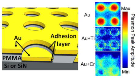
Samples were created for this study by electron beam lithography, followed by evaporation of metallic thin films. For Raman spectroscopy samples, a thin film of polymethyl methacrylate (PMMA) was spin-coated onto a silicon wafer. Regions of the PMMA were exposed to the electron beam and removed with a weak solvent to form the desired pattern. If applicable, an adhesion layer was deposited first, followed by 30nm of Au via electron beam evaporation. A schematic of the final structure, an Au thin film with a square array of round holes (containing Au nanodisks), is shown in Figure 1a. The arrays were then coated with 4-mercaptopyridine Raman dye. SERS testing was performed using 785nm (1.6eV) and 532nm (2.3eV) lasers. A full description of the fabrication can be found in the Methods section at the end of this article.
Figure 1.
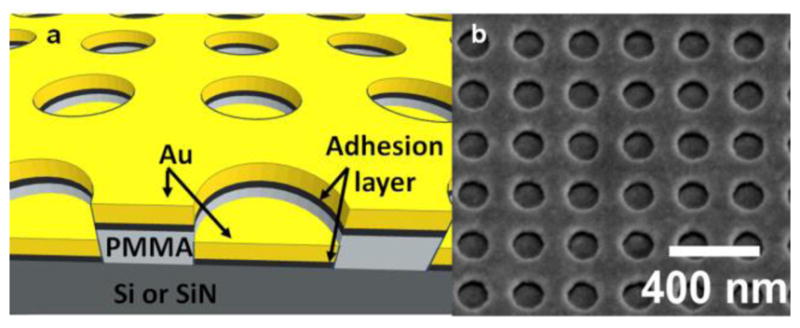
(a) Schematic diagram of the structures investigated. The thicknesses are 30nm for Au, 2nm for the adhesion layer, and ~100nm PMMA. Full details are available in the Methods section. (b) Scanning electron micrograph of the actual structure. The sample is tilted to illustrate better the vertical offset between the gold nanodisks and the surrounding thin film.
In order to create structures thin enough to be electron transparent for STEM-EELS, the procedure described above was modified to use commercially available 35nm thick silicon nitride membranes as a substrate. No dye was applied to these samples to minimize contamination in the electron microscope.
For each sample, monochromated STEM-EELS spectrum images were collected from a region containing four nanodisks near the center of a larger array. Because the data contains a 1D spectrum at each pixel within a 2D image, it can only be fully represented in 3 dimensions. However, selected data is represented in several different ways. Spectra can be plotted from a selected region within the sample. Alternatively, an image – hereafter referred to as an “energy slice” – can be generated by assigning a color based on the number of counts within a particular energy range at each pixel. Both of these methods are used in this work to give a more complete representation of the results. Spectra are background subtracted to compare peak width and position, while raw data is used when comparing relative intensities. Energy slices have been normalized by total counts reaching the detector at each pixel. A full description of the experimental procedures can be found in the Methods section of this paper.
RESULTS AND DISCUSSION
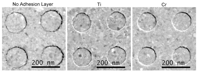
A scanning electron micrograph of one of the arrays is shown in Figure 1b, illustrating the consistency of feature size, shape, and spacing achieved. Three STEM annular dark field images (Figure 2) show the microstructure of arrays with no adhesion layer, Ti, and Cr underlayers respectively from left to right. The speckled contrast is a result of the polycrystalline nature of the evaporated films. No difference in morphology or grain structure between the three samples is observed, suggesting that any changes in plasmon resonance behavior do not result from a physical change in the Au layer.
Figure 2.
Plan view annular dark field scanning transmission electron micrographs of samples with and without an adhesion layer. The speckled contrast is a result of differently oriented grains within the samples. No morphological differences between the three structures are apparent.
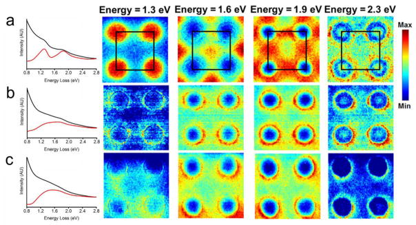
Figure 3 shows EEL spectra before and after background subtraction integrated over a 500nm x 500nm area. The sample with no adhesion layer (top) shows two peaks, while samples with Ti and Cr (middle and bottom respectively) show a single broad peak. The plasmon peak energies observed in all three samples are in agreement with previous EELS studies of gold nanoparticles,12,13 which find resonances in the 1–2.5 eV range.
Figure 3.
Left: Spectra summed over the whole 500 × 500nm region of interest before (black) and after (red) background subtraction of samples with (a) no adhesion layer (b) 2nm Ti and (c) 2nm Cr. Right: Normalized STEM-EELS energy slices generated from the three samples at energies 1.3, 1.6, 1.9 and 2.3 eV. Each slice is generated from a ±0.05eV range of the listed energy and normalized by total detector counts. The four nanodisks shown here are within a larger array, with the array unit cell outlined in black. In order of increasing energy, resonances appear in the sample with no adhesion layer (a) at unit cell corners, face centers, edge centers, and corners again. Samples with Ti (b) and Cr (c) adhesion layers do not show such localized high intensity features.
Energy slices were generated from each spectrum image in 0.1eV intervals. Resonances with four different energies were found in the sample with no adhesion layer, and are shown in Figure 3a. If we define a square unit cell for the array with the center of one nanodisk at each corner, the positions of the resonances can be described. In order of increasing energy, they are: at the array corners at 1.3eV, in the centers at 1.6eV, along edges at 1.9eV and at the corners again, but more localized, at 2.3eV. The 2.3eV resonance has the lowest apparent intensity. Only two of these peaks are apparent in the spatially averaged spectrum, illustrating the need for high resolution methods to fully probe all resonances present in the nanostructure.
When the same energy slices are generated from samples with an adhesion layer, with the same color scale (Figure 3b,c), the results are visibly different. For both samples, and in all four selected energy slices, the localized high intensity features described above are no longer present. Thus we can infer that Cr and Ti reduce the probability of plasmon excitation at the energies selected. In order to address the possibility that peaks had red- or blue-shifted, every energy slice between 1 and 3eV was inspected. However, the periodic high intensity features shown in Figure 3a were not found in either sample with an adhesion layer anywhere within this energy range (Supporting Information, Figure S1).
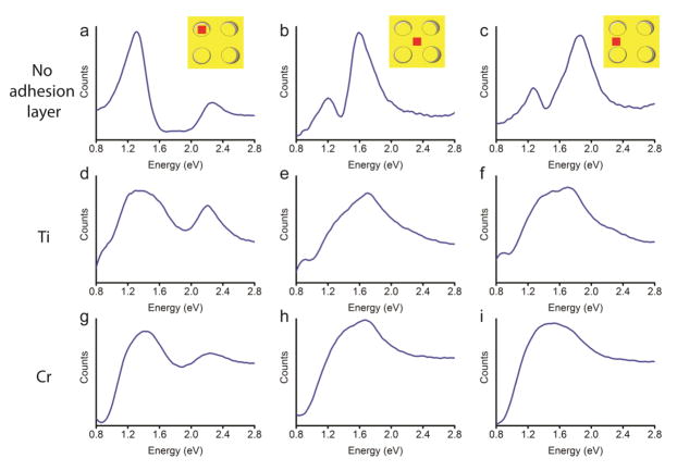
Background subtracted spectra were extracted from each position of interest: the array corners, centers and edges. The spectra give some information which is not visible in the energy slices or the spatially averaged spectra. For example, in the sample without an adhesion layer (Figure 4a–c), there is a peak near 1.3eV at all three positions, but the intensity is much greater at the array corners, where it appears in the energy slice. Additionally, the peaks at 1.6, 1.9 and 2.3eV are easily visible when viewing spectra from each region in the sample separately, unlike in the spatially averaged spectrum in Figure 3a. In the presence of Cr or Ti (Figures 4d–f and g–I respectively), a number of changes occur. The lower energy peak in Figure 4a is broadened in 4d and 4g. The higher energy peak also appears broader, particularly in Figure 4g. The two peaks in Figure 4b are no longer resolved in 4e and 4h. The same is true when comparing Figure 4c with 4f and 4i, with an additional redshift in the peak energy for the latter two. Overall, the peaks are broader and less well defined in the presence of an adhesion layer.
Figure 4.
Background subtracted EEL spectra extracted from different locations (indicated by the inset in each column) for samples with (a–c) no adhesion layer, (d–f) 2nm Ti and (g–i) 2nm Cr. The peaks are broader and less resolved in the presence of an adhesion layer.
Spectra extracted from the array center position without background subtraction are shown in Figure 5, normalized by integrated counts. This data is used to compare relative peak intensities, as small changes in the background fit can result in large changes in calculated counts. In addition to being narrower, the sample with no adhesion shows greater peak intensity. The vertical dashed line marks the energy corresponding to a 785nm laser, which was used to collect SERS data on similar structures fabricated onto a Si wafer. Structures with plasmon energies matching the excitation laser energy are expected to more efficiently collect and emit photons, resulting in an increase in the SERS signal intensity. Therefore, the sample with no adhesion layer, showing the strongest plasmon peak at the marked energy, should demonstrate the greatest enhancement factor. The SERS results, shown in Figure 6, show greater intensity peaks for the sample with no adhesion layer, in agreement with this prediction, as well as previous Raman studies4,5. The relative enhancement factors, as calculated from the peak at 1094cm−1, for the sample with no adhesion layer, Cr, and Ti respectively are 1 (by definition), 0.55, and 0.35.
Figure 5.
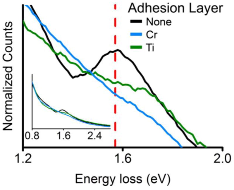
Normalized EEL spectra from array centers without background subtraction. The peak intensity is greater for the sample with no adhesion layer, in addition to being less broad as shown more clearly in Figure 4. The 785nm laser line (vertical dashed line) matches well with the peak energy. The three curves converge at higher and lower energy losses (inset).
Figure 6.
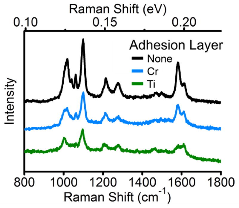
Vertically offset Raman spectra taken from the arrays described in the text using a 1.57eV/785nm laser. The signal intensity is lower for samples with 2nm of Cr or Ti, indicating a lesser local field enhancement.
Although another plasmon peak is present at 2.3eV, Raman spectra collected with a 532nm/2.33eV laser (Figure 7) show no SERS signal from any of the arrays, as explained below.
Figure 7.
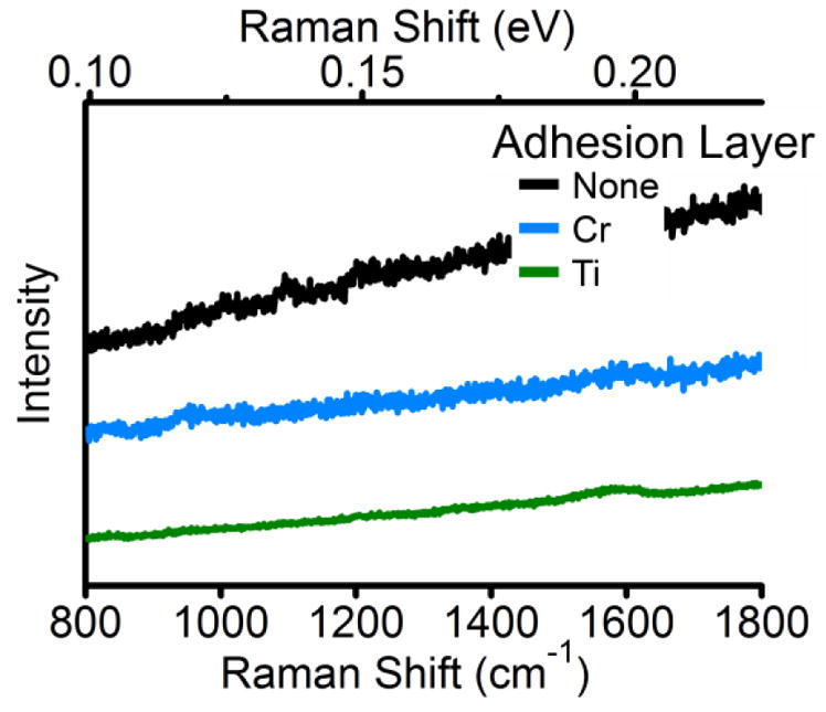
Vertically offset Raman spectra collected using a 2.3eV/532nm laser. No signal is observed for any of the samples, indicating light at this energy does not couple well to the nanostructures, in spite of the 2.3eV peaks observed in EELS.
Resonances which can be excited by an electron beam include both ‘bright’ modes which couple to light and ‘dark’ modes which do not. It has been shown that when an electron beam passes through a sample along a mirror symmetry axis, it can generate a dark resonance with two or more antisymmetric dipole moments which sum to zero12. These types of modes have been demonstrated for several sample and measurement geometries, including passing an electron beam between through the gap between two nearby nanoparticles11,14 or through the center of a round nanodisk22. The latter, referred to as a breathing mode, involves the electron cloud of a metal nanoparticle expanding and contracting radially. The symmetry of the charge distribution results in a vanishing net dipole moment (i.e. the sum of all dipoles over a small volume goes to zero) and therefore they do not efficiently couple to light23. Such modes are found to be excited when the electron probe is placed at the center of a lithographically patterned nanodisk, but not near the edges22. The same excitation pattern is observed in the 2.3eV energy slice in Figure 3a, suggesting the resonance at this energy is a breathing mode.
The idea that the resonance at 2.3eV is a dark mode is further supported by the Raman results. Excitation with a 2.3eV laser does not result in the observation of a SERS signal, in spite of the EELS peak present at that energy, indicating poor coupling of light to the structure. To confirm the mode does not have a dipole moment in the direction normal to the substrate, Raman spectroscopy was also performed with the sample tilted relative to the illumination axis by 10°. Again, no significant signal was found (Figure S2).
In comparison, the excitation at 1.6eV shown in Figure 3a does not have radial symmetry. Therefore, it is not surprising that this resonance is optically active, as indicated by the SERS signal collected using a 1.6eV laser.
The peak width of plasmons measured by EELS has been shown by Bosman et al.24 to be inversely proportional to the quality factor Q of the resonator, and therefore directly proportional to the damping constant of the resonance. Instrumental broadening can be removed in specific scenarios in order to quantify the Q-factor, but requires specific beam conditions. These include collecting spectra several nanometers away from the edge of the metal nanoparticle in an aloof beam setup, such that the electron probe only passes through the silicon nitride support film. This is not possible in the current work due to the sample geometry and our interest in plasmons excited by placing the electron beam directly onto the metal structures. Therefore, we report only a qualitative comparison of the three structures. We find that the same trends of plasmon peak broadening and intensity reduction observed in EELS also appear in Purcell factor simulations of the three structures (Figure S3). Additionally, while the structure geometry is different, the results presented here match the trends predicted by EELS simulations from Nordlander et. al. who compared samples with thicker and thinner Cr adhesion layers.25 They find that a 2.5nm Cr adhesion film results in much lower electron energy loss probability than a sample with only a 1nm film.
Broader plasmon peaks are observed in EELS as a result of both adhesion layers, indicating a decrease in Q-factor, in agreement with previous optical scattering studies9. Additionally, the broadening effect appears more severe in the case of Cr as opposed to Ti. This is attributed to the more dissipative dielectric function of the former.9 The increase in plasmon resonance width suggests that the introduction of an adhesion layer results in shorter lifetimes of plasmonic modes9, which in turn reduces their contribution to far field radiation. As a result, photons which are coupled to these modes have a higher chance of being absorbed by the structure. This explains the diminished SERS intensity observed in Figure 6 and elsewhere.4,5,26 The shape of the features in the Raman spectrum is determined by the dye molecule rather than the plasmonic structure, and therefore no broadening is observed in the SERS data.
Unlike standard optical techniques, the high spatial resolution of STEM-EELS allows resonances excited in different positions within a single nanostructure to be probed separately. While the peaks at 1.6 and 1.9eV overlap in energy and are not both apparent in a spatially averaged spectrum, they are resolved by viewing spectra from different regions less than 100nm apart in the sample.
STEM-EELS also provides the unique ability to measure optically inactive modes. The feature at 2.3eV (Figures 3a,d,g) is one such mode. The same peak broadening effect which was observed in the optically active mode at 1.6eV is apparent here, particularly in the Cr containing sample (Figure 3g). This cannot be confirmed with the SERS data, as no signal is observed for any of the three structures.
CONCLUSIONS
From the results shown above, we conclude that STEM-EELS is sufficiently sensitive to measure changes in plasmon excitation in gold thin films due to the presence of as little as 2nm of a metallic adhesion layer, while providing nanometer scale spatial resolution. Both Cr and Ti cause broadening of the observed plasmon peaks, in agreement with measured SERS signals as well prior optical studies and EELS simulations. Therefore, metallic adhesion layers should be minimized or avoided when generating plasmonic structures which will be excited by light or by electrons, including SERS arrays and structures to be studied by EELS. The link between SERS intensity and plasmon peaks measured with the electron beam continues to be a promising opportunity to develop new structures with greater signal strength, which will improve biosensing and early cancer detection capabilities. Additionally, broadening of an optically inactive peak is observed in EELS, demonstrating the capability of this technique to provide both complementary and new information on plasmon damping in conjunction with optical scattering measurements.
METHODS
Fabrication
Silicon wafers were spin coated with 2% 950,000 molecular weight PMMA in anisole at 2500 rpm, and baked for 5 minutes at 180°C. TEM grids with silicon nitride windows (Ted Pella Inc. 35nm thick 0.5 × 0.5mm) were coated and baked in the same way by adhering the grid to a piece of silicon with polydimethylsiloxane, and affixing the silicon to the spin coater. Prior to lithography, the electron beam tool was run as an SEM to target the small electron transparent windows. Because the electron beam exposes the PMMA resist as it images, it is important not to image the region which will be patterned. To avoid this, the stage positions of two opposite corners of the window are found, and the pattern is exposed at the center, as calculated by the mean position. Electron beam lithography was performed on a JEOL JBX 6300 lithography system using a 100kV 500pA beam. 144nm diameter disks were patterned with a dose of 2000μC/cm2. Arrays of approximately 4×4μm were patterned for STEM-EELS testing, while those for SERS were 30×30μm (e.g. approximately 15,000 disks). These dimensions ensure that both measurements can be performed away from the array edges, where the material response may differ. After lithography, the samples were submerged in a 1:3 methyl isobutyl ketone/isopropanol solution for 30 seconds to dissolve the regions illuminated by the beam. The samples were then rinsed in isopropanol and blown dry with compressed air. Metal depositions were performed in a Kurt J Lesker electron-gun evaporator and film thickness was tracked with a crystal monitor.
Scanning Electron Microscopy
Scanning electron micrographs were collected using an FEI Magellan XHR with a field emission gun source. Secondary electron images were generated using a 5kV beam and collecting signal using an Everhart-Thornley detector.
STEM
STEM-EELS data were collected in an image Cs corrected monochromated FEI Titan 80–300 at 300kV. The monochromator was excited in order to obtain a zero loss peak full width at half maximum ranging from 0.13eV–0.19eV with the probe on the sample. The microscope was operated at spot size 11 with a 38mm camera length, and C2 and C3 apertures of 150 and 50 μm, respectively. Under these conditions the probe size is estimated to be 0.5nm. Spectra were collected with a 2.5nm pixel size and a 0.01eV dispersion using a Gatan Quantum GIF with a 2.5mm entrance aperture. Under these conditions, the convergence and collection angles are 8.4mrad and 18.3mrad respectively. Spectrum collection times were selected to maximize signal without saturating the EELS detector, and ranged from 5–11 ms. Spectrum images sizes were approximately 200×200 pixels.
Surface Enhanced Raman Spectroscopy
Samples for SERS testing were submerged in a 0.1mg/mL aqueous solution of 4-mercaptopyridine. After 4 hours, the samples were removed, rinsed in deionized water, and blown dry with compressed air. Raman spectroscopy was performed on a Horiba LabRam system using a 50x objective to focus the laser to the smallest possible spot, and collected with a 1 second acquisition time. A linear background fit was applied in OriginPro 9.1 to obtain quantitative signal intensities for the peak at 1094cm−1. The resulting values were normalized relative to the sample with no adhesion layer.
Data processing
‘Energy slices’ were generated using a MATLAB script. For each pixel, the number of counts reaching the detector over a 0.1eV energy range was summed, and divided by the total number of counts reaching the detector. This normalizes the fluctuations in the number of counts as a result of thickness variations, Bragg diffraction and other effects. These values are then plotted as a colormap. Spectrum images were imported into MATLAB using a modified version of the algorithm available online at: http://www.mathworks.com/matlabcentral/fileexchange/29351.
Extracted spectra in Fig. 5 were normalized by integrated counts from 0–10eV. Those shown in Figure 4 were background subtracted using power law background subtraction in Gatan DigitalMicrograph software. Curves were smoothed using 5-point adjacent averaging.
Supplementary Material
Acknowledgments
Part of this work was performed at the Stanford Nano Shared Facilities. This research is funded by the Center for Cancer Nanotechnology Excellence for Translational Diagnostics, an NCI-NIH U54 grant (# 1U54CA199075). The authors would like to thank B. Ogut and A. L. Koh for their helpful discussions.
Footnotes
The manuscript was written through contributions of all authors. All authors have given approval to the final version of the manuscript.
Supporting Information Available: S1: Additional EELS energy slices. S2: Raman spectra collected under angled illumination S3: Purcell factor simulations S4: Background subtracted comparison of EELS peak intensities. This material is available free of charge via the Internet at http://pubs.acs.org.
References
- 1.Fromm DP, Sundaramurthy A, Schuck PJ, Kino G, Moerner WE. Gap-Dependent Optical Coupling of Single “ Bowtie ” Nanoantennas Resonant in the Visible. Nano Lett. 2004;4:957–961. [Google Scholar]
- 2.Duan H, Hu H, Kumar K, Shen Z, Yang JKW. Direct and Reliable Patterning of Plasmonic Nanostructures with Sub-10-Nm Gaps. ACS Nano. 2011;5:7593–7600. doi: 10.1021/nn2025868. [DOI] [PubMed] [Google Scholar]
- 3.Mosier-Boss P, Lieberman SH. Comparison of Three Methods to Improve Adherence of Thin Gold Films to Glass Substrates and Their Effect on the SERS Response. Appl Spectrosc. 1999;53:862–873. [Google Scholar]
- 4.Cui B, Clime L, Li K, Veres T. Fabrication of Large Area Nanoprism Arrays and Their Application for Surface Enhanced Raman Spectroscopy. Nanotechnology. 2008;19:145302. doi: 10.1088/0957-4484/19/14/145302. [DOI] [PubMed] [Google Scholar]
- 5.Siegfried T, Ekinci Y, Martin OJF, Sigg H. Engineering Metal Adhesion Layers That Do Not Deteriorate Plasmon Resonances. ACS Nano. 2013;7:2751–2757. doi: 10.1021/nn4002006. [DOI] [PubMed] [Google Scholar]
- 6.Lamy de la Chapelle M, Shen H, Guillot N, Fremaux B, Guelorget B, Toury T. New Gold Nanoparticles Adhesion Process Opening the Way of Improved and Highly Sensitive Plasmonics Technologies. Plasmonics. 2013;8:411–415. [Google Scholar]
- 7.Lahiri B, Dylewicz R, De La Rue RM, Johnson NP. Impact of Titanium Adhesion Layers on the Response of Arrays of Metallic Split-Ring Resonators (SRRs) Opt Express. 2010;18:11202–11208. doi: 10.1364/OE.18.011202. [DOI] [PubMed] [Google Scholar]
- 8.Aouani H, Wenger J, Gérard D, Rigneault H, Devaux E, Ebbesen TW, Mahdavi F, Xu T, Blair S. Crucial Role of the Adhesion Layer on the Plasmonic Fluorescence Enhancement. ACS Nano. 2009;3:2043–2048. doi: 10.1021/nn900460t. [DOI] [PubMed] [Google Scholar]
- 9.Habteyes TG, Dhuey S, Wood E, Gargas D, Cabrini S, Schuck PJ, Alivisatos AP, Leone SR. Plasmon Damping and Molecular Linker as a Nondamping Alternative. ACS Nano. 2012;6:5702–5709. doi: 10.1021/nn301885u. [DOI] [PubMed] [Google Scholar]
- 10.Nelayah J, Kociak M, Stéphan O, García de Abajo FJ, Tencé M, Henrard L, Taverna D, Pastoriza-Santos I, Liz-Marzán LM, Colliex C. Mapping Surface Plasmons on a Single Metallic Nanoparticle. Nat Phys. 2007;3:348–353. [Google Scholar]
- 11.Koh AL, Bao K, Khan I, Smith WE, Kothleitner G, Nordlander P, Maier SA, McComb DW. Electron Energy-Loss Spectroscopy of Surface Plasmons in Single Silver Nanoparticles and Dimers : Influence of Beam Damage and Mapping of Dark Modes. ACS Nano. 2009;3:3015–3022. doi: 10.1021/nn900922z. [DOI] [PubMed] [Google Scholar]
- 12.Chu MW, Myroshnychenko V, Chen CH, Deng JP, Mou CY, García de Abajo FJ. Probing Bright and Dark Surface-Plasmon Modes in Individual and Coupled Noble Metal Nanoparticles Using an Electron Beam. Nano Lett. 2009;9:399–404. doi: 10.1021/nl803270x. [DOI] [PubMed] [Google Scholar]
- 13.Koh AL, Fernández-Domínguez AI, McComb DW, Maier SA, Yang JKW. High-Resolution Mapping of Electron-Beam-Excited Plasmon Modes in Lithographically Defined Gold Nanostructures. Nano Lett. 2011;11:1323–1330. doi: 10.1021/nl104410t. [DOI] [PubMed] [Google Scholar]
- 14.Duan H, Fernández-Domínguez AI, Bosman M, Maier SA, Yang JKW. Nanoplasmonics: Classical down to the Nanometer Scale. Nano Lett. 2012;12:1683–1689. doi: 10.1021/nl3001309. [DOI] [PubMed] [Google Scholar]
- 15.Kneipp K, Wang Y, Kneipp H, Perelman LT, Itzkan I, Dasari RR, Feld MS. Single Molecule Detection Using Surface-Enhanced Raman Scattering (SERS) Phys Rev Lett. 1997;78:1667–1670. [Google Scholar]
- 16.Haynes CL, Van Duyne RP. Plasmon-Sampled Surface-Enhanced Raman Excitation Spectroscopy †. J Phys Chem B. 2003;107:7426–7433. doi: 10.1021/jp050508u. [DOI] [PubMed] [Google Scholar]
- 17.Tripp RA, Dluhy RA, Zhao Y. Novel Nanostructures for SERS Biosensing. Nano Today. 2008;3:31–37. [Google Scholar]
- 18.Sharma B, Frontiera RR, Henry AI, Ringe E, Van Duyne RP. SERS: Materials, Applications, and the Future. Mater Today. 2012;15:16–25. [Google Scholar]
- 19.Zavaleta CL, Smith BR, Walton I, Doering W, Davis G, Shojaei B, Natan MJ, Gambhir SS. Multiplexed Imaging of Surface Enhanced Raman Scattering Nanotags in Living Mice Using Noninvasive Raman Spectroscopy. Proc Natl Acad Sci U S A. 2009;106:13511–13516. doi: 10.1073/pnas.0813327106. [DOI] [PMC free article] [PubMed] [Google Scholar]
- 20.Vendrell M, Maiti KK, Dhaliwal K, Chang YT. Surface-Enhanced Raman Scattering in Cancer Detection and Imaging. Trends Biotechnol. 2013;31:249–257. doi: 10.1016/j.tibtech.2013.01.013. [DOI] [PubMed] [Google Scholar]
- 21.Kircher MF, de la Zerda A, Jokerst JV, Zavaleta CL, Kempen PJ, Mittra E, Pitter K, Huang R, Campos C, Habte F, Sinclair R, Brennan CW, Mellinghoff IK, Holland EC, Gambhir SS. A Brain Tumor Molecular Imaging Strategy Using a New Triple-Modality MRI-Photoacoustic-Raman Nanoparticle. Nat Med. 2012;18:829–834. doi: 10.1038/nm.2721. [DOI] [PMC free article] [PubMed] [Google Scholar]
- 22.Schmidt FP, Ditlbacher H, Hohenester U, Hohenau A, Hofer F, Krenn JR. Dark Plasmonic Breathing Modes in Silver Nanodisks. Nano Lett. 2012;12:5780–5783. doi: 10.1021/nl3030938. [DOI] [PMC free article] [PubMed] [Google Scholar]
- 23.Krug MK, Reisecker M, Hohenau A, Ditlbacher H, Trügler A, Hohenester U, Krenn JR. Probing Plasmonic Breathing Modes Optically. Appl Phys Lett. 2014;105 [Google Scholar]
- 24.Bosman M, Ye E, Tan SF, Nijhuis CA, Yang JKW, Marty R, Mlayah A, Arbouet A, Girard C, Han MY. Surface Plasmon Damping Quantified with an Electron Nanoprobe. Sci Rep. 2013;3:1312. doi: 10.1038/srep01312. [DOI] [PMC free article] [PubMed] [Google Scholar]
- 25.Cao Y, Manjavacas A, Large N, Nordlander P. Electron Energy-Loss Spectroscopy Calculation in Finite-Difference Time-Domain Package. ACS Photonics. 2015;2:369–375. [Google Scholar]
- 26.Okumura Y, Jans H, Dorpe P, Van Li J, Minamiguchi M, Shioi M, Vlaminck L, Lagae L, Kawamura T. Robustness of Surface-Enhanced Raman Scattering Substrate with a Mercaptosilane Adhesive Layer for in Vivo Sensing Applications Robustness of Surface-Enhanced Raman Scattering Substrate with a Mercaptosilane Adhesive Layer for in Vivo Sensing Applications. Jpn J Appl Phys. 2015;54:67002. [Google Scholar]
Associated Data
This section collects any data citations, data availability statements, or supplementary materials included in this article.


