Abstract
The waste from semiconductor manufacturing processes causes serious pollution to the environment. In this work, a non-toxic material was developed under room temperature conditions for the fabrication of green electronics. Flexible organic thin-film transistors (OTFTs) on plastic substrates are increasingly in demand due to their high visible transmission and small size for use as displays and wearable devices. This work investigates and analyzes the structured formation of aqueous solutions of the non-toxic and biodegradable biopolymer, chitosan, blended with high-k-value, non-toxic, and biocompatible Y2O3 nanoparticles. Chitosan thin films blended with Y2O3 nanoparticles were adopted as the gate dielectric thin film in OTFTs, and an improvement in the dielectric properties and pinholes was observed. Meanwhile, the on/off current ratio was increased by 100 times, and a low leakage current was observed. In general, the blended chitosan/Y2O3 thin films used as the gate dielectric of OTFTs are non-toxic, environmentally friendly, and operate at low voltages. These OTFTs can be used on surfaces with different curvature radii because of their flexibility.
Keywords: non-toxic, organic thin-film transistors (OTFTs), chitosan, Y2O3, flexible
1. Introduction
For two decades, the global developments of the electronics industry have focused on flexible electronic devices, such as curved full-color displays [1,2] integrated sensors [3], flexible solar cells, and the amazing achievement of E-paper [4,5]. Using a solution-based process achieves many advantages that are cost-effective and simple to fabricate, and produces mechanically flexible thin-film transistors compared to conventional semiconductor technologies, which depend on vacuum-based thin film fabrication [6,7]. In the past decade, eco-friendly, biocompatible, and green materials have been the subject of many economic and scientific projects [8,9,10], and have caused less damage to the environment. Oxide thin films under low annealing temperatures have been fabricated by using an inexpensive “water-inducement” technique [11] that combines a high-k-value YOX dielectric material with an eco-friendly water-inducement process [12]. Because of their superior performance, organic thin-film transistors (OTFTs) can be used to replace conventional thin-film transistors (TFTs). Chitin is a natural amino polysaccharide and is the largest nitrogenous natural organic compound on the planet after protein and the cellulose polysaccharides found in nature [13]. It has many outstanding characteristics, such as biocompatibility, non-toxicity, biodegradability, antimicrobial activity, and excellent mechanical strength, which make it suitable for use in the biomedical field [14,15]. Chitosan can be transformed into chitin and has the same excellent characteristics, such as biocompatibility, biodegradability, non-toxicity, antimicrobial activity, and an outstanding film-forming ability [16,17,18]. Therefore, in previous studies, chitosan has also been used as dielectric layer in organic transistors [19,20]. Yttrium (III) oxide (Y2O3) is a type of rare earth oxide that is non-toxic, thermodynamically stabile, stabile at high temperature (Tm = 2430 °C), and has a high dielectric constant (ε = 15~18), light transparency, and a linear transmittance in the infrared spectra. Y2O3 is commonly known as a high-k dielectric material that can replace SiO2, because it has a high-k dielectrics value and a phase with cubic symmetry. Its lattice constant, a = 10.6 Å, is two times as large as the lattice constant of Si (a = 5.43 Å). Y2O3 can be deposited by different deposition techniques, including pulsed laser deposition (PLD) [21], sputtering metal-organic chemical vapor deposition (MOCVD) [22], and electron beam evaporation [23].
Therefore, due to its high-k-value, non-toxicity, and biocompatibility, Y2O3 nanoparticles were blended into the chitosan solution in this study to improve their dielectric properties and pinholes. To achieve good electrical performance with the chitosan-based metal-insulator-metal (MIM) structure, various concentrations of Y2O3 nanoparticles were blended into the chitosan to decrease the leakage current and improve the depth of the pinholes. Chitosan thin films have an electric-double-layer effect that gives OTFTs the property of low-voltage operation. Furthermore, the thin films of chitosan blended with Y2O3 nanoparticles were used as the dielectric material in OTFTs, and the performance of these OTFTs was enhanced.
2. Experimental
Yttrium (III) oxide (Y2O3) was provided by Alfa-Aesar (Heysham, UK). Chitosan, poly(3-hexylthiophene) (P3HT) and acetic acid were provided by Sigma-Aldrich (St. Louis, MO, USA). All other reagents and anhydrous solvents were obtained from local suppliers and used without further purification, unless otherwise noted.
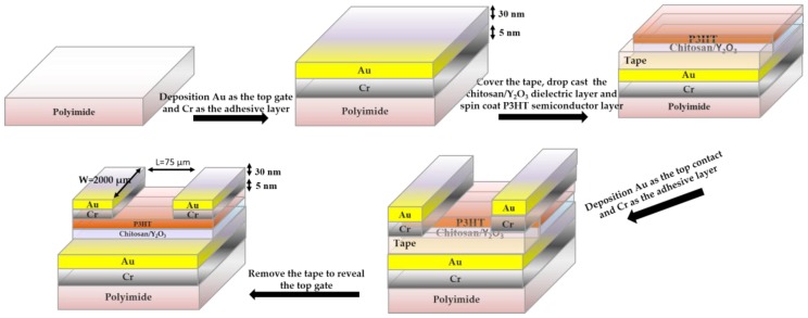
The Y2O3/chitosan thin film as the dielectric gate of the flexible OTFT, and P-type organic semiconductor, poly(3-hexylthiophene) (P3HT), as the semiconductor layer on polyimide substrate were demonstrated in this study. The basic process flow for the fabrication of this flexible device is shown in Figure 1. Moreover, the performance of the flexible OTFT during bending tests with different curvature radii was also observed. In detail, a 5-nm Cr metal layer was deposited as an adhesive layer on the polyimide film by thermal deposition and then a 30-nm Au layer was deposited on the adhesive layer as the bottom gate. The adhesive layer was used to stabilize the Au layer and guarantee that the device would be stable under bending tests. The polyimide substrate was first cleaned before placing it into thermal coater chamber, after which a Cr and Au metal layer was deposited. Before the dielectric layer was deposited, we covered the adhesive tape on the bottom Au electrode, for the bottom gate can only be exposed in the final step.
Figure 1.
The fabrication process of the bottom-gate top-contact flexible organic thin-film transistor.
Chitosan (deacetylated ≥75%) was dissolved in aqueous acetic acid (0.5 wt %) and heated with a hot plate at 50 °C for 24 h, following which its solutions of various concentrations were filtered with a 25-mm syringe filter containing a 0.45-μm polyvinylidene difluoride (PVDF) membrane. The Y2O3 nanoparticles were blended with deionized water at a ratio of 0.5 wt % and the hybrid solution was obtained by mixing chitosan aqueous solution with Y2O3 nanoparticles aqueous solution, with a specific volume ratio CS:Y2O3 (20:1). In other words, the weight percentage of Y2O3 in the blended solutions was 0.023 wt %. The drop casting was used to form the 0.023 wt % Y2O3/chitosan film on the bottom-gate as the dielectric gate, which was then dried in an oven at room temperature for 24 h.
After depositing the dielectric gate, a P3HT channel layer was deposited on the Y2O3/chitosan dielectric film by spin-coating at 1200 rpm for 30 s and then 1500 rpm for 30 s. The polyimide substrate was placed in an oven at 60 °C to remove residual solvent in the P3HT active channel layer. Finally, a 5-nm Cr and a 30-nm Au layer were deposited with a mask to form the source and drain top contacts. Cr metal was used as an adhesive layer between the P3HT channel layer and Au contacts as before. In the meantime, the bottom Au electrode was revealed by carefully removing the tape. Therefore, as the above procedure was finished, the bottom-gate top-contact flexible organic thin-film transistor was successfully designed.
3. Results and Discussion
3.1. Materials and Films Characterization
Chitosan (deacetylated ≥75%) was dissolved in aqueous acetic acid (0.5 wt %) and heated by using a hot plate at 55 °C for 24 h. The impurities in the chitosan solutions of various concentrations were filtered using a 25-mm syringe filter with a 0.45-µm PVDF membrane. The chitosan solution with various concentrations was transferred by spin-coating onto separate single silicon substrates that were already coated with aluminum metal as an electrode by spin-coating. Then, we removed the water in the chitosan thin film by heating on a hot plate at 80 °C for 1 h. Finally, we deposited the aluminum metal as the top electrode on the chitosan, which formed a so-called MIM structure. We found that the lower leakage current was 6.827 × 10⁻¹⁰ A at an applied voltage of 2 V in the MIM based on a 1.0 wt % chitosan thin film, and observed that the 1.0 wt % chitosan film had the lowest leakage current. This result was attributed to the size and the number of the pinholes in the surface of the chitosan, as shown in Figure 2. The thin film with 0.5 wt % chitosan had many small pinholes (10–20 nm), as shown in Figure 2a, and the thin film with 1.5 wt % chitosan had some large pinholes (80–100 nm), as shown in Figure 2c. The thin film with 1.0 wt % chitosan had the optimized hole size (30–50 nm) and number of holes, as shown in Figure 2b; this is why the 1.0 wt % sample had the lowest leakage current.
Figure 2.
(a) 0.5 wt % chitosan shows many small holes (b) 1.0 wt % chitosan shows a few middle-sized holes and (c) 1.5 wt % chitosan shows many large holes.
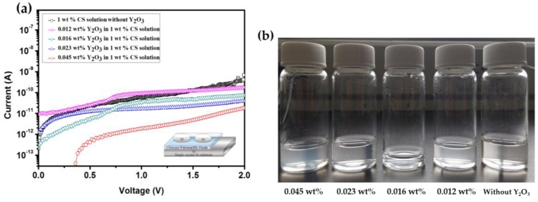
The high-k-value Y2O3 nanoparticles were blended into a 1 wt % chitosan water solution with various weight percentages of Y2O3 (from 0.012 wt % to 0.016 wt %, 0.023 wt % and 0.045 wt %). While the weight percentage increased, the leakage current decreased. The blended 0.045 wt % Y2O3 in 1 wt % chitosan thin film had the lowest leakage current of 1.81 × 10⁻¹¹ A, as shown in Figure 3a. The pure chitosan thin films were almost transparent, the weight percentage of the Y2O3 increased, as shown in Figure 3b. In the meantime, we discovered a decrease in the relative depth (from 1.025 to 0.356 nm) when the concentration of the Y2O3 increased, as shown in Figure 4a–d. However, the relative depth and roughness were increased when the weight percentage of Y2O3 reached 0.045 wt %, as shown in Figure 4e. The purpose of blending the Y2O3 nanoparticles into the chitosan thin film was not to only reduce the leakage current, but also to improve the pinholes at the surface.
Figure 3.
(a) Leakage current of the thin films measured with various concentrations of Y2O3 solutions (without Y2O3, 0.012 wt %, 0.016 wt %, 0.023 wt %, 0.045 wt %) in 1 wt % chitosan solution (b) Pictures showing the various weight percentages of Y2O3 in the mixed solution.
Figure 4.
AFM morphology and profile depth of the pinholes in the surface of the Y2O3/chitosan thin film with various Y2O3 concentrations: (a) Without Y2O3; (b) 0.012 wt %; (c) 0.016 wt %; (d) 0.023 wt %; and (e) 0.045 wt %.
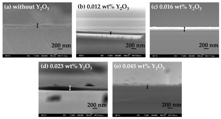
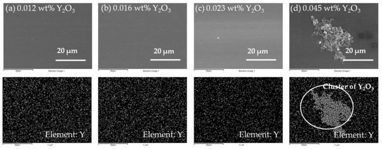
The cross-sectional images of the blended Y2O3/chitosan thin films are shown in Figure 5, and the thicknesses of the blended thin films were approximately 120 nm–200 nm. We also analyzed the distribution of the Y2O3 nanoparticles in the surface of the blended thin films by energy-dispersive X-ray spectroscopy (EDX, JEOL, Freising, Germany). We discovered that the 0.012 wt %, 0.016 wt %, and 0.023 wt % blended thin films showed a uniform dispersion of the Y2O3 nanoparticles, as shown in Figure 6a–c. The Y2O3 nanoparticles attracted each other and clusters formed when the weight percentage of Y2O3 reached 0.045 wt % (Figure 6d). In Figure 4e, we measured the relatively large profile depth of 1.051 nm, and we attributed this phenomenon to the clustering of the Y2O3 nanoparticles. It was observed that the 0.023 wt % thin film had smoothest surface, and its pinholes were much improved.
Figure 5.
Cross-section images of the blended Y2O3/chitosan thin films: (a) Without Y2O3; (b) 0.012 wt %; (c) 0.016 wt %; (d) 0.023 wt %; and (e) 0.045 wt %.
Figure 6.
EDX images showing the distribution of yttrium: (a) 0.012 wt %; (b) 0.016 wt %; (c) 0.023 wt %; and (d) 0.045 wt %.
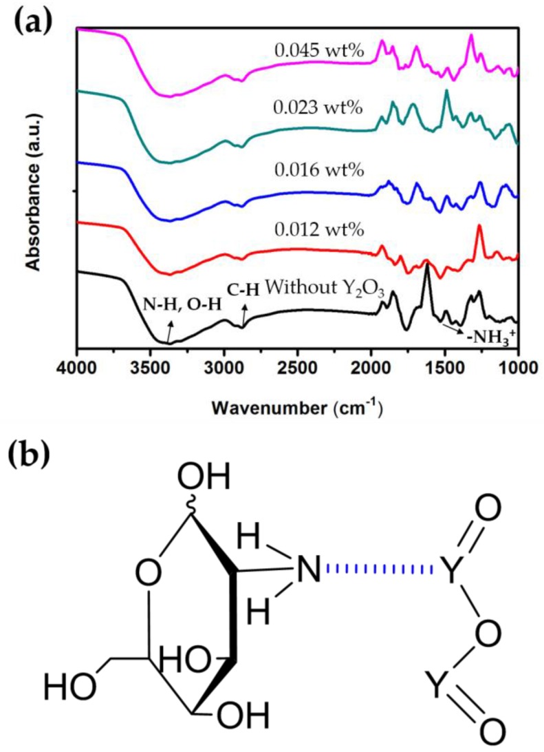
The FTIR spectra analysis (PerkinElmer, Waltham, MA, USA) of the blended Y2O3/chitosan thin films was used to obtain information on the chemical bonding, as shown in Figure 7a. The pure chitosan thin film showed broad absorption peaks at 3000–5000 cm−1 that were attributed to NH2 asymmetric stretching and the hydrogen-bonded OH. The peak at approximately 2879 cm−1 was attributed to the CH3 asymmetric stretching vibrations, and the absorption peak at 1541 cm−1 was attributed to the asymmetric bending modes [24,25,26] of NH3+. Figure 7a also shows the FTIR spectra analysis of all the blended Y2O3/chitosan thin films, which are listed in Table 1. The NH3+ was assigned to the bending frequency at 1541 cm−1 for pure chitosan, which shifted to a higher frequency at 1559 cm−1 and 1580 cm−1 for Y2O3 = 0.012 wt % and 0.016 wt %, respectively, then shifted to a higher frequency at 1598 cm−1 for Y2O3 = 0.023 wt % and shifted to a lower frequency as 1578 cm−1 for Y2O3 = 0.045 wt %. The shifts were due to the H-bonds between the oxygen of yttrium (III) oxide and the amine of chitosan, as shown in Figure 7b. The AFM morphology (Veeco, Plainview, NY, USA) also proved that a dense structure and fewer pinholes were formed by blending Y2O3 nanoparticles into the thin film, as shown in Figure 4.
Figure 7.
(a) FTIR spectra of the blended Y2O3/chitosan thin films; (b) Schematic diagram of hydrogen bonding between the Y2O3 nanoparticles and the amine group of chitosan.
Table 1.
FTIR spectra analysis of the blended Y2O3/chitosan thin film.
| Y2O3 wt % | Wave Number (cm−1) | CH Stretching | NH3+ Bending |
|---|---|---|---|
| O–H and N–H Stretching Broad Absorption Peaks | |||
| n/a | 3368 | 2879 | 1541 |
| 0.012 | 3368 | 2880 | 1559 |
| 0.016 | 3368 | 2880 | 1580 |
| 0.023 | 3367 | 2880 | 1598 |
| 0.045 | 3367 | 2879 | 1578 |
3.2. Electric Characteristics of the Flexible Organic Thin Film Transistor
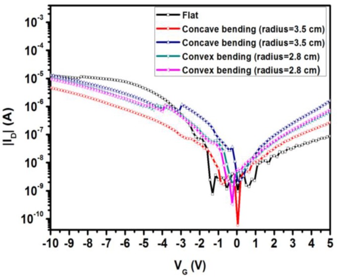
We investigated the electrical properties of the flexible P3HT-based OTFTs with a 0.023 wt % blended Y2O3/chitosan dielectric gate on the polyimide substrate. Figure 8 shows the transfer plots for concave and convex bending of the OTFTs with concave bending radii, R, of 3.5 cm and 2.8 cm and convex bending radii, R, of 3.5 cm and 2.8 cm. In this figure, the electrical characterization of the OTFTs on polyimide substrates without bending is similar to that of the OTFTs on silicon wafers. After concave bending, the Ioff value decreased from 7.421 × 10⁻¹⁰ A to 5.740 × 10⁻¹¹ A due to extrusion, causing a decrease in the size of the pinholes. On the other hand, after convex bending, the Ioff value increased to 1.722 × 10⁻⁹ A. No matter the direction of bending, the Ion value would decrease. In Figure 8, we compared the electrical characterization of the OTFTs with different bending radii (3.5 cm and 2.8 cm), and the comparison chart is listed in Table 2. The output characterization (IDS-VDS) of this device, as shown in Figure S1.
Figure 8.
Comparison of the electrical characterization of the P3HT-based organic thin-film transistors (OTFTs) with a 0.023 wt % blended Y2O3/chitosan dielectric gate for bending tests at different bending radii and without bending.
Table 2.
Electrical characterization of the P3HT-based OTFTs with a 0.023 wt % blended Y2O3/chitosan dielectric gate on the polyimide substrate for bending tests.
| Condition | Vth (V) | Ion (A) | Ioff (A) | Ioff/Ion Ratio | Mobility (cm2/Vs) |
|---|---|---|---|---|---|
| Flat | −2.0 | ||||
| Concave bending 3.50 (cm) | −2.5 | ||||
| Concave bending 2.85 (cm) | −2.7 | ||||
| Flat | −2.1 | ||||
| Convex bending 3.50 (cm) | −3.0 | ||||
| Convex bending 2.85 (cm) | −3.3 | ||||
| Flat | −1.5 |
4. Conclusions
A solution-based processed and low-voltage operating P3HT-based OTFT with a Y2O3/chitosan gate dielectric layer was demonstrated in this study. To improve the electrical performance of the chitosan-based MIM, various concentrations of Y2O3 nanoparticles were blended into the chitosan, which achieved a decreased leakage current and improved the depth of the pinholes. Furthermore, the P3HT-based OTFT with a 0.023 wt % blended Y2O3/chitosan gate dielectric layer was manufactured on polyimide for bending tests. The electrical performance of the flexible device incurred no obvious changes except for a slight increase in the leakage current and off current. The non-toxic and eco-friendly biopolymer chitosan, blended with Y2O3 nanoparticles, was successfully used in flexible OTFTs as the gate dielectric, enabling the OTFT to operate under low voltages, and producing a Ion/Ioff ratio of 105 at a gate voltage of −10 V and a drain voltage of −1 V.
Acknowledgments
The authors would like to thank the Ministry of Science and Technology of Taiwan for supporting this work under Contract MOST 104-2113-M-009-008-MY3 and MOST 105-2622-M-009-004-CC3.
Supplementary Materials
The following are available online at www.mdpi.com/1996-1944/10/9/1026/s1. Figure S1: Output characterization of P3HT-based OTFTs with 0.023 wt % blended Y2O3/chitosan dielectric gate.
Author Contributions
Fu-Hsiang Ko, Ranjohn Singh and Ching-chang Lin designed the experiments. Shao-Ying Hu and Tsung-Tso Tsai carried out the experimental work. Bo-Wei Du wrote the manuscript. All authors contributed to the discussions of this work.
Conflicts of Interest
The authors declare no conflicts of interest.
References
- 1.Forrest S.R. The path to ubiquitous and low-cost organic electronic appliances on plastic. Nature. 2004;428:911–918. doi: 10.1038/nature02498. [DOI] [PubMed] [Google Scholar]
- 2.Li G., Zhu R., Yang Y. Polymer solar cells. Nat. Photonics. 2012;6:153–161. doi: 10.1038/nphoton.2012.11. [DOI] [Google Scholar]
- 3.Vichare N.M., Pecht M.G. Prognostics and health management of electronics. IEEE Trans. Compon. Packag. Technol. 2006;29:222–229. doi: 10.1109/TCAPT.2006.870387. [DOI] [Google Scholar]
- 4.Pagliaro M., Ciriminna R., Palmisano G. Flexible solar cells. ChemSusChem. 2008;1:880–891. doi: 10.1002/cssc.200800127. [DOI] [PubMed] [Google Scholar]
- 5.Jang J. Displays develop a new flexibility. Mater. Today. 2006;9:46–52. doi: 10.1016/S1369-7021(06)71447-X. [DOI] [Google Scholar]
- 6.Fortunato E.M., Barquinha P.M., Pimentel A.C., Goncalves A.M., Marques A.J., Martins R.F., Pereira L.M. Wide-bandgap high-mobility ZnO thin-film transistors produced at room temperature Wide-bandgap high-mobility ZnO thin-film transistors produced at room temperature. Appl. Phys. Lett. 2004;85:2541–2543. doi: 10.1063/1.1790587. [DOI] [Google Scholar]
- 7.Yang Z., Hao J., Yuan S., Lin S., Yau H.M., Dai J., Lau S.P. Field-Effect Transistors Based on Amorphous Black Phosphorus Ultrathin Films by Pulsed Laser Deposition. Adv. Mater. 2015;27:3748–3754. doi: 10.1002/adma.201500990. [DOI] [PubMed] [Google Scholar]
- 8.Arthur T., Harjani J.R., Phan L., Jessop P.G., Hodson P.V. Effects-driven chemical design: The acute toxicity of CO2-triggered switchable surfactants to rainbow trout can be predicted from octanol-water partition coefficients. Green Chem. 2012;14:357–362. doi: 10.1039/C1GC15620A. [DOI] [Google Scholar]
- 9.Hwang S.W., Park G., Edwards C., Corbin E.A., Kang S.K., Cheng H., Lee J.E. Dissolution chemistry and biocompatibility of single-crystalline silicon nanomembranes and associated materials for transient electronics. ACS Nano. 2014;8:5843–5851. doi: 10.1021/nn500847g. [DOI] [PubMed] [Google Scholar]
- 10.Agharkar M., Kochrekar S., Hidouri S., Azeez M.A. Trends in green reduction of graphene oxides, issues and challenges: A review. Mater. Res. Bull. 2014;59:323–328. doi: 10.1016/j.materresbull.2014.07.051. [DOI] [Google Scholar]
- 11.Liu G., Liu A., Zhu H., Shin B., Fortunato E., Martins R., Shan F. Low-Temperature, Nontoxic Water-Induced Metal-Oxide Thin Films and Their Application in Thin-Film Transistors. Adv. Funct. Mater. 2015;25:2564–2572. doi: 10.1002/adfm.201500056. [DOI] [Google Scholar]
- 12.Cao X., Shen F., Zhang M., Bie J., Liu X., Luo Y., Sun C. Facile synthesis of chitosan-capped ZnS quantum dots as an eco-friendly fluorescence sensor for rapid determination of bisphenol A in water and plastic samples. RSC Adv. 2014;4:16597–16606. doi: 10.1039/C3RA47868H. [DOI] [Google Scholar]
- 13.Pillai C.K.S., Paul W., Sharma C.P. Chitin and chitosan polymers: Chemistry, solubility and fiber formation. Prog. Polym. Sci. 2009;34:641–678. doi: 10.1016/j.progpolymsci.2009.04.001. [DOI] [Google Scholar]
- 14.Chung Y.C., Tsai C.F., Li C.F. Preparation and characterization of water-soluble chitosan produced by Maillard reaction. Fish. Sci. 2006;72:1096–1103. doi: 10.1111/j.1444-2906.2006.01261.x. [DOI] [Google Scholar]
- 15.Rinaudo M. Chitin and chitosan: Properties and applications. Prog. Polym. Sci. 2006;31:603–632. doi: 10.1016/j.progpolymsci.2006.06.001. [DOI] [Google Scholar]
- 16.Couto D.S., Hong Z., Mano J.F. Development of bioactive and biodegradable chitosan-based injectable systems containing bioactive glass nanoparticles. Acta Biomater. 2009;5:115–123. doi: 10.1016/j.actbio.2008.08.006. [DOI] [PubMed] [Google Scholar]
- 17.Jayakumar R., Menon D., Manzoor K., Nair S.V., Tamura H. Biomedical applications of chitin and chitosan based nanomaterials-A short review. Carbohydr. Polym. 2010;82:227–232. doi: 10.1016/j.carbpol.2010.04.074. [DOI] [Google Scholar]
- 18.Wan Y., Wu H., Cao X., Dalai S. Compressive mechanical properties and biodegradability of porous poly (caprolactone)/chitosan scaffolds. Polym. Degrad. Stab. 2008;93:1736–1741. doi: 10.1016/j.polymdegradstab.2008.08.001. [DOI] [Google Scholar]
- 19.Morgado J., Pereira A.T., Bragança A.M., Ferreira Q., Fernandes S.C.M., Freire C.S.R., Alcácer L. Self-standing chitosan films as dielectrics in organic thin-film transistors. Express Polym. Lett. 2013;7:960–965. doi: 10.3144/expresspolymlett.2013.94. [DOI] [Google Scholar]
- 20.Liu Y.H., Zhu L.Q., Feng P., Shi Y., Wan Q. Freestanding Artificial Synapses Based on Laterally Proton-Coupled Transistors on Chitosan Membranes. Adv. Mater. 2015;27:5599–5604. doi: 10.1002/adma.201502719. [DOI] [PubMed] [Google Scholar]
- 21.Yi S.S., Bae J.S., Moon B.K., Jeong J.H., Park J.C., Kim I.W. Enhanced luminescence of pulsed-laser-deposited Y2O3: Eu3+ thin-film phosphors by Li doping. Appl. Phys. Lett. 2002;81:3344–3346. doi: 10.1063/1.1517404. [DOI] [Google Scholar]
- 22.Durand C., Dubourdieu C., Vallée C., Loup V., Bonvalot M., Joubert O., Renault O. Microstructure and electrical characterizations of yttrium oxide and yttrium silicate thin films deposited by pulsed liquid-injection plasma-enhanced metal-organic chemical vapor deposition. J. Appl. Phys. 2004;96:1719–1729. doi: 10.1063/1.1766412. [DOI] [Google Scholar]
- 23.Atanassov G., Thielsch R., Popov D. Optical properties of TiO2, Y2O3 and CeO2 thin films deposited by electron beam evaporation. Thin Solid Films. 1993;223:288–292. doi: 10.1016/0040-6090(93)90534-V. [DOI] [Google Scholar]
- 24.Ko Y.G., Lee H.J., Shin S.S., Choi U.S. Dipolar-molecule complexed chitosan carboxylate, phosphate, and sulphate dispersed electrorheological suspensions. Soft Matter. 2012;8:6273–6279. doi: 10.1039/c2sm25250c. [DOI] [Google Scholar]
- 25.Li Z., Zhuang X.P., Liu X.F., Guan Y.L., Yao K.D. Study on antibacterial O-carboxymethylated chitosan/cellulose blend film from LiCl/N, N-dimethylacetamide solution. Polymer. 2002;43:1541–1547. doi: 10.1016/S0032-3861(01)00699-1. [DOI] [Google Scholar]
- 26.Liu X.F., Guan Y.L., Yang D.Z., Li Z., Yao K.D. Antibacterial action of chitosan and carboxymethylated chitosan. J. Appl. Polym. Sci. 2001;79:1324–1335. [Google Scholar]
Associated Data
This section collects any data citations, data availability statements, or supplementary materials included in this article.


