Abstract
We report on a label-free immunosensor based on graphene field effect transistors (G-FETs) for the ultrasensitive detection of Human Chorionic Gonadotrophin (hCG), as an indicator of pregnancy and related disorders, such as actopic pregnancy, choriocarcinoma and orchic teratoma. Pyrene based bioactive ester was non-covalently anchored onto the graphene channel in order to retain the sp2 lattice. The G-FET transfer characteristics showed repeatable and reliable responses in all surface modifying steps using a direct current (DC) readout system. The hCG concentration gradient showed a detection limit of ~1 pg·mL−1. The proposed method facilitates the cost-effective and viable production of graphene point-of-care devices for clinical diagnosis.
Keywords: graphene, field effect transistor, immunosensor, human chorionic gonadotrophin
1. Introduction
Human Chorionic Gonadotrophin (hCG) is a glycosylated protein (37.5 kDa) secreted by placenta during pregnancy or gestational trophoblastic diseases [1,2]. The function of hCG is to stimulate steroid hormone and progesterone production in the corpus luteum to support placental growth [3]. Hence, increased levels of hCG in the serum and urine are key indicators of trophoblastic tumors and other pregnancy related diseases [4,5,6]. As a result, it is significantly important to develop a highly selective and sensitive sensor to detect hCG for early diagnosis. At present, the detection methods for hCG mainly include various immunoassay based on electrochemical, electrochemiluminescence, fluorescence, enzyme, chemiluminescence resonance energy transfer, chemiluminescence and radiation [7]. Though these systems are sensitive and selective, but they tend to be expensive, time-consuming, labor intensive, bulky and require additional electrical system to translate into electrical signals. Hence, there is a need in manufacturing reliable and scalable electrical method to meet the demand for point of care testing (POCT) devices.
Since the first report by Bergveld et al. on FET based immunosensor (immunoFET), numerous studies have been conducted on immunoFET based on silicon nanowires (SiNW), SiO2 nanobelt, ZnO nanofilm, Au nanoparticles, molybdenum disulphide (MoS2), cerium oxide (CeOx) and single-walled carbon nanotubes (SWCNT) to name a few [8,9]. Recently, graphene attracted much interest by various research groups to focus on the possibility of graphene based FET (gFET) due to its unique characteristics regarding high surface to volume ratio, biocompatibility consisting of extreme sensitivity to the environment and ambipolar behavior [10,11,12,13]. Half a dozen of reports has appeared in last few years on back-gated graphene field effect transistor (BG-gFET) immunosensors, indicating that there is a growing interest from both academic and industrial researchers to meet all the challenges for cost-effective, easy to fabricate, scalable, reliable, ultrasensitive and rapid on-site detection devices [14,15,16,17,18,19]. Note that a non-covalent functionalization is of graphene is of much importance as covalent functionalization augments carrier scattering instigated by the conversion of planar sp2 to tetrahedral sp3 carbons leading to charge impurities and vacancy defects. To the best of our knowledge, there is only one report on BG-gFET based immunoassay for hCG detection, using multilayer epitaxial graphene grown on silicon carbide and a covalent functionalization method was used to anchor the necessary biomolecules. Other BG-gFET based immunoassays adopted intermediary modification of graphene either by hexamethyldisilazane (HMDS) or reduced to graphene oxide targeting rotavirus, DNA or cancer biomarkers [15,16,17].
In the present study, we demonstrate a scalable CVD grown monolayer graphene based FET immunosensor on a SiO2/Si substrate. A non-covalent bond between monolayer graphene and antibody was facilitated by applying a linker molecule known as 1-pyrenebutyric acid–N-hydroxysuccinimide ester (Pyr-NHS) via π-π bonding. The performance of the device was assessed under ambient conditions for over 10 devices to establish higher stability and repeatability. Changes in resistance difference between consecutive surface modifications displayed a distinctive pattern not commonly seen in relation to the usual increase in resistance owing to biomolecular absorption. The sensor exhibited an ultralow label-free detection limit of 1 pg·mL−1 with high sensitivity (0.30 Ω·ng−1·mL−1) and reproducibility (>87% yield). An in-depth analysis on carrier transfer for each surface modification was carried out for the first time for non-covalently functionalized BG-gFET illustrating the importance of net charge, amino acid content and the isoelectric point of biomolecules. These key factors are vital for bioelectronic sensing mechanism and device performance. The rapid, sensitive, selective, stable, repeatable and reliable detection suggests promising applications of bgFET structure for multiple marker detection on a point-of-care device.
2. Materials and Methods
2.1. Materials
Monolayer CVD graphene on Cu foil was purchased from Graphene Supermarket (Calverton, NY, USA). Photoresist 1805 G2, lift-off resist 3B (LoR) and their corresponding developer and remover were purchased from A-Gas Electronic Materials (Warwickshire, UK). All the other chemicals, such as Pyr-NHS, iron nitride, nitric acid, PBS, Poly (methyl methacrylate) (PMMA), Ethanolamine etc. at biochemical grade were purchased from Sigma Aldrich (Dorset, UK). Bovine serum albumin (BSA) at biochemical grade was purchased from Sigma Aldrich (Dorset, UK). 100 µg·hCG (ab126652) lyophilized powder and 1 mL of 0.02 mg·mL−1 complementary anti-hCG (ab8466) in PBS buffer were purchased from Abcam (Cambridge, UK) and the prepared aliquots were stored at −20 °C.
2.2. Characterization of BG-gFET
Raman spectra was collected in an XploRA Raman system (Horiba, Middlesex, UK) running a LabSpec 6.4.2.5 and equipped with a 532 nm HeNe laser delivering 20 mW of laser power at the sample. An Olympus BX41 microscope (Olympus Corp., Tokyo, Japan) with a 100 µm slit width, a 300 µm confocal hole, 1200 T grating and 1000× magnification was used. An MPlan N 100× microscope objective (N.A.: 0.90, W.D.: 0.21, F.N.: 22) focused the laser on the sample into a spot of ~7.45 µm diameter. A thermoelectrically cooled charge coupled device (CCD) camera was used for detection. Single spectra were collected for bare, coated and non-coated dentine by graphene from 1100 cm−1 to 3000 cm−1 range with five accumulations each lasting 15 s.
X-ray photoelectron spectroscopy (XPS) was performed with Kratos AXISULTRA with a mono-chromated Al kα X-ray source (1486.6 eV) using an emission current of 10 mA and an anode potential of 12 kV (120 W). The ULTRA was used in fixed analyzer transmission (FAT) mode, with pass energy of 80 eV for wide scans and pass energy 20 eV for high resolution scans. Cyclic Voltammetry (CV) measurements were carried out in 10 mM ferricyanide aqueous solution (1 M KCl solution) at room temperature with a scan potential range from 0.8 V to −0.4 V and a scan rate of 100 mV·s−1.
2.3. Sensor Test and Data Analysis
A Keysight B1500A semiconductor device parameter analyzer with an MPS150 probe station (Cascade Microtech GmbH, Thiendorf, Germany) was employed to investigate the electrical characteristics and sensing performance of the FET device at room temperature. The transistor measurement on the sensor was carried out by measuring the drain current (Ids) as a function of the gate voltage (Vg) (−100 V to +100 V) with a fixed drain-source voltage (Vds = 100 mV). The sensing signal of the device was recorded by monitoring the Ids as a function of drain-source voltage (Vd) (−1 V to +1 V) with a fixed gate voltage (Vds = 0 V). The data were analysed using SigmaPlot 13 software (Systat Software Inc, London, UK).
2.4. Wet Transfer of Graphene
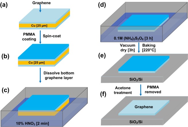
The monolayer graphene was obtained from Graphene Supermarket (Calverton, NY, USA), and it was synthesized on both sides of 25 µm thick copper foil through chemical vapour deposition (CVD) method [20]. The wet transfer process as shown in Figure 1 was used to transfer monolayer graphene onto SiO2/Si substrates as follows. Firstly, PMMA was dissolved in the chlorobenzene with a 10 mg·mL−1 concentration and spin-coated on the one side of the graphene film at a spin speed of 4000 rpm for 30 s followed by baking at 180 °C for 1 min. To etch the Cu substrate, 10% HNO3 was used for 2 min followed by etching in 0.1 M ammonium persulfate for approximately 3 h with the endpoint determined when Cu was no longer visible. The resulted PMMA/graphene membrane was transferred to a rinse bath of deionized (DI)water for 10 min. Subsequently, monolayer graphene was directly transferred onto SiO2/Si substrates. Finally, PMMA layer was removed by acetone treatment at 50 °C for five minutes following by cleaning with Isopropyl alcohol (IPA) and DI water. Graphene on SiO2/Si substrates obtained as such was dried in vacuum before characterization and measurements.
Figure 1.
Schematic illustration of graphene wet transfer on SiO2/Si. The process begins with a graphene monolayer on Cu foil (a); After depositing a support layer composed of PMMA (b); the bottom graphene layer and Cu layer are etched by floating the sample on a HNO3 and (NH4)2S2O8 respectively (c,d); After transferring the resulting graphene-PMMA bilayer on a SiO2/Si substrate, PMMA removal by acetone (e,f) completes the transfer process.
2.5. Materials Fabrication of hCG Biosensor
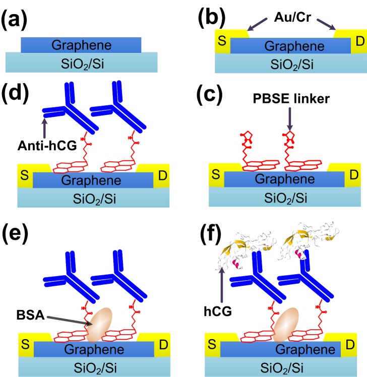
A schematic illustration of the fabrication of hCG biosensor is shown in Figure 2. A flexible monolayer-layer graphene film on SiO2/Si substrate was obtained by wet-transfer method as mentioned above [21,22]. In order to fabricate source-drain and voltage electrodes, two consecutive photolithography was conducted. The lithography process begins with spin-coating LoR and positive photoresist (pPR) at 3000 rpm for 30 s. LoR was pre-baked at 175 °C for 15 min followed by soft-baking of spin-coated pPR at 100 °C for 1 min. For shaping graphene channel, samples were hard-baked at 180 °C for about an hour under deep UV (DUV) to reduce the pPR effect on graphene channel as much as possible [19]. We used a modified Argon plasma method to sputter the graphene on SiO2/Si at 50 W and 6 × 10⁻⁷ Torr for 2 min [23]. We deposited 5 nm Cr puddles for contact by thermal evaporator followed by 30 nm of Au layer by sputtering at 2 × 10⁻⁷ Torr and 4 mTorr base and Ar pressure [24]. The thickness of SiO2 is 300 nm and the width and length of each FET unit is 90 µm and 80 µm respectively.
Figure 2.
Schematic illustration of hCG biosensor fabrication. (a) monolayer graphene on SiO2/Si substrate; (b) Fabrication of BG-gFET; (c) anchoring of non-covalent linkers by π-π bond; (d) immobilization of antibodies; (e) blocking by BSA; (f) binding of hCG antigen.
Pyr-NHS was used as the linker between graphene channel and anti-hCG via π-π interaction. Consisting of hydrophobic pyrenyl moiety base and a bio-active ester head, Pyr-NHS does not require any pre-treatment of antigen with EDAC/NHS chemistry is required [14]. 2 mM Pyr-NHS solution was prepared by adding 0.0385 g Pyr-NHS powder into 5 mL methanol with modest shaking for 5 h. The linker solution was drop-casted on BG-gFETs and sealed in a moist environment for 2 h at room temperature, followed by methanol rinsing to avoid passivation layer formation. The functionalized graphene channels were covered by 10 µg·mL−1 anti-hCG solution and incubated at 4 °C for 4 h. The surface of graphene channel was rinsed with PBS buffer and immersed in BSA solution with a concentration of 0.5 mg·mL−1 to block the free amino groups to prevent the non-specific binding of hCG. Finally, hCG solution with concentrations ranging from 1 pg·mL−1 to 100 ng·mL−1 were prepared by diluting 1 µg·mL−1 stock solution with PBS buffer and then incubated on graphene channel at 4 °C for 4 h to ensure the strong antibody/antigen binding. Finally, the samples were treated with 100 mM ethnolamine for 30 min and washed with DIW for 5 min to remove non-specific passivation followed by vacuum dry at 30 Torr for an hour before characterization [25].
3. Results and Discussion
3.1. Assessment of Surface Morphology
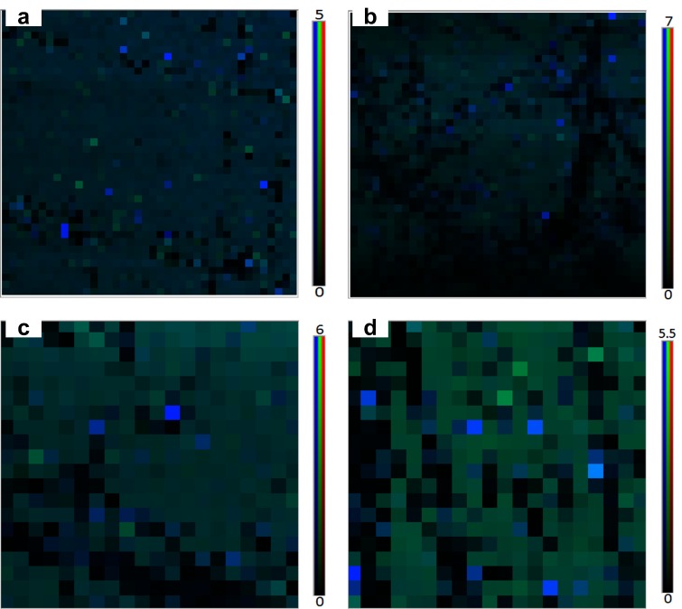
The morphology of the samples and surface modification was characterized by Raman spectroscopy, XPS and cyclic voltammetry. Figure 3 shows raman maps of 2D/G for graphene/SiO2 before and after adding linker and others. The intensity ratios of 2D-band to G-band are higher than 5. These data confirm that the transferred graphene before and after treating with linker and others is high-quality and continuous. For effective removal of photoresist during fabrication, deep UV (DUV) technique was used within the fabrication process to reduce photoresist contamination. The details of our work to obtain clean, uniform, and continuous graphene, with a typical low sheet resistance along with XPS and Cyclic voltammetry analysis have been elaborated in our recent works in detail [19,23]. The results demonstrated effective reduction of sheet resistance and contact resistance on the graphene surface by about 60% and 80%, respectively. Electrical current transport characteristics also demonstrated minimizing this residue on the graphene surface giving less hysteresis of electronic transport in BG-gFETs.
Figure 3.
Raman maps of 2D/G for (a) bare graphene/SiO2; (b) linker + graphene/SiO2; (c) anti-hCG + linker/graphene/SiO2; (d) hCG + anti-hCG/linker/graphene/SiO2.
3.2. Qualitavie Assessment of Graphene and Surface Modification
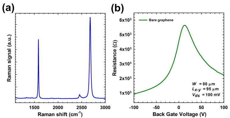
Raman spectroscopy was used to confirm the layer number of graphene film. In the Raman spectrum shown in Figure 4a, the G-peak (~1600 cm−1) and 2D-peak (~2700 cm−1) are clearly resolved with strong intensity and sharp shape of 2D peak, indicating that the graphene film is monolayer. To avoid possible surface contaminations, all devices were thermal-annealed (Ar 1.5 ccm and H2 250 sccm, 300 K) before electrical measurements were performed. Figure 4b presents the back gate (Vback·gate)-dependent resistance measurement results of a typical graphene FET device, showing the ambipolar field-effect characteristics. Both the carrier type and density of graphene can be modulated by Vback·gate. The maximum resistance (or the minimal conductance) point corresponds to the charge neutrality point Vcnp (or the Dirac point in the case of monolayer graphene), indicating how the graphene film is intrinsically doped, i.e., p/n doped when Vcnp is positive/negative or non-doped when Vcnp is equal to zero. For this particular device, Vcnp is around 12 V, suggesting it is intrinsically p-doped. The p-doping characteristics of graphene are usually caused by exposure to an oxygen-containing atmosphere, as oxygen molecules adsorbed onto defect or oxidized sites on a graphene surface will function as p-type dopants by trapping electrons during device fabrication process [26]. Several studies have shown that the conductance of graphene device exhibited ambipolar behavior and demonstrated better operating stability and higher sensing performance in the p-type region than in the n-type region [27,28]. The slight asymmetry around the Dirac point can be ascribed to the interaction of graphene with the contacts, as explained by Di Bartolomeo et al. [29,30].The feature of being sensitive to the surrounding environment renders graphene an ideal sensing material for detecting charged objects. With the presence of certain charged environment, the charge doping level (or Fermi level) of graphene will be changed, resulting in a shift of Vcnp or the resistance-Vback·gate curve.
Figure 4.
Raman characterization of patterned graphene channel (a) and resistance-back gate voltage curve of a typical graphene FET device (b).
3.3. Dependence of hCG Concentration
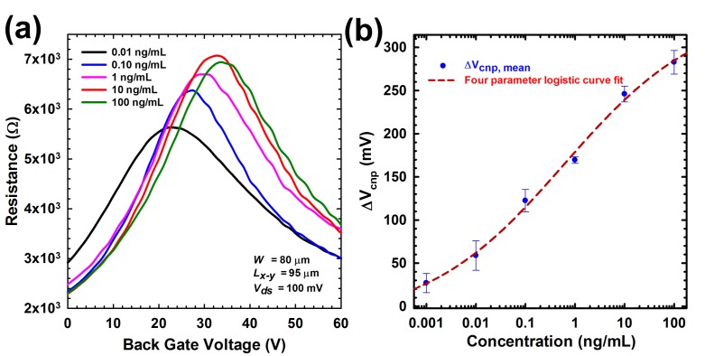
To examine the performance of bgFET immunosensor for detection, we performed a quantitative analysis on multiple BG-gFET devices to examine the change in resistance of the graphene channel after Ab-hCG binding ranging from 1 pg·mL−1 to 100 ng·mL−1. All the devices were formed by modification processes under controlled physiochemical conditions. We used 100 µg·L−1 PBS to obtain standard solutions with different concentrations. After adding standard solutions with different concentrations for four hours at 4 °C followed by washing with PBS and N2 drying, we measured the resistance-Vback·gate curves within 2 min. The pH of standard solutions was kept at neutral to avoid false response. At least three replicates were conducted for each concentration and the relative standard deviations between replicates were 5%–24%, indicating good reproducibility of our measurement. The test results of standard solutions with five concentrations (i.e., 1 pg·mL−1, 10 pg·mL−1, 100 pg·mL−1, 1 ng·mL−1, 100 ng·mL−1) are shown in Figure 5a. Before adding solutions, the Vcnp was around 12 V, indicating the p-doping nature of the device in dry state. After adding standard solution of 1 pg·mL−1, we clearly observed right shifts of the curve, i.e., higher Vcnp. For higher concentrations, the resistance-Vback·gate shifted further right and Vcnp became higher.
Figure 5.
(a) The resistance-Vback·gate curves of five different hCG concentrations (1 pg·mL−1~100 ng·mL−1). (b) The measured ΔVcnp versus concentration (in semilog scale); The red dotted line corresponds to the fitting results by using a four parameter logistic function.
Such results indicate that our bgFET immunosensors are effective for detecting at different concentrations. The detection mechanism can be explained by a simple picture that, in dry condition, higher concentrations of hCG cause electron doping of the graphene (which is intrinsically p-doped) by approaching its surface, which leads to a right shift of the transfer curves or a higher Vcnp [31] and potentially used as an effective parameter to characterize ion concentrations. We tested multiple devices with similar response observed. In Figure 5b, we plotted the measured ∆Vcnp versus concentration (in logarithmic scale) of the tested standard solutions from three representative devices. A lognormal fitting was performed to obtain a calibration curve for quantification. Based on our measurement, the lowest concentration our graphene aptasensor detected was 1 pg·mL−1, and a concentration-response calibration curve showed a good fitting (R2 = 0.97) in the range of concentration evaluated, which is advantageous for the detection of hCG having wide-ranging expression profiles in the different stages of diagnosis i.e., pregnancy or cancer development. The obtained limit of detection (LOD) was 600 times more sensitive than the one achieved with the previously published hCG biosensor on BG-gFET [15] and twenty times better than one obtained with polysilicon nanogap [32]. In addition, our biosensor was capable of clearly monitoring the anti-hCG + hCG interaction at concentration as low as 1 pg·mL−1 directly without pre- or post-amplification process. This demonstrated that our aptasensor can work well for samples much lower than the safe level.
3.4. Slectivity, Stability, Reproducibility and Reusability
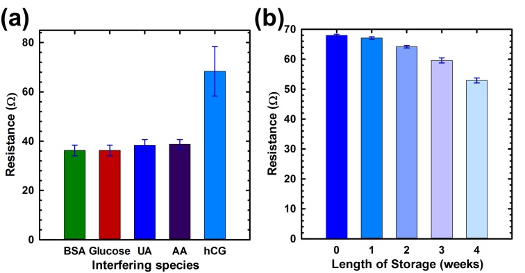
Selectivity tests were carried out by using interfering species, such as BSA, glucose, uric acid (UA), ascorbic acid (AA) and 1 pg/mL of hCG (Figure 6a). It can be observed that the response of interfering species on our BG-gFET is less than 40 mV at the lowest concentration of hCG. In addition, the BG-gFETs showed satisfactory stability. After a month long storage, the resistance response decreased 21%, which is due to the gradual deactivation of the immobilized biomolecules (Figure 6b). At present, the sensor is for one-time use only, however, to extend the BG-gFET sensor into practical reusable applications, further work is needed.
Figure 6.
Selectivity and stability measurements for BG-gFET immunosensor. (a) The selectivity of the immunosensor with interfering species. BSA, Glucose (GLUC), Uric Acid (UA) and Ascorbic Acid (AA) were used; (b) long term stability of the biosensor for upto four weeks of storage.
4. Conclusions
In summary, we demonstrated a BG-gFET based immunosensor functionalized with a non-covalent linker for high sensitivity and label-free detection of hCG. The sensors showed the detection of hCG at concentration levels as low as 1 pg·mL−1, which is much lower than the clinical limit (5 ng·mL−1) with a broad dynamic range in concentration (1 pg·mL−1 to 100 ng·mL−1) [15]. Further development in multiple markers with a multiplex array is necessary for scalable and cost-effective detection. These results clearly show that BG-gFET immunosensors are promising devices for the use as label-free biological sensors that can electrically detect biomolecules.
Acknowledgments
We gratefully acknowledge financial support from the Engineering and Physical Sciences Research Council (EPSRC, Swindon, UK) through its Programme Grant scheme (Grant No. EP/M006301/1). We also acknowledge the technical support on annealing from Professor Guy’s group at Swansea University and XPS from the National EPSRC XPS Users’ Service (Newcastle University).
Author Contributions
K.I. and G.P. conceived and designed the experiments; K.I. performed the experiments; K.I. and A.S. analyzed the data; K.I. and G.P. contributed analysis tools; K.I. and G.P. co-wrote the paper.
Conflicts of Interest
The authors declare no conflict of interest.
References
- 1.Chetcuti A.F., Wong D.K., Stuart M.C. An indirect perfluorosulfonated ionomer-coated electrochemical immunosensor for the detection of the protein human chorionic gonadotrophin. Anal. Chem. 1999;71:4088–4094. doi: 10.1021/ac981216a. [DOI] [PubMed] [Google Scholar]
- 2.Stenman U.-H., Tiitinen A., Alfthan H., Valmu L. The classification, functions and clinical use of different isoforms of HCG. Hum. Reprod. Update. 2006;12:769–784. doi: 10.1093/humupd/dml029. [DOI] [PubMed] [Google Scholar]
- 3.Chai R., Yuan R., Chai Y., Ou C., Cao S., Li X. Amperometric immunosensors based on layer-by-layer assembly of gold nanoparticles and methylene blue on thiourea modified glassy carbon electrode for determination of human chorionic gonadotrophin. Talanta. 2008;74:1330–1336. doi: 10.1016/j.talanta.2007.08.046. [DOI] [PubMed] [Google Scholar]
- 4.Zhang B., Mao Q., Zhang X., Jiang T., Chen M., Yu F., Fu W. A novel piezoelectric quartz micro-array immunosensor based on self-assembled monolayer for determination of human chorionic gonadotropin. Biosens. Bioelectron. 2004;19:711–720. doi: 10.1016/S0956-5663(03)00260-4. [DOI] [PubMed] [Google Scholar]
- 5.Wang J., Yuan R., Chai Y., Cao S., Guan S., Fu P., Min L. A novel immunosensor based on gold nanoparticles and poly-(2,6-pyridinediamine)/multiwall carbon nanotubes composite for immunoassay of human chorionic gonadotrophin. Biochem. Eng. J. 2010;51:95–101. doi: 10.1016/j.bej.2010.05.005. [DOI] [Google Scholar]
- 6.Vartiainen J., Alfthan H., Lehtovirta P., Stenman U.H. Elevated hCG and a high proportion of hCGβ in serum preceding the diagnosis of trophoblastic disease by seven months. BJOG Int. J. Obstet. Gynaecol. 2002;109:589–590. doi: 10.1016/S1470-0328(02)00195-7. [DOI] [PubMed] [Google Scholar]
- 7.Wen G., Liang X., Liu Q., Liang A., Jiang Z. A novel nanocatalytic sers detection of trace human chorionic gonadotropin using labeled-free vitoria blue 4R as molecular probe. Biosens. Bioelectron. 2016;85:450–456. doi: 10.1016/j.bios.2016.05.024. [DOI] [PubMed] [Google Scholar]
- 8.Bergveld P. Development, operation, and application of the ion-sensitive field-effect transistor as a tool for electrophysiology. IEEE Trans. Biomed. Eng. 1972:342–351. doi: 10.1109/TBME.1972.324137. [DOI] [PubMed] [Google Scholar]
- 9.De Moraes A.C.M., Kubota L.T. Recent trends in field-effect transistors-based immunosensors. Chemosensors. 2016;4:20. doi: 10.3390/chemosensors4040020. [DOI] [Google Scholar]
- 10.Novoselov K.S., Geim A.K., Morozov S.V., Jiang D., Zhang Y., Dubonos S.V., Grigorieva I.V., Firsov A.A. Electric field effect in atomically thin carbon films. Science. 2004;306:666–669. doi: 10.1126/science.1102896. [DOI] [PubMed] [Google Scholar]
- 11.Pumera M. Graphene in biosensing. Mater. Today. 2011;14:308–315. doi: 10.1016/S1369-7021(11)70160-2. [DOI] [Google Scholar]
- 12.Kuila T., Bose S., Khanra P., Mishra A.K., Kim N.H., Lee J.H. Recent advances in graphene-based biosensors. Biosens. Bioelectron. 2011;26:4637–4648. doi: 10.1016/j.bios.2011.05.039. [DOI] [PubMed] [Google Scholar]
- 13.Mohanty N., Berry V. Graphene-based single-bacterium resolution biodevice and DNA transistor: Interfacing graphene derivatives with nanoscale and microscale biocomponents. Nano Lett. 2008;8:4469–4476. doi: 10.1021/nl802412n. [DOI] [PubMed] [Google Scholar]
- 14.Liu F., Kim Y.H., Cheon D.S., Seo T.S. Micropatterned reduced graphene oxide based field-effect transistor for real-time virus detection. Sens. Actuators B Chem. 2013;186:252–257. doi: 10.1016/j.snb.2013.05.097. [DOI] [Google Scholar]
- 15.Teixeira S., Burwell G., Castaing A., Gonzalez D., Conlan R., Guy O. Epitaxial graphene immunosensor for human chorionic gonadotropin. Sens. Actuators B Chem. 2014;190:723–729. doi: 10.1016/j.snb.2013.09.019. [DOI] [Google Scholar]
- 16.Yeh C.-H., Kumar V., Moyano D.R., Wen S.-H., Parashar V., Hsiao S.-H., Srivastava A., Saxena P.S., Huang K.-P., Chang C.-C., et al. High-performance and high-sensitivity applications of graphene transistors with self-assembled monolayers. Biosens. Bioelectron. 2016;77:1008–1015. doi: 10.1016/j.bios.2015.10.078. [DOI] [PubMed] [Google Scholar]
- 17.Ping J., Vishnubhotla R., Vrudhula A., Johnson A.C. Scalable production of high-sensitivity, label-free DNA biosensors based on back-gated graphene field effect transistors. ACS Nano. 2016;10:8700–8704. doi: 10.1021/acsnano.6b04110. [DOI] [PMC free article] [PubMed] [Google Scholar]
- 18.Gao Z., Kang H., Naylor C.H., Streller F., Ducos P., Serrano M.D., Ping J., Zauberman J., Carpick R.W., Wang Y.-J., et al. Scalable production of sensor arrays based on high-mobility hybrid graphene field effect transistors. ACS Appl. Mater. Interfaces. 2016;8:27546–27552. doi: 10.1021/acsami.6b09238. [DOI] [PubMed] [Google Scholar]
- 19.Li B., Pan G., Suhail A., Islam K., Avent N., Davey P. Deep UV hardening of photoresist for shaping of graphene and lift-off fabrication of back-gated field effect biosensors by ion-milling and sputter deposition. Carbon. 2017;118:43–49. doi: 10.1016/j.carbon.2017.03.032. [DOI] [Google Scholar]
- 20.Li X., Cai W., An J., Kim S., Nah J., Yang D., Piner R., Velamakanni A., Jung I., Tutuc E., et al. Large-area synthesis of high-quality and uniform graphene films on copper foils. Science. 2009;324:1312–1314. doi: 10.1126/science.1171245. [DOI] [PubMed] [Google Scholar]
- 21.Suk J.W., Kitt A., Magnuson C.W., Hao Y., Ahmed S., An J., Swan A.K., Goldberg B.B., Ruoff R.S. Transfer of CVD-grown monolayer graphene onto arbitrary substrates. ACS Nano. 2011;5:6916–6924. doi: 10.1021/nn201207c. [DOI] [PubMed] [Google Scholar]
- 22.Islam K., Chand R., Han D., Shin I.-S., Kim Y.-S. An electrochemical assay for restriction endonuclease activity using graphene monolayer. J. Electrochem. Soc. 2014;161:B261–B264. doi: 10.1149/2.0621412jes. [DOI] [Google Scholar]
- 23.Suhail A., Islam K., Li B., Jenkins D., Pan G. Reduction of polymer residue on wet–transferred cvd graphene surface by deep UV exposure. Appl. Phys. Lett. 2017;110:183103. doi: 10.1063/1.4983185. [DOI] [Google Scholar]
- 24.Li B., Pan G., Jamil N.Y., Al Taan L., Awan S., Avent N. Shielding technique for deposition of au electrical contacts on graphene by sputtering. J. Vac. Sci. Technol. A. 2015;33:030601. doi: 10.1116/1.4916589. [DOI] [Google Scholar]
- 25.Vuoriluoto M., Orelma H., Zhu B., Johansson L.-S., Rojas O.J. Control of protein affinity of bioactive nanocellulose and passivation using engineered block and random copolymers. ACS Appl. Mater. Interfaces. 2016;8:5668–5678. doi: 10.1021/acsami.5b11737. [DOI] [PubMed] [Google Scholar]
- 26.Schedin F., Geim A., Morozov S., Hill E., Blake P., Katsnelson M., Novoselov K. Detection of individual gas molecules adsorbed on graphene. Nat. Mater. 2007;6:652–655. doi: 10.1038/nmat1967. [DOI] [PubMed] [Google Scholar]
- 27.Park S.J., Kwon O.S., Lee S.H., Song H.S., Park T.H., Jang J. Ultrasensitive flexible graphene based field-effect transistor (fet)-type bioelectronic nose. Nano Lett. 2012;12:5082–5090. doi: 10.1021/nl301714x. [DOI] [PubMed] [Google Scholar]
- 28.Kwon O.S., Park S.J., Hong J.-Y., Han A.-R., Lee J.S., Lee J.S., Oh J.H., Jang J. Flexible fet-type vegf aptasensor based on nitrogen-doped graphene converted from conducting polymer. ACS Nano. 2012;6:1486–1493. doi: 10.1021/nn204395n. [DOI] [PubMed] [Google Scholar]
- 29.Di Bartolomeo A., Giubileo F., Romeo F., Sabatino P., Carapella G., Iemmo L., Schroeder T., Lupina G. Graphene field effect transistors with niobium contacts and asymmetric transfer characteristics. Nanotechnology. 2015;26:475202. doi: 10.1088/0957-4484/26/47/475202. [DOI] [PubMed] [Google Scholar]
- 30.Di Bartolomeo A., Santandrea S., Giubileo F., Romeo F., Petrosino M., Citro R., Barbara P., Lupina G., Schroeder T., Rubino A. Effect of back-gate on contact resistance and on channel conductance in graphene-based field-effect transistors. Diam. Relat. Mater. 2013;38:19–23. doi: 10.1016/j.diamond.2013.06.002. [DOI] [Google Scholar]
- 31.Khan M.F., Iqbal M.Z., Iqbal M.W., Iermolenko V.M., Khalil H.W., Nam J., Kim K.S., Noh H., Eom J. Stable and reversible doping of graphene by using KNO3 solution and photo-desorption current response. RSC Adv. 2015;5:50040–50046. doi: 10.1039/C5RA08136J. [DOI] [Google Scholar]
- 32.Balakrishnan S., Hashim U., Gopinath S.C., Poopalan P., Ramayya H., Omar M.I., Haarindraprasad R., Veeradasan P. A point-of-care immunosensor for human chorionic gonadotropin in clinical urine samples using a cuneated polysilicon nanogap lab-on-chip. PLoS ONE. 2015;10:e0137891. doi: 10.1371/journal.pone.0137891. [DOI] [PMC free article] [PubMed] [Google Scholar]


