

A metallic trench Fabry-Perot resonator achieves room temperature lasing of surface plasmons with a record-narrow linewidth.
Abstract
Recent years have witnessed a growing interest in the development of small-footprint lasers for potential applications in small-volume sensing and on-chip optical communications. Surface plasmons—electromagnetic modes evanescently confined to metal-dielectric interfaces—offer an effective route to achieving lasing at nanometer-scale dimensions when resonantly amplified in contact with a gain medium. We achieve narrow-linewidth visible-frequency lasing at room temperature by leveraging surface plasmons propagating in an open Fabry-Perot cavity formed by a flat metal surface coated with a subwavelength-thick layer of optically pumped gain medium and orthogonally bound by a pair of flat metal sidewalls. We show how the lasing threshold and linewidth can be lowered by incorporating a low-profile tapered grating on the cavity floor to couple the excitation beam into a pump surface plasmon polariton providing a strong modal overlap with the gain medium. Low-perturbation transmission-configuration sampling of the lasing plasmon mode is achieved via an evanescently coupled recessed nanoslit, opening the way to high–figure of merit refractive index sensing of analytes interacting with the open metallic trench.
INTRODUCTION
Ongoing miniaturization of the footprint of optical systems and circuits requires development of wavelength scale optical elements able to efficiently generate, manipulate, and detect light. Achieving coherent optical sources with narrow linewidth and nanoscale mode confinement in one or more dimensions has been central to this quest (1). Nanolasers incorporating high-index dielectric resonators under the form of photonic crystals (2–4) or whispering-gallery mode cavities (5–7) have constituted a major focus of research over the past few decades. More recently, metal-based resonators that sustain surface plasmons have emerged as a promising route to achieving stimulated emission (8–10) or lasing (11–20) at nanometer-scale dimensions. For example, optically pumped lasing plasmon modes formed by localized surface plasmons on dye-coated resonant nanoparticles and nanoparticle arrays (11–13), or by gap plasmons confined to a dielectric layer of nanoscale thickness between a metal surface and a semiconductor gain medium (14–19), have been recently demonstrated.
Here, we show lasing of propagating surface plasmon polaritons (SPPs) confined to an open Fabry-Perot cavity. Visible-frequency lasing is achieved at room temperature with record-narrow linewidth for any plasmon laser reported to date. The cavity consists of a template-stripped ultrasmooth flat Ag surface orthogonally bound by a pair of Ag sidewalls, forming a trench-shaped, micrometer-scale width resonator for SPPs exhibiting a record-high quality factor, and a figure of merit for refractive index sensing that is an order of magnitude higher than that of a state-of-the-art surface plasmon resonance (SPR) sensor (21, 22). By incorporating a dye-doped polymer film of subwavelength thickness on the trench floor and optically pumping the dye from the open side of the cavity, we demonstrate room temperature SPP lasing in the red. We show how the lasing threshold and linewidth can be lowered by incorporating a low-profile tapered grating on the cavity floor to couple the excitation beam into a pump SPP providing a strong modal overlap with the gain medium. The record-narrow lasing linewidth (≈0.24 nm) achieved here is substantially narrower than that of localized plasmon lasers (11–13) and comparable to that of the best semiconductor-based gap plasmon laser (16, 17) demonstrated to date. Transmission-configuration sampling of the lasing intensity with minimum perturbation to both the pump and emission SPPs is achieved via an evanescently coupled nanoslit recessed below the cavity floor, opening the way to potential applications in small-volume optical sensing.
RESULTS
SPP Fabry-Perot resonator
A flat surface of noble metal facing a dielectric medium forms a canonical medium for sustaining SPPs—transverse-magnetic (TM)–polarized electromagnetic waves that propagate along the interface and evanescently decay normal to the interface, both into the metal (typically on a deep-subwavelength scale) and into the dielectric (typically on the scale of a wavelength). The rectangular open-trench structure conceived here to form the optical resonator of a visible-frequency SPP laser is defined by a planar, optically opaque Ag “floor”—delimited by two optically opaque, quasi-planar, quasi-parallel Ag “sidewalls,” oriented normal to the floor (Fig. 1A). White-light illumination of the cavity launches SPPs along the metal-air interface of the floor via scattering at the sidewall-floor corners. These SPPs, in turn, propagate across the cavity and reflect efficiently from the sidewalls, which act like SPP mirrors (23, 24). The cavity can sustain resonance of SPP modes propagating normal to the mirrors (in the x direction), where mirror separation l corresponds to an integer number of SPP half wavelengths. The rectangular profile of the resonant cavity allows for SPP standing waves of arbitrary extent parallel to the mirrors (along the y direction). To avoid scattering losses of the SPP field at the top corner of the cavity, the sidewall mirror height h is chosen to exceed SPP decay length normal to the cavity floor (in the z direction). A slit fabricated in the cavity floor, of subwavelength width (in the x direction) and arbitrary length (in the y direction), evanescently connects the cavity to a transparent substrate situated on its reverse side, which allows the transmission mode probing of cavity SPP modes close to their plane of maximum intensity at the metal surface. Orienting the slit parallel to the cavity sidewalls—that is, parallel to the magnetic field vector of the SPP standing wave—allows efficient coupling between the SPP field in the cavity and the TM-polarized fundamental propagating mode of the slit.
Fig. 1. Design, fabrication, and characterization of the metallic trench SPP Fabry-Perot resonator.
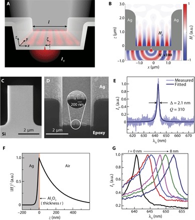
(A) Schematic diagram of a plasmonic trench resonator, consisting of an opaque Ag film forming two vertical Ag sidewalls (separation l) and a horizontal floor and illuminated with white light from free space. The schematic standing wave (red) illustrates the trapping of a resonant SPP mode. A recessed subwavelength-width slit, offset from the cavity center by distance ζ, evanescently samples the resonant SPP mode and transmits a wave of proportional intensity, IT, into the far field via a transparent substrate. (B) Finite-difference time-domain (FDTD) simulated normalized Hy-field distribution at λ0 = 647 nm assuming a cavity length of l = 2.5 μm and a vertical mirror height of h = 2 μm, along with a sampling slit (slit-sidewall taper angle = 15°, δ = 50 nm, and σ = 10 nm) positioned at ζ = 465 nm. For ease of visualization, Hy is multiplied by 100 in the plane below the cup floor (z < 0). The slit samples a small fraction of the time-varying electromagnetic field at the surface of the cavity floor by coupling to the x-directed electric field component of the SPP standing wave, also minimal at this position, converting it into a guided mode, and radiating it into the far field on the back side of the cavity. (C) Scanning electron microscope (SEM) image of the silicon mesa used for the template-stripping method to fabricate the resonator with a sidewall height of h = 3 μm and sidewall taper angles of ≤0.2°. (D) SEM image of the focused ion beam (FIB) cross section of the fabricated resonator, exposing the profile of the fabricated recessed slit underneath the cavity floor. Inset: Magnified view of the cross section of the recessed slit with an ultranarrow slit end width of σ ≈ 10 nm and a natural slit sidewall taper angle of ≈5°. (E) Measured spectrum of the transmitted light intensity outcoupled by the slit aperture IT under illumination of the open side of the cavity with incoherent white light. The measured spectrum was fitted with a Lorentzian shape to estimate the linewidth Δ and quality factor Q. (F) FDTD-simulated cross section of the magnetic field intensity |Hy(z)|2 at the center of the cavity (ζ = 0 nm), for a cavity coated with a layer of Al2O3 of a thickness of t = 8 nm and illuminated at λ0 = 653 nm. (G) Experimentally measured transmission spectra of the cavity resonator described in (D) successively coated with Al2O3 layers of increasing thickness from 0 to 8 nm, displayed in thickness increments of 1.6 nm. a.u., arbitrary units.
The quality factor of the cavity resonator, limited by the round-trip loss of the trapped SPP mode, can be maximized by (i) minimizing the propagation loss of the SPPs along the cavity floor (section S1), (ii) minimizing the SPP reflection losses at each of the metal sidewalls (section S2), (iii) optimizing the length of the Fabry-Perot cavity l (section S3), and (iv) minimizing the scattering loss from the recessed sampling slit (section S4). The FDTD simulated magnetic field Hy of a slit-decorated cavity at resonance (λ0 = 647 nm, Fig. 1B), optimized according to the above criteria, is characterized by a laterally trapped SPP standing wave in the cavity, evanescently decaying normal to the cavity floor, and for which one of the magnetic field nodes coincides with the location of the recessed slit. The spectrum of the transmitted intensity, monitored at a distance of 500 nm below the exit aperture of the slit, reveals a cavity mode with a resonance characterized by a peak position of λpeak = 647 nm and a full-width half-maximum (FWHM) linewidth of Δ = 1.8 nm, corresponding to a high quality factor of Q = λpeak/Δ = 360.
Fabrication of the optimized cavity resonator (section S5) is performed using the template-stripping method (25). The pattern template consists of a reusable, high–aspect ratio Si mesa (Fig. 1C) having a flat, ultrasmooth top surface, along with sidewalls that are orthogonal to within an angular tolerance of ≤0.2°, over a vertical distance of ≈3 μm from the top surface. Silver is angle-evaporated onto the Si template, to top-surface and sidewall thicknesses of ≈300 and ≈250 nm, respectively. A slit with a nominal lateral slit offset of 155 nm relative to the center of the mesa is then patterned through the top-surface Ag film via low-current FIB milling, stopping short of the Ag-Si interface by a recess distance of δ ≈ 50 nm. Template stripping then yields an open, high–aspect ratio cavity (Fig. 1D) having features that conspire to minimize SPP propagation and scattering losses, namely, a recessed sampling slit, an ultrasmooth Ag surface for the cavity floor, and quasi-vertical Ag sidewalls.
The optical properties of the fabricated SPP resonator are characterized by illuminating the open side of the cavity with incoherent white light, collecting the light transmitted through the slit using an inverted optical microscope, and dispersing the collected light onto a grating spectrometer. The resulting spectrum of the collected intensity IT reveals a pronounced resonance peak centered at λpeak = 642 nm and characterized by a linewidth of Δ = 2.1 ± 0.1 nm (Fig. 1E). The uncertainty in the measurement of the resonance linewidth is 1 SD of the Lorentzian fit parameter. To our knowledge, the resulting Q = 310 ± 15 is the largest quality factor directly measured to date for a resonator using only SPPs. The uncertainty in the calculated Q is 1 SD based on propagation of uncertainty from the resonance linewidth curve fitting.
To evaluate the performance of a refractive index sensor based on the plasmonic trench resonator, we expose the cavity floor to a superficial perturbation in the index of refraction under the form of ultrathin Al2O3 layers of an index of n = 1.77 of thickness ranging from 0.8 to 8 nm, conformally deposited using atomic layer deposition. The simulated surface magnetic field intensity, |Hy|2, at the center of the cavity depicting the exponential decay of the SPP mode into the Ag film (y < 0) and into the space above the Ag film (y > 0), is illustrated in Fig. 1F in the case of an 8-nm-thick layer of Al2O3. Nanometer-scale spectral shifts to longer wavelengths of the peak position of the resonance, λpeak, are easily resolvable as a function of increasing layer thickness because of the relatively narrow resonance linewidths (Fig. 1G). On the basis of an analytic treatment of an SPP mode propagating along a Ag surface coated with a layer of Al2O3 of thickness t, the dependence of λpeak on t can be shown to be equivalent to a bulk-index sensitivity of S = dλpeak/dneff ≈ 714 nm·RIU−1 (where neff is the refractive index of a bulk dielectric medium facing the Ag surface). For the minimum observed cavity resonance linewidth of Δ = 2.1 nm (Fig. 1E), the calculated figure of merit is FOM = S/Δ = 340, which is a factor of 10 higher than that of a state-of-the-art, commercial SPR sensor based on Kretschmann configuration excitation (21, 22).
SPP Fabry-Perot laser
On the basis of the optimized design of a rectangular-cavity SPP resonator, we implement a laser based on stimulated amplified emission of SPPs by incorporating a thin layer of solid-state gain medium into the open-trench structure and shifting the recessed slit position to a new position ζ′ = 55 nm (Fig. 2A). The gain medium consists of a host medium of polymethyl methacralate (PMMA) doped with 4-(dicyanomethylene)-2-methyl-6-(4-dimethylaminostyryl)-4H-pyran (DCM) laser dye to a concentration of 3 mM with a minimum thickness of ≈260 nm at the center of the cavity floor (Fig. 2B, inset). The PMMA:DCM gain medium absorbs photons with a maximum absorption efficiency at λP = 480 nm, emits light in a wavelength range of 560 nm ≲ λE ≲ 715 nm, with a maximum at 610 nm (section S6), and has been shown to provide a large gain coefficient (26, 27).
Fig. 2. Experimental characterization of the SPP Fabry-Perot laser.
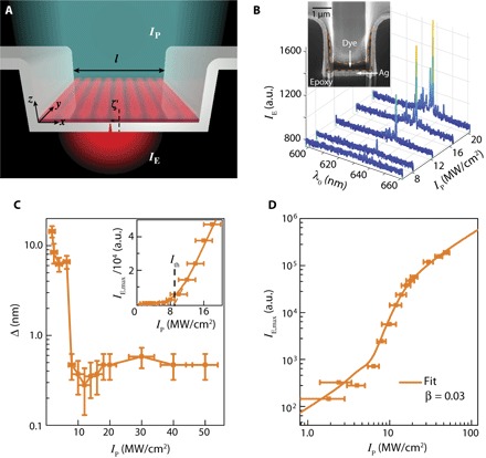
(A) Schematic diagram of the metallic trench SPP laser, consisting of a gain medium–decorated Fabry-Perot resonator, illuminated with a pump beam (blue-green) of intensity IP. The schematic standing wave (red) illustrates a trapped SPP lasing mode. A recessed slit, offset from the cavity center by distance ζ′, evanescently samples the lasing SPP mode and transmits a wave of proportional intensity, IE, into the far field. (B) Evolution of the spectrum of IE with increasing pump intensity IP. Inset: SEM image of the FIB cross section of the fabricated SPP laser. A thin layer of platinum was deposited on top of the device to assist with the FIB cross section. The orange dashes outline the boundaries of the spin-coated gain medium. (C) Emission linewidth, Δ, and (D) log scale light-light curve of the outcoupled light emission, IE, versus IP. The uncertainties in the measurements of IP are 1 SD based on the measurement of pump energy from 100 consecutive pulses. (C) Inset: IE versus IP on a linear scale indicating the lasing threshold Ith.
The resulting device is optically characterized at room temperature by pumping its open side with a normally incident-tunable nanosecond-pulsed laser (λP = 480 nm) and spectrally characterizing the intensity transmitted by the slit, IE, which is proportional to the intensity of the emitted cavity SPPs. The evolution of distinct spectral emission peaks as a function of pump intensity IP hints at the possibility of SPP lasing (Fig. 2B). Note that the light sampled by the slit cannot correspond to any nonplasmonic lasing modes, which would be characterized by a field minimum at the metal surface. The hypothesis of lasing is substantiated by the observed dependence of emission linewidth Δ (Fig. 2C) and intensity IE,max (Fig. 2C, inset), respectively, of the prominent spectral peak at λE ≈ 637 nm. Specifically, the evolution of the emission intensity, displaying a canonical “kink” shape on a log-log scale (Fig. 2D), is consistent with three distinct emission regimes characteristic of a standard laser as it transitions through threshold: (i) spontaneous emission for IP ≲ 4.0 MW/cm2, (ii) amplified spontaneous emission for 4.0 MW/cm2 ≲ IP ≲ 12.0 MW/cm2, coinciding with a rapid increase in the emission intensity, and (iii) stimulated emission for IP ≳ 12.0 MW/cm2. In particular, the variation of experimental emission intensity versus IP (Fig. 2D) is amenable to a close fit to a solution of the rate equation, yielding a spontaneous emission factor of β = 0.03 ± 0.01 and a laser threshold intensity of Ith = 8.8 ± 1.2 MW/cm2 (section S7). The uncertainties in β and Ith are 1 SD of the nonlinear fit parameters of the measured data to the laser rate equation. Moreover, the emission linewidth rapidly decreases as a function of increasing IP, reaching a minimum value of Δ = 0.28 ± 0.15 nm and further remaining relatively constant for higher values of IP. The uncertainty in the measurement of the resonance linewidth is 1 SD of the Lorentzian fit parameter. Further evidence to support lasing behavior of the dye-coated SPP cavity resonator is provided by consistency with predictions of FDTD simulations exploiting a four-level model for the gain medium (section S8).
Grating-decorated SPP-pumped SPP laser
Optimizing the absorption efficiency of a free-space pump beam by the gain medium used in plasmon amplifiers and lasers, without simultaneously introducing significant loss channels for the amplified/lasing surface plasmon modes, remains a challenging problem (28, 29). In particular, the pumping of an SPP traveling within a gain medium along a metal surface is fundamentally inefficient when using free-space illumination, due to poor mode overlap in the direction normal to the surface between the evanescently decaying SPP, which has an intensity maximum at the surface, and the standing wave resulting from free-space pumping, which has an intensity minimum at that surface (28). One demonstrated approach to increasing the interaction between a pump and a signal SPP mediated by a nonlinear medium involves providing the pump under the form of an SPP that propagates along the same metal surface (30, 31). Here, we improve the absorption of the pump by the thin-film gain medium and increase gain-mode overlap between the pump and the SPP by converting a normally incident free-space pump beam into surface plasmon waves confined to the cavity floor (“pump SPPs”), leading to an SPP laser with a substantially lowered lasing threshold. This is achieved by leveraging a low-profile, sinusoidal grating added onto the cavity floor to couple an excitation beam polarized orthogonal to the grating into counterpropagating SPPs, forming a pump SPP standing wave directly generated inside the lasing cavity (Fig. 3A). To maximize the coupling of the excitation beam at normal incidence, the grating periodicity p is chosen to nominally match the pump-SPP effective wavelength λP/nSPP (where the SPP mode index nSPP versus the free-space wavelength is shown in section S9). To limit out-of-plane diffraction of the resulting lasing SPPs by the same grating, we oriented the grating ridges parallel to the propagation direction of the lasing SPPs (along the x direction, normal to the sidewall mirrors), thus resulting in orthogonal standing waves for lasing SPPs and pump SPPs, respectively. In addition, the grating is designed to only partially occupy the full cavity width (along the x direction), leaving flat cavity floor “buffer” segments adjacent to either mirror, which (i) can accommodate, as demonstrated earlier, straightforward integration of a subsurface sampling slit having a well-controlled, constant recess δ below the cavity floor and (ii) act to protect the flatness of the sidewall mirrors during the modified template-stripping fabrication process described subsequently. To minimize reflection/scattering of the lasing SPPs at the boundaries between the grating and flat regions and provide adiabatic mode transition between the respective regions, we modulated the grating height along the x direction by one period of a cosine function, yielding a gently tapered profile toward each side of the cavity (Fig. 3A).
Fig. 3. Experimental characterization of grating-decorated SPP-pumped SPP laser.
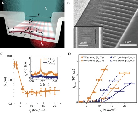
(A) Schematic diagram of an SPP laser decorated with a low-profile grating of periodicity p, peak height d with respect to cavity floor, and offset ξ from the cavity center, illuminated with a pump beam (blue-green) of intensity IP. The schematic blue-green and red standing waves illustrate the grating-coupled pump SPPs and cavity-trapped lasing SPPs, respectively. A recessed slit, offset from the cavity center by distance ζ″, evanescently samples the lasing SPP mode and transmits a wave of proportional intensity, IE, into the far field. (B) Tilted-view SEM image of the template-stripped cavity resonator illustrating the grating-decorated cavity floor. Inset: Top-view SEM image of the device, where the nominal location of the buried recessed sampling slit is indicated by the dotted black line. (C) Evolution of the SPP emission linewidth Δ with increasing pump intensity IP. Inset: Representative emission spectra of IE for IP below (IP = 4.0 MW/cm2) and above (IP = 6.0 MW/cm2) the lasing threshold (Ith = 5.6 MW/cm2). (D) SPP lasing turn-on characteristics IE versus IP on a linear scale for grating-decorated and grating-free devices as a function of in-plane pump polarization.
The proposed SPP-pumped SPP laser is fabricated using a modified template-stripping process in which the Si mesa is patterned to simultaneously mold the Fabry-Perot cavity and the tapered coupling grating on the cavity floor (see Materials and Methods). The fabrication process, including the FIB milling of the sampling slit before template stripping, yields a Ag-coated rectangular cavity of a width of l′ = 4.4 μm (Fig. 3B) that features a tapered grating on the cavity floor having a peak height of d = 40 nm (section S10), a periodicity of p = 350 nm, and a length of 30 μm in the direction parallel to the sidewalls (y direction; Fig. 3B, inset), as well as a width of w = 3 μm in the direction normal to the sidewalls (x direction) with a lateral offset of ξ = 320 nm. The recessed sampling slit (Fig. 3B, inset) is positioned within the larger of the two flat buffer areas, at a lateral offset of ζ = 1.5 μm with respect to the cavity center. The fabrication of the SPP-pumped SPP laser is finalized by incorporating a PMMA:DCM gain medium of dye concentration and nominal thickness identical to that of the free-space pumped SPP laser described in Fig. 2. For reference, laser structures having different grating periodicities of p = 300 and 400 nm (for a chosen nominal peak height of d = 40 nm) and different peak heights of d = 20 and 80 nm (for a chosen nominal grating periodicity of p = 350 nm) were also fabricated (section S11), along with a laser structure devoid of a coupling grating.
The evolution of the SPP emission under normal-incidence, pulsed laser illumination of the structure with an excitation wavelength of λP = 480 nm and polarization orthogonal to the grating ridges (EP//y) indicates SPP lasing with a lasing threshold of Ith = 5.6 ± 1.2 MW/cm2 and a record-narrow linewidth (Δ = 0.24 ± 0.14 nm; Fig. 3C) for any room temperature plasmon laser reported to date (16). The effectiveness of grating-coupled SPP pumping in achieving low-threshold lasing is established by a comparison with a reference grating-free device of the same length illuminated under identical conditions (polarization EP//y), which displays a lasing threshold that is a factor of ≈2.1 higher (Fig. 3D; Ith = 11.6 ± 1.2 MW/cm2). The threshold reduction can be attributed to both increased gain-mode overlap due to colocation of intensity maxima of pump SPPs and lasing SPPs in the same plane at the metal surface, and net enhancement of pump absorption by a factor of 1.5 compared to the case of an unpatterned cavity floor (section S12). Note that the grating-decorated device pumped by an excitation beam polarized parallel to the grating (EP//x) similarly displays an increased lasing threshold (by a factor of ≈1.8, Ith = 10.8 ± 1.2 MW/cm2) due to the absence of any significant coupling to pump SPPs, just as in the case of the flat cavity floor. For the reference grating-free device, the lasing threshold for EP//x is also found to be lower (by a factor of ≈1.3) when compared to EP//y, because of a more efficient coupling to pump SPPs from the cavity sidewalls. Similarly, under identical illumination conditions (polarization EP//x), the lasing threshold for the grating-free device is found to be lower (by a factor of ≈1.2) than that of the grating-decorated device because the grating introduces an additional scattering loss channel for the lasing SPP.
The narrow linewidth of the SPP lasing mode of the dye-decorated Fabry-Perot resonator opens the perspective of active refractive index sensing with substantially increased figure of merit compared to that achieved using the passive resonator scheme (Fig. 1G). We theoretically evaluate this possibility by performing two-dimensional FDTD simulations of an SPP lasing mode interacting with a uniform analyte of variable index n filling the cavity above the gain medium (Fig. 4A). First, using the cavity geometry, dye composition, and dye thickness (dG = 260 nm) of the 2.5-μm-wide flat-floored SPP laser studied in section S8, along with the same pumping conditions, the lasing wavelength shift δλpeak normalized to the experimentally measured lasing linewidth of Δ = 0.24 nm (Fig. 2C) is simulated for discrete values of n varying from 1.00 to 1.02 (Fig. 4B). The slope of a linear fit to δλpeak/Δ versus n yields the figure of merit for refractive index sensing (FOM = 77.5). This value is smaller than the corresponding figure of merit simulated for a passive (dye-free) cavity of the same geometry (FOM = 352; Fig. 4B), because of the reduced SPP modal overlap with the analyte resulting from a significant fraction of the SPP mode residing within the gain medium (Fig. 4A). An increase in modal overlap can be achieved by reducing the gain medium thickness to dG = 50 nm (Fig. 4A), yielding a predicted figure of merit of 1250 (Fig. 4B) under the same pumping conditions, which is a factor of 15 higher than the highest reported to date for an active SPP sensor (19).
Fig. 4. Active refractive index sensing using the SPP lasing mode and beaming of the lasing emission.
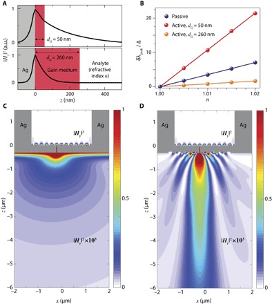
(A) FDTD-simulated cross section of magnetic field intensity |Hy(z)|2 at the center of the lasing cavity described in section S7, coated with layers of gain medium with respective thicknesses of dG = 50 nm (at λpeak = 645 nm) and 260 nm (at λpeak = 630 nm). (B) FDTD-simulated lasing wavelength shifts, δλpeak (relative to λpeak at n = 1), normalized to the corresponding experimentally measured lasing linewidth Δ = 0.24 nm (Fig. 2C), are plotted as a function of n. For reference, the simulated measured peak resonance wavelength shift (relative to λpeak at n = 1) of a passive cavity (dye-free), δλpeak, normalized to the corresponding simulated resonance linewidth Δ = 1.8 nm, is also plotted. (C) FDTD-simulated normalized magnetic field intensity distribution |Hy|2 at λE = 630 nm for the lasing cavity described in section S8 (dG = 260 nm) pumped at λP = 480 nm with an intensity of IP = 2.0 MW/cm2. For ease of visualization, |Hy|2 is multiplied by 103 in the plane below the cup floor (z < 0). (D) Same as (C), with the addition of an outcoupling beaming grating.
In addition to enabling active-mode, high-contrast refractive index sensing via the use of a thin layer of gain medium, the performance of the Fabry-Perot SPP laser as part of a larger integrated sensing system can be further optimized by enabling higher-efficiency collection of light exiting from the recessed sampling slit. For a typical far-field collection system with a numerical aperture (NA) of <1, the fraction of intercepted power is a diminishing function of the divergence of the emitted light. By decorating the surface surrounding the exit aperture of the slit with a periodic grating of subwavelength-dimension linear grooves, the divergence of the radiation pattern on the exit side of the device can be transformed from quasi-isotropic to collimated (32). This possibility is illustrated by comparing the FDTD-simulated radiation patterns (λE = 630 nm) of otherwise identical open-trench lasing structures having exit surfaces that are, respectively, (i) unpatterned (Fig. 4C) and (ii) decorated with an eight-groove grating with a pitch of 360 nm, a groove width of 180 nm, and a groove depth of 60 nm (Fig. 4D). The radiated power captured, for example, by a collection system of NA ranging from 0.75 to 0.35 is calculated to be higher by a factor ranging from 1.6 to 2.5 in the case of the grating-decorated exit surface. The ability to collimate the light sampled from the SPP laser also opens the perspective of practical collection efficiencies in lens-free integrated sensing systems that directly incorporate arrays of these lasers onto an electronic sensing chip.
DISCUSSION
In summary, we demonstrate a Fabry-Perot resonator for SPPs that exhibit a record-high quality factor and a figure of merit for refractive index sensing that is an order of magnitude higher than that of a commercial SPR sensor. The cavity is leveraged to achieve visible-frequency narrow-linewidth SPP lasing at room temperature. The lasing threshold is minimized by providing the pump under the form of an SPP standing wave generated by a low-profile grating coupler located inside the cavity. Transmission-configuration sampling of the lasing SPP mode is achieved via a low-perturbation evanescently coupled recessed nanoslit. The open-trench configuration leveraged here intrinsically allows for efficient interaction between an analyte and the evanescent tail of the narrow-linewidth SPP lasing mode extending into the open space above the gain medium, leading to the possibility of active, high-contrast refractive index sensing and surface analyte detection. The template-stripping method exploited here enables direct printing and integration of arrays of resonator cavities onto electronic imaging chips, yielding large-area multiplexed platforms for high–figure of merit biological, chemical, and environmental sensing.
MATERIALS AND METHODS
Template fabrication
Electron beam lithography and cryogenic deep-silicon etching (33) were consecutively used to pattern the Si mesa template. The sidewall roughness of the Si mesa was effectively reduced by growing a 300-nm-thick layer of SiO2 using an oxidation furnace (34) and subsequently removing the layer using hydrofluoric acid (HF). Si mesa was then exposed to a “piranha” etch solution to render it weakly adhesive to evaporated layers of metals such as Ag. The template width orthogonal to the sidewall mirrors (x direction) defines the final cavity length; the template length parallel to the sidewall mirrors (y direction) is chosen to be arbitrarily long (here ≈5 mm), which avoids any SPP feedback along this direction. Template fabrication was then finalized by patterning designed grating structures onto the Si mesa using low-current FIB milling.
Device fabrication
Ag was angle-evaporated onto the rotating Si template (at 70° with respect to the sample normal), to top-surface and sidewall thicknesses of ≈300 and ≈250 nm, respectively. A tapered-profile slit of subwavelength width was then patterned through the top-surface Ag film, parallel to the mesa sidewalls, using low-current (1 pA), high-resolution FIB milling, stopping short of the Ag-Si interface with a recess distance of ≈50 nm. The resulting slit width is ≈50 nm in the plane of the film and σ ≈ 10 nm at its deepest point (as characterized by FIB cross-sectional analysis of a reference slit milled under identical conditions). Mechanical stripping of the slide from the Si template then yielded the final Ag open-trench structure. The SPP laser was implemented by incorporating a thin layer of solid-state gain medium into the open side of the cavity. The gain medium consisted of a host medium of PMMA doped with DCM laser dye to a concentration of 3 mM with a thickness of ≈260 nm on the cavity floor.
Numerical simulation
The geometrical parameters of SPP resonators are optimized for operation at and around λ0 = 650 nm using FDTD numerical simulations. The complex permittivity values used in the simulations to model the cavity floor and sidewalls were obtained from spectroscopic ellipsometry measurements of template-stripped Ag. A resonance at λ0 = 647 nm with a quality factor of Q0 = 360 was achieved via simultaneous optimization of the cavity length (l = 2.5 μm), sidewall height (h = 2 μm), sidewall angle (θ = 90°), slit recess (δ = 50 nm), minimum slit width (σ =10 nm), slit sidewall taper angle (15°), and slit offset from the cavity center (ζ = 155 nm). FDTD simulations for the SPP laser were implemented by incorporating a layer of gain medium on the cavity floor, where the gain medium was treated as a four-level system (35).
Optical characterization
For passive cavity characterization, the samples were illuminated from the open side of the cavity with a halogen lamp (wavelength range, 450 to 850 nm). Light transmitted through the sampling slit was collected using a 100× microscope objective (NA = 0.75) and directed to a triple-grating spectrometer connected to a cooled Si–charge-coupled device camera. The typical camera integration time was 30 s. A 150-grooves/mm grating was used to measure the broadband spectra and to find the resonance wavelength. A 600-grooves/mm grating that provided high spectral resolution (minimum spectral resolution of 0.06 nm) was then used to characterize the corresponding resonance peak, from which the FWHM linewidth and the quality factor Q were determined. For plasmon laser characterization, a procedure similar to that used for passive characterization was followed, except that the optical source is replaced by a tunable nanosecond-pulsed laser (λP = 480 nm, repetition rate = 10 Hz, pulse width ≈ 5 ns). A 514-nm long-pass filter was placed in front of the spectrometer entrance to block the residual pump. The typical camera integration time for these measurements was 10 s. The time T (number of pump pulses N at 10 Hz) over which the laser could operate before significant degradation due to DCM bleaching was found to depend on the optical pump intensity. An instantaneous pulse intensity of 10 MW/cm2, corresponding to an at-threshold operation, yields T < 103 s (N < 104 pulses). At the highest instantaneous pulse intensity used in the experiment (50 MW/cm2), the effective operation time drops to T < 50 s (N < 500 pulses).
Supplementary Material
Acknowledgments
W.Z., T.X., A.A., and H.J.L. gratefully thank S.-H. Oh and S. A. Olson for valuable discussions. H.W. and P.B.D. gratefully thank Y. Qu and S. Forrest for assistance with gain-medium deposition. Funding: W.Z., T.X., and A.A. acknowledge support under the Cooperative Research Agreement between the University of Maryland and the National Institute of Standards and Technology Center for Nanoscale Science and Technology, Award #70NANB14H209, through the University of Maryland. T.X. acknowledges support from the Key Research and Development Program from the Ministry of Science and Technology of China (2017YFA0303700), the Thousand Talents Program for Young Professionals, the Collaborative Innovation Center of Advanced Microstructures, and the Fundamental Research Funds for the Central Universities. P.B.D. acknowledges start-up support from the University of Michigan, Ann Arbor. Author contributions: The experiments were designed and performed by W.Z., T.X., A.A., and H.J.L. Simulations were performed by W.Z., T.X., and C.Z. with further analysis by A.A. and H.J.L. Device fabrication and gain-medium deposition were performed by W.Z., C.Z., H.W., and P.B.D. All authors contributed to the interpretation of results and participated in manuscript preparation. Competing interests: The authors declare that they have no competing interests. Data and materials availability: All data needed to evaluate the conclusions in the paper are present in the paper and/or the Supplementary Materials. Additional data related to this paper may be requested from the authors.
SUPPLEMENTARY MATERIALS
Supplementary material for this article is available at http://advances.sciencemag.org/cgi/content/full/3/10/e1700909/DC1
section S1. Minimizing SPP propagation losses
section S2. Minimizing SPP reflection losses
section S3. Optimization of the length of the SPP Fabry-Perot cavity
section S4. Optimization of the sampling-slit profile
section S5. Fabrication process and optical characterization
section S6. DCM material gain and spontaneous emission spectrum
section S7. Fitting laser rate equation to experimental SPP emission
section S8. Numerical simulation of the SPP Fabry-Perot laser
section S9. Modal analysis of SPP modes in the presence of a thin dielectric layer
section S10. Morphology characterization of the tapered coupling grating
section S11. Optimization of the SPP-pumped SPP laser
section S12. Simulation of grating-coupled pump SPPs
fig. S1. Surface morphology characterization of a template-stripped Ag film.
fig. S2. Propagation decay length of SPPs propagating on a template-stripped Ag-air interface.
fig. S3. Optimization of SPP reflection losses.
fig. S4. Design of an SPP resonator based on a lossy Fabry-Perot cavity model.
fig. S5. Optimization of the sampling-slit profile.
fig. S6. Spontaneous emission spectrum of PMMA:DCM.
fig. S7. Laser emission as a function of varying the spontaneous emission factor.
fig. S8. FDTD simulation of the SPP Fabry-Perot laser.
fig. S9. Dispersion of the lasing SPP mode.
fig. S10. Morphology characterization of the inverse grating structure patterned on the Si mesa.
fig. S11. Grating optimization of the SPP-pumped SPP laser.
fig. S12. Simulated steady-state intensity profiles for grating-decorated and grating-free Ag surfaces coated with a 260-nm-thick four-level gain medium.
REFERENCES AND NOTES
- 1.Hill M. T., Gather M. C., Advances in small lasers. Nat. Photonics 8, 908–918 (2014). [Google Scholar]
- 2.Painter O., Lee R. K., Scherer A., Yariv A., O’Brien J. D., Dapkus P. D., Kim I., Two-dimensional photonic band-gap defect mode laser. Science 284, 1819–1821 (1999). [DOI] [PubMed] [Google Scholar]
- 3.Lončar M., Yoshie T., Scherer A., Gogna P., Qiu Y., Low-threshold photonic crystal laser. Appl. Phys. Lett. 81, 2680–2682 (2002). [Google Scholar]
- 4.Altug H., Englund D., Vučković J., Ultrafast photonic crystal nanocavity laser. Nat. Phys. 2, 484–488 (2006). [Google Scholar]
- 5.Kippenberg T. J., Kalkman J., Polman A., Vahala K. J., Demonstration of an erbium-doped microdisk laser on a silicon chip. Phys. Rev. A 74, 72–75 (2006). [Google Scholar]
- 6.Chen R., Tran T.-T. D., Ng K. W., Ko W. S., Chuang L. C., Sedgwick F. G., Chang-Hasnain C., Nanolasers grown on silicon. Nat. Photonics 5, 170–175 (2011). [Google Scholar]
- 7.He L., Özdemir Ş. K., Yang L., Whispering gallery microcavity lasers. Laser Photonics Rev. 7, 60–82 (2013). [Google Scholar]
- 8.Bergman D. J., Stockman M. I., Surface plasmon amplification by stimulated emission of radiation: Quantum generation of coherent surface plasmons in nanosystems. Phys. Rev. Lett. 90, 027402 (2003). [DOI] [PubMed] [Google Scholar]
- 9.Berini P., De Leon I., Surface plasmon–polariton amplifiers and lasers. Nat. Photonics 6, 16–24 (2012). [Google Scholar]
- 10.Kitur J. K., Podolskiy V. A., Noginov M. A., Stimulated emission of surface plasmon polaritons in a microcylinder cavity. Phys. Rev. Lett. 106, 183903 (2011). [DOI] [PubMed] [Google Scholar]
- 11.Noginov M. A., Zhu G., Belgrave A. M., Bakker R., Shalaev V. M., Narimanov E. E., Stout S., Herz E., Suteewong T., Wiesner U., Demonstration of a spaser-based nanolaser. Nature 460, 1110–1112 (2009). [DOI] [PubMed] [Google Scholar]
- 12.Zhou W., Dridi M., Suh J. Y., Kim C. H., Co D. T., Wasielewski M. R., Schatz G. C., Odom T. W., Lasing action in strongly coupled plasmonic nanocavity arrays. Nat. Nanotechnol. 8, 506–511 (2013). [DOI] [PubMed] [Google Scholar]
- 13.Meng X., Liu J., Kildishev A. V., Shalaev V. M., Highly directional spaser array for the red wavelength region. Laser Photonics Rev. 8, 896–903 (2014). [Google Scholar]
- 14.Hill M. T., Oei Y.-S., Smalbrugge B., Zhu Y., de Vries T., van Veldhoven P. J., van Otten F. W. M., Eijkemans T. J., Turkiewicz J. P., de Waardt H., Geluk E. J., Kwon S.-H., Lee Y.-H., Nötzel R., Smit M. K., Lasing in metallic-coated nanocavities. Nat. Photonics 1, 589–594 (2007). [Google Scholar]
- 15.Hill M. T., Marell M., Leong E. S. P., Smalbrugge B., Zhu Y., Sun M., van Veldhoven P. J., Geluk E. J., Karouta F., Oei Y.-S., Nötzel R., Ning C.-Z., Smit M. K., Lasing in metal-insulator-metal sub-wavelength plasmonic waveguides. Opt. Express 17, 11107–11112 (2009). [DOI] [PubMed] [Google Scholar]
- 16.Oulton R. F., Sorger V. J., Zentgraf T., Ma R.-M., Gladden C., Dai L., Bartal G., Zhang X., Plasmon lasers at deep subwavelength scale. Nature 461, 629–632 (2009). [DOI] [PubMed] [Google Scholar]
- 17.Ma R.-M., Oulton R. F., Sorger V. J., Bartal G., Zhang X., Room-temperature sub-diffraction-limited plasmon laser by total internal reflection. Nat. Mater. 10, 110–113 (2011). [DOI] [PubMed] [Google Scholar]
- 18.Khajavikhan M., Simic A., Katz M., Lee J. H., Slutsky B., Mizrahi A., Lomakin V., Fainman Y., Thresholdless nanoscale coaxial lasers. Nature 482, 204–207 (2012). [DOI] [PubMed] [Google Scholar]
- 19.Lu Y.-J., Kim J., Chen H.-Y., Wu C., Dabidian N., Sanders C. E., Wang C.-Y., Lu M.-Y., Li B.-H., Qiu X., Chang W.-H., Chen L.-J., Shvets G., Shih C.-K., Gwo S., Plasmonic nanolaser using epitaxially grown silver film. Science 337, 450–453 (2012). [DOI] [PubMed] [Google Scholar]
- 20.van Beijnum F., van Veldhoven P. J., Geluk E. J., de Dood M. J. A., ’t Hooft G. W., van Exter M. P., Surface plasmon lasing observed in metal hole arrays. Phys. Rev. Lett. 110, 206802 (2013). [DOI] [PubMed] [Google Scholar]
- 21.Wang X.-Y., Wang Y.-L., Wang S., Li B., Zhang X.-W., Dai L., Ma R.-M., Lasing enhanced surface plasmon resonance sensing. Nanophotonics 5, 52–58 (2016). [Google Scholar]
- 22.J. Homola, Surface Plasmon Resonance Based Sensors (Springer, 2006). [Google Scholar]
- 23.Sorger V. J., Oulton R. F., Yao J., Bartal G., Zhang X., Plasmonic Fabry-Pérot nanocavity. Nano Lett. 9, 3489–3493 (2009). [DOI] [PubMed] [Google Scholar]
- 24.Kress S. J. P., Antolinez F. V., Richner P., Jayanti S. V., Kim D. K., Prins F., Riedinger A., Fischer M. P. C., Meyer S., McPeak K. M., Poulikakos D., Norris D. J., Wedge waveguides and resonators for quantum plasmonics. Nano Lett. 15, 6267–6275 (2015). [DOI] [PMC free article] [PubMed] [Google Scholar]
- 25.Nagpal P., Lindquist N. C., Oh S.-H., Norris D. J., Ultrasmooth patterned metals for plasmonics and metamaterials. Science 325, 594–597 (2009). [DOI] [PubMed] [Google Scholar]
- 26.Meyer M., Mialocq J. C., Perly B., Photoinduced intramolecular charge transfer and trans-cis isomerization of the DCM styrene dye: Picosecond and nanosecond laser spectroscopy, high-performance liquid chromatography, and nuclear magnetic resonance studies. J. Phys. Chem. 94, 98–104 (1990). [Google Scholar]
- 27.Gozhyk I., Boudreau M., Rabbani Haghighi H., Djellali N., Forget S., Chénais S., Ulysse C., Brosseau A., Pansu R., Audibert J.-F., Gauvin S., Zyss J., Lebental M., Gain properties of dye-doped polymer thin films. Phys. Rev. B 92, 214202 (2015). [Google Scholar]
- 28.De Leon I., Berini P., Theory of surface plasmon-polariton amplification in planar structures incorporating dipolar gain media. Phys. Rev. B 78, 161401(R) (2008). [Google Scholar]
- 29.Zhang C., Lu Y., Ni Y., Li M., Mao L., Liu C., Zhang D., Ming H., Wang P., Plasmonic lasing of nanocavity embedding in metallic nanoantenna array. Nano Lett. 15, 1382–1387 (2015). [DOI] [PubMed] [Google Scholar]
- 30.Pacifici D., Lezec H. J., Atwater H. A., All-optical modulation by plasmonic excitation of CdSe quantum dots. Nat. Photonics 1, 402–406 (2007). [Google Scholar]
- 31.Krasavin A. V., Vo T. P., Dickson W., Bolger P. M., Zayats A. V., All-plasmonic modulation via stimulated emission of copropagating surface plasmon polaritons on a substrate with gain. Nano Lett. 11, 2231–2235 (2011). [DOI] [PubMed] [Google Scholar]
- 32.Lezec H. J., Degiron A., Devaux E., Linke R. A., Martin-Moreno L., Garcia-Vidal F. J., Ebbesen T. W., Beaming light from a subwavelength aperture. Science 297, 820–822 (2002). [DOI] [PubMed] [Google Scholar]
- 33.Liu Z., Wu Y., Harteneck B., Olynick D., Super-selective cryogenic etching for sub-10 nm features. Nanotechnology 24, 015305 (2013). [DOI] [PubMed] [Google Scholar]
- 34.Takahashi J.-I., Oxidation-induced improvement in the sidewall morphology and cross-sectional profile of silicon wire waveguides. J. Vac. Sci. Technol. B 22, 2522–2525 (2004). [Google Scholar]
- 35.Chang S.-H., Taflove A., Finite-difference time-domain model of lasing action in a four-level two-electron atomic system. Opt. Express 12, 3827–3833 (2004). [DOI] [PubMed] [Google Scholar]
- 36.B. E. A. Saleh, M. C. Teich, Fundamentals of Photonics (Wiley, 2007). [Google Scholar]
- 37.A. Yariv, Quantum Electronics, Third Edition (Wiley, 1989). [Google Scholar]
Associated Data
This section collects any data citations, data availability statements, or supplementary materials included in this article.
Supplementary Materials
Supplementary material for this article is available at http://advances.sciencemag.org/cgi/content/full/3/10/e1700909/DC1
section S1. Minimizing SPP propagation losses
section S2. Minimizing SPP reflection losses
section S3. Optimization of the length of the SPP Fabry-Perot cavity
section S4. Optimization of the sampling-slit profile
section S5. Fabrication process and optical characterization
section S6. DCM material gain and spontaneous emission spectrum
section S7. Fitting laser rate equation to experimental SPP emission
section S8. Numerical simulation of the SPP Fabry-Perot laser
section S9. Modal analysis of SPP modes in the presence of a thin dielectric layer
section S10. Morphology characterization of the tapered coupling grating
section S11. Optimization of the SPP-pumped SPP laser
section S12. Simulation of grating-coupled pump SPPs
fig. S1. Surface morphology characterization of a template-stripped Ag film.
fig. S2. Propagation decay length of SPPs propagating on a template-stripped Ag-air interface.
fig. S3. Optimization of SPP reflection losses.
fig. S4. Design of an SPP resonator based on a lossy Fabry-Perot cavity model.
fig. S5. Optimization of the sampling-slit profile.
fig. S6. Spontaneous emission spectrum of PMMA:DCM.
fig. S7. Laser emission as a function of varying the spontaneous emission factor.
fig. S8. FDTD simulation of the SPP Fabry-Perot laser.
fig. S9. Dispersion of the lasing SPP mode.
fig. S10. Morphology characterization of the inverse grating structure patterned on the Si mesa.
fig. S11. Grating optimization of the SPP-pumped SPP laser.
fig. S12. Simulated steady-state intensity profiles for grating-decorated and grating-free Ag surfaces coated with a 260-nm-thick four-level gain medium.