

Gigantic magnetoresistance is shown in a Cr- and V-doped topological insulator multilayer, assuring robust axion insulator.
Abstract
Exploration of novel electromagnetic phenomena is a subject of great interest in topological quantum materials. One of the unprecedented effects to be experimentally verified is the topological magnetoelectric (TME) effect originating from an unusual coupling of electric and magnetic fields in materials. A magnetic heterostructure of topological insulator (TI) hosts such exotic magnetoelectric coupling and can be expected to realize the TME effect as an axion insulator. We designed a magnetic TI with a tricolor structure where a nonmagnetic layer of (Bi, Sb)2Te3 is sandwiched by a soft ferromagnetic Cr-doped (Bi, Sb)2Te3 and a hard ferromagnetic V-doped (Bi, Sb)2Te3. Accompanied by the quantum anomalous Hall (QAH) effect, we observe zero Hall conductivity plateaus, which are a hallmark of the axion insulator state, in a wide range of magnetic fields between the coercive fields of Cr- and V-doped layers. The resistance of the axion insulator state reaches as high as 109 ohms, leading to a gigantic magnetoresistance ratio exceeding 10,000,000% upon the transition from the QAH state. The tricolor structure of the TI may not only be an ideal arena for the topologically distinct phenomena but can also provide magnetoresistive applications for advancing dissipation-less topological electronics.
INTRODUCTION
Three-dimensional (3D) topological insulator (TI) is a novel state of matter hosting insulating bulk and conducting surface states as protected by time-reversal symmetry (1, 2). When the time-reversal symmetry is broken, various exotic electromagnetic phenomena are predicted to occur (1–3). These include quantum anomalous Hall (QAH) (3–9), quantized magneto-optical (3, 10–14), and topological magnetoelectric (TME) effects (3, 15–18). The QAH and the quantum magneto-optical effects have already been demonstrated experimentally: The quantized Hall conductance (e2/h) at zero external magnetic field was observed in the QAH effect (5–9), and a universal relationship between the Kerr and Faraday rotation angles irrespective of material parameters was observed to converge to the fine-structure constant α = e2/2ε0hc in the QAH state (Fig. 1A) (12–14). These quantum phenomena are comprehensively understood as a consequence of the axion electrodynamics of TIs, named after the proposed mechanism to explain charge-parity symmetry conservation of the strong interaction in particle physics (3, 19, 20). The TME effect is one other phenomenon derived from the axion electrodynamics, where the crossed induction of magnetization and electric polarization are expected to occur by applying external electric and magnetic fields, respectively (3, 15–17). The magnetoelectric susceptibility for the crossed induction is given by the fine-structure constant α. Despite its impact on fundamental physics, the observation of the TME effect remains an experimental challenge.
Fig. 1. Tailoring the tricolor structure of magnetic TI and robust zero Hall conductivity plateau.
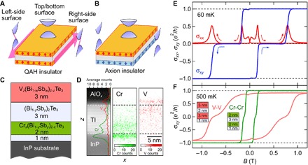
(A and B) Schematic depictions of the QAH and axion insulator states. Magnetization opens a gap in the top and bottom surface states. When the magnetizations (arrows) are parallel (A), 1D chiral edge channels are formed on the side surface. When the magnetizations are antiparallel (B), an energy gap opens also on the side surface. (C) Schematic structure of MBE-grown TI (BST) film doped with Cr and V used in the present study. The compositions: (x, y, z, w) = (0.24, 0.74, 0.15, 0.80). (D) Cross-sectional annular dark-field STEM (ADF-STEM) image (left) and net-count mappings of Cr (center) and V (right) obtained by an energy-dispersive x-ray spectroscopy (EDX) of the Cr-V–doped tricolor BST film, which are taken in the same area of the ADF-STEM image. x and z indicate the in-plane and out-of-plane directions of the film, respectively. Black bar indicates 5 nm in length. On the ADF-STEM image, averages along x of the net counts of Cr and V are indicated by green and red, respectively. (E) Magnetic field (B) dependence of Hall conductivity (σxy) and longitudinal conductivity (σxx) of the Cr-V–doped BST film at 60 mK. (F) Magnetic field (B) dependence of σxy at 500 mK in the Cr-Cr–doped [Cr0.24(Bi0.26Sb0.74)1.76Te3] (shown in green) and the V-V–doped [V0.15(Bi0.20Sb0.80)1.85Te3] (shown in red) bicolor TI heterostructures. Their growth profiles are depicted as insets with the respective thicknesses of the layers.
Experimental difficulties for observing the TME effect lies mostly in finding an appropriate materials system (21–23). Potent examples include Weyl semimetals with strong electron correlation, as exemplified theoretically in R2Ir2O7 (22) and AOs2O4 (R, rare earth element; A, alkali metal element) (23). However, the complexity of their electronic structure calls for further research. The lead candidate is the axion insulator state of a ferromagnetic 3D TI, where all the surface states are insulated while maintaining the nontrivial topology of the bulk state (3, 15–17). The axion insulator state has recently been demonstrated by engineering a TI heterostructure thin film of (Bi, Sb)2Te3 (BST) with magnetic ions (Cr) doped only in the vicinity of the top and bottom surfaces of the film (18). As a hallmark of the axion insulator, zero Hall conductivity (σxy) plateaus (ZHP) with simultaneous vanishing of longitudinal conductivity (σxx) were reported. Antiparallel magnetization alignment of the two magnetic layers, that is, magnetizations pointing upward and downward on the top and bottom surfaces, respectively (Fig. 1B), makes all the surface states insulating to realize the axion insulator. The antiparallel magnetization configuration arises from the difference in the coercive fields (Bc) of the two magnetic layers. In the previous work, the difference was probably imposed by a vertical asymmetry of the heterostructure, and hence, the magnetic field (B) for the axion insulator state was limited to a narrow range (for example, 0.12 T < B < 0.15 T at 40 mK).
Toward the observation of the TME effect, robust realization of the axion insulator state is strongly desirable in a wide range of external magnetic and electric fields (24, 25). Because the TME responses are expected to be proportional to the applied external fields, preparation of the axion insulator state in a wide range of magnetic and electric fields is advantageous to obtain large TME signals. In addition, a highly insulating state of the axion insulator is preferable to prevent screening of the electric field or relaxation of the induced polarization charge.
Here, we report the realization of a robust axion insulator state by tailoring a tricolor structure of magnetic TI thin film as shown in Fig. 1C. The tricolor structure was designed so that the two separated magnetic layers have different Bc. For the magnetic TI layers, we used Cr- (5–7, 9) and V-doped (8) BST, which were reported to exhibit the QAH effect. The values of Bc have been reported as 0.2 and 1 T for the Cr- and V-doped BST, respectively. Hence, if the magnetic coupling of the two layers is weak, this film structure is expected to exhibit a double-step magnetization reversal with antiparallel magnetization alignment between the two coercive fields. To ensure the magnetic decoupling of the two layers, we insert a nonmagnetic BST between the Cr- and V-doped layers. A total film thickness of 9 nm was chosen to weaken the hybridization between the top and bottom surface states (18, 26, 27). In this tricolor structure (Fig. 1C), the electrons on the bottom surface state interact with the Cr ions and those on top surface state interact with V ions.
RESULTS AND DISSCUSSION
The tricolor-structure film of Cr-doped BST (2 nm)/BST (3 nm)/V-doped BST (3 nm) (Cr-V–doped BST) was grown by molecular beam epitaxy (MBE) on the InP(111) substrate (Fig. 1C). To align the charge neutrality points for the top and bottom surface states, we modulated the Bi/Sb ratio at the Cr- and the V-doped layer (section S1). A 1-nm-thick BST was grown as a buffer layer between the substrate and the film for the improvement of the quality, providing enhancement in the observable temperature of the QAH effect (9). We also prepared Cr-Cr– and V-V–doped bicolor TI heterostructure films (insets of Fig. 1F) for comparison. Cross-sectional scanning transmission electron microscope (STEM) and EDX observations proved that Cr and V ions are distributed in the film as expected (Fig. 1D) (see also fig. S2 for more details). The films were fabricated into Hall bar and Corbino disk shapes for transport measurements (fig. S3).
Transport measurements on the Cr-V–doped BST film were conducted at 60 mK using a dilution refrigerator. Figure 1E shows the magnetic field (B) dependence of the Hall (σxy) and longitudinal (σxx) conductivities in a Hall bar device. Double-step transitions are observed in the B dependence of σxy. σxx has double peaks at the B of σxy transitions; otherwise, σxx is almost zero. Between the two transitions in σxy, the ZHP is observed in a range of 0.19 T < B < 0.72 T (see also fig. S4). Figure 1F shows the transport properties of the V-V–doped (3 nm) and Cr-Cr–doped (2 nm) BST heterostructure at 500 mK. The Bc of the Cr-Cr–doped and V-V–doped films are 0.2 and 0.8 T, respectively. The transition fields of the Cr-V–doped film (Fig. 1E) nearly correspond to the Bc of the Cr-Cr–doped (~0.2 T) and V-V–doped (~0.8 T) heterostructures. The correspondence unambiguously shows that the ZHP originates from the antiparallel magnetization alignment of the Cr- and V-doped layers. As shown in Fig. 1F, precursors of the ZHP are seen in the B dependence of σxy in the Cr-Cr–doped and V-V–doped films as well. However, the antiparallel magnetization in these films is probably induced by the unintentional difference in Bc between the upper and lower magnetically doped layers; therefore, the observed B range for the ZHP is very narrow compared to the Cr-V–doped film.
In Fig. 2A, we show the B dependence of σxy at various temperatures from 60 mK to 20 K. A kink structure is observed around the sign changes of σxy below 9 K, which develops into the ZHP with decreasing temperature. Below 300 mK, the ZHP is well established and the quantization of σxy to ±e2/h is seen at B = 0 T. In Fig. 2B, the values of Bc are plotted in the T-B plane for the Cr-V–doped and the Cr-Cr–doped films. The Bc is determined from the peak positions of dσxy/dB. The smaller and the larger Bc values are defined as Bc1 and Bc2, respectively. The area corresponding to the ZHP between the QAH states is highlighted as a white region. Compared to the Cr-Cr–doped film, the area of the ZHP is far extended in the T-B plane as designed. The Bc1 of the Cr-V–doped film roughly coincides with the Bc1,2 of the Cr-Cr–doped film. The area of the ZHP is extended not only along the magnetic field axis but also along the temperature axis in the Cr-V–doped film. Improved stability of the antiparallel magnetization configuration is probably responsible for the increase in the observable temperature of the ZHPs.
Fig. 2. Magnetic field and temperature dependence of zero σxy plateau.
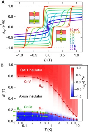
(A) Magnetic field dependence of σxy at representative temperatures in the Cr-V–doped tricolor TI film. (B) Color mapping of σxy for the Cr-V–doped TI tricolor film and plots of peaks for dσxy/dB, which correspond to coercive fields (defined as Bc1 for smaller and Bc2 for larger) of the Cr-V–doped tricolor film (shown in red) and the Cr-Cr–doped bicolor film (shown in green) in the T-B plane.
Next, we investigate the robustness of the ZHP states against the application of electric field using two-terminal transport measurements on the Corbino disk. In Fig. 3, we show current-voltage (I-V) characteristics of the Cr-V–doped tricolor film at 60 mK. The I-V curve displays an insulating behavior up to |V| ~ 10 mV. The application of |V| > 10 mV breaks down the insulating state, resulting in a steep increase in I. We compare the I-V characteristics of the Cr-V–doped film with those observed in the Cr-Cr–doped film. The breakdown voltage of the Cr-V–doped film is about five times larger than that of the Cr-Cr–doped film (|V| ~ 2 mV). Focusing on the I-V curves in the low-voltage regime (Fig. 3, insets), the two-terminal resistance reaches about 300 megohms in the Cr-V–doped film, which is about six times larger than that of the Cr-Cr–doped film (50 megohms). Thus, the stability of the axion insulator state against the electric field is also improved in the Cr-V–doped film compared to the Cr-Cr–doped film of the previous study (18). Although the relevant electric field direction for the TME effect is perpendicular to the film, the improved robustness against the in-plane electric field strongly suggests that the obtained axion insulator state is perhaps robust also to the perpendicular electric fields.
Fig. 3. I-V characteristics in tricolor and bicolor TI heterostructures.
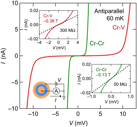
I-V curves under the antiparallel magnetization configuration of the Cr-V–doped tricolor BST (red) and the Cr-Cr–doped bicolor BST (green) heterostructures, taken in a Corbino disk device at T ~50 mK. For stabilization of the antiparallel magnetization configuration, the external magnetic field is fixed at the minimum of conductivity (for the Cr-V–doped BST, B = −0.38 T; for the Cr-Cr–doped BST, B = −0.13 T). Upper (lower) inset: Expanded scale of the I-V curve of the Cr-V–doped (Cr-Cr–doped) BST heterostructure.
The large two-terminal resistance of the axion insulator state leads to a gigantic magnetoresistance (MR) ratio. Figure 4A shows the B dependence of the two-terminal resistance (R2T) of the Hall bar device (width W = 300 μm and length L = 1 mm) at various temperatures. The R2T exhibits a butterfly shape when B is swept. The low resistance value of R2T = 28 kilohms under the parallel magnetization configuration jumps up by about 9000 times to 260 megohms under the antiparallel magnetization configuration. When the field scan is stopped at 0.38 T, the resistance value keeps increasing up to 2.8 gigohms with the elapsed time, perhaps because of the sample temperature, which was increased during the B scan (fig. S5), cooling down; this gives the MR ratio [= (R2TAP – R2TP)/R2TP, where AP and P denote the antiparallel and parallel magnetization configurations, respectively] exceeding 100,000 (or 10,000,000%). The gigantic MR is demonstrated within 2 T, being distinct from the extremely large MR (XMR) reported for other topological materials, such as WTe2 (28) and NbP (29), by applying a high magnetic field above 50 T. Even at 0.5 K, the MR ratio remains as high as 1800%, which is comparable to the XMR at B = 2 T. One other important and distinctive feature of the MR ratio in the present system is that the low resistance value R2TP is mainly dominated by the Hall resistance. Therefore, R2TP takes a value close to h/e2 and does not strongly depend on the dimensions of the Hall bar. On the other hand, the high resistance value R2TAP scales with the aspect ratio of the Hall bar as usual. As a result, the MR ratio associated with the QAH/axion insulator transition, which corresponds to the switching on/off of the chiral edge channels, becomes dependent on the Hall bar dimensions.
Fig. 4. Magnetic field and temperature dependence of two-terminal resistance in the Cr-V–doped tricolor TI.
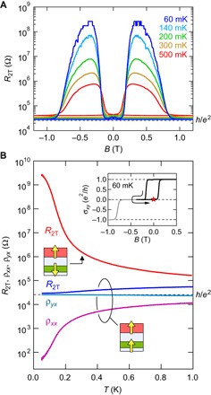
(A) Magnetic field (B) dependence of two-terminal resistance (R2T) between current terminals in the Hall bar of the Cr-V–doped BST film measured at various temperatures (T = 60, 140, 200, 300, and 500 mK). (B) Temperature (T) dependence of R2T in the parallel/antiparallel magnetization configurations under zero magnetic field. ρyx and ρxx measured by a four-terminal probe are also shown. Inset: minor loop hysteresis of σxy at T = 60 mK, reversing B at −0.38 T.
The axion insulator state with such a high resistance is maintained even when the field is swept back to B = 0 T. Figure 4B shows the temperature (T) dependence of R2T at B = 0 T under the antiparallel and parallel magnetization configurations (T dependence of ρxx and ρyx measured in the Hall bar are plotted together). The resistance under antiparallel magnetization is highly sensitive to T. By increasing T from 60 up to 400 mK, R2TAP decreases by three orders of magnitude. The high resistance values in Fig. 4A measured by scanning B probably suffered from the temperature increase during the B scan. This behavior contrasts to the R2T under the parallel configuration, which is mainly dominated by the Hall resistance and is only weakly dependent on T.
In conclusion, we have realized the robust axion insulator state by tailoring a tricolor structure of magnetic TI selectively doped with Cr and V. The observed wide ZHP width (0.19 T < B < 0.72 T at 60 mK) with a larger breakdown electric field is a crucial improvement in the testing of the TME effect. In addition, the on/off switching of the chiral edge current by magnetization reversal of the Cr-doped (soft ferromagnetic, Bc < 0.2 T) layer provides the gigantic MR ratio exceeding 10,000,000%. Because of the scale-invariant nature of the QAH state, the MR ratio in the present system depends on the sample geometry. This singularity in the MR effect of the tricolor structure of the magnetic TI would carve out a new strategy for electric circuit applications of chiral edge channels, in combination with the experimental technique of arbitrary magnetic domain writing/motion (30–32).
MATERIALS AND METHODS
Thin film growth
The TI heterostructures were grown by the MBE system. The substrate was a semi-insulating (>107 ohm·cm) InP(111)A and was annealed at 380°C in the chamber before growth. Bi, Sb, Te, and Cr were evaporated from standard Knudsen cells, and V was evaporated from the Knudsen cell customized for high-temperature use. For the growth of BST and Cr-doped BST, the growth rate was ~0.2 nm min−1 and the growth temperature was kept at 200°C. After the growth of the intermediate BST layer, the film was annealed in situ at 380°C for 30 min under exposure to Te. Subsequently, the V-doped BST layer was grown at a rate of 0.1 nm min−1 at 160°C. After the growth, a 3-nm-thick AlOx capping layer was immediately deposited ex situ by atomic layer deposition at room temperature.
Device fabrication
The films were patterned to the Hall bars and Corbino disks by conventional photolithography, Ar ion milling, and chemical wet etching processes. For ohmic contact electrodes, 3-nm-thick Ti and subsequent 27-nm-thick Au were deposited by electron beam evaporation. The dimensions of the Hall bars are 1000 × 300 μm, which has voltage probes separated by 300 μm. The inner and outer radii of the Corbino disk are 250 and 400 μm, respectively.
Transport measurement
Electrical transport measurements of the devices were performed in a dilution refrigerator or the Quantum Design physical property measurement system under the control of the magnetic field and temperature. Most of the measurements were performed by a standard lock-in technique with a fixed excitation current (1 to 10 nA) or voltage (0.1 to 5 mV) at low frequency (3 Hz). The I-V characteristic measurements were performed by a standard dc method.
Supplementary Material
Acknowledgments
We thank S. Shimizu for the experimental support. Funding: This research was supported by the Japan Society for the Promotion of Science (JSPS) through the Funding Program for World-Leading Innovative R&D on Science and Technology (FIRST Program) on “Quantum Science on Strong Correlation” initiated by the Council for Science and Technology Policy, JSPS/MEXT Grants-in-Aid for Scientific Research (nos. 24224009, 24226002, 15H05853, and 15H05867), and the Japan Science and Technology Agency Core Research for Evolutional Science and Technology (JST CREST) (no. JPMJCR16F1). M.M. is supported by JSPS through a research fellowship for young scientists (no. 17J03179). Author contributions: Y.T. and M.M. conceived and designed the research. M.M. grew the materials and performed the measurements and analysis with the help of M. Kawamura, R.Y., and K.S.T. M.M., M. Kawamura, A.T., M. Kawasaki, and Y.T. interpreted the results and wrote the manuscript with contributions from all the other authors. Competing interests: The authors declare that they have no competing interests. Data and materials availability: All data needed to evaluate the conclusions in the paper are present in the paper and/or the Supplementary Materials. Additional data related to this paper may be requested from the authors.
SUPPLEMENTARY MATERIALS
Supplementary material for this article is available at http://advances.sciencemag.org/cgi/content/full/3/10/eaao1669/DC1
section S1. Chemical potential tuning by Bi/Sb composition ratio
section S2. Elemental distributions in tricolor structure of magnetic TI film
section S3. Devices for transport measurements
section S4. Raw data of the four-terminal measurement
section S5. Time evolution of the two-terminal resistance
fig. S1. Chemical potential tuning on V-V–doped heterostructures.
fig. S2. Cross-sectional TEM and EDX analysis of tricolor magnetic TI heterostructure.
fig. S3. Images of devices used in the experiment.
fig. S4. B dependence of ρxx and ρyx of the Cr-V–doped tricolor TI.
fig. S5. Time dependence of the two-terminal resistance of the Cr-V–doped tricolor TI.
REFERENCES AND NOTES
- 1.Hasan M. Z., Kane C. L., Colloquium: Topological insulators. Rev. Mod. Phys. 82, 3045–3067 (2010). [Google Scholar]
- 2.Qi X.-L., Zhang S.-C., Topological insulators and superconductors. Rev. Mod. Phys. 83, 1057–1110 (2011). [Google Scholar]
- 3.Qi X.-L., Hughes T. L., Zhang S.-C., Topological field theory of time-reversal invariant insulators. Phys. Rev. B 78, 195424 (2008). [Google Scholar]
- 4.Yu R., Zhang W., Zhang H.-J., Zhang S.-C., Dai X., Fang Z., Quantized anomalous Hall effect in magnetic topological insulators. Science 329, 61–64 (2010). [DOI] [PubMed] [Google Scholar]
- 5.Chang C.-Z., Zhang J., Feng X., Zhang Z., Guo M., Li K., Ou Y., Wei P., Wang L.-L., Ji Z.-Q., Feng Y., Ji S., Chen X., Jia J., Dai X., Fang Z., Zhang S.-C., He K., Wang Y., Lu L., Ma X.-C., Xue Q.-K., Experimental observation of the quantum anomalous Hall effect in a magnetic topological insulator. Science 340, 167–170 (2013). [DOI] [PubMed] [Google Scholar]
- 6.Checkelsky J. G., Yoshimi R., Tsukazaki A., Takahashi K. S., Kozuka Y., Falson J., Kawasaki M., Tokura Y., Trajectory of the anomalous Hall effect towards the quantized state in a ferromagnetic topological insulator. Nat. Phys. 10, 731–736 (2014). [Google Scholar]
- 7.Kou X., Guo S.-T., Fan Y., Pan L., Lang M., Jiang Y., Shao Q., Nie T., Murata K., Tang J., Wang Y., He L., Lee T.-K., Lee W.-L., Wang K. L., Scale-invariant quantum anomalous Hall effect in magnetic topological insulators beyond the two-dimensional limit. Phys. Rev. Lett. 113, 137201 (2014). [DOI] [PubMed] [Google Scholar]
- 8.Chang C.-Z., Zhao W., Kim D. Y., Zhang H., Assaf B. A., Heimann D., Zhang S.-C., Liu C., Chan M. H. W., Moodera J. S., High-precision realization of robust quantum anomalous Hall state in a hard ferromagnetic topological insulator. Nat. Mater. 14, 473–477 (2015). [DOI] [PubMed] [Google Scholar]
- 9.Mogi M., Yoshimi R., Tsukazaki A., Yasuda K., Kozuka Y., Takahashi K. S., Kawasaki M., Tokura Y., Magnetic modulation doping in topological insulators toward higher-temperature quantum anomalous Hall effect. Appl. Phys. Lett. 107, 182401 (2015). [Google Scholar]
- 10.Maciejko J., Qi X.-L., Drew H. D., Zhang S.-C., Topological quantization in units of the fine structure constant. Phys. Rev. Lett. 105, 166803 (2010). [DOI] [PubMed] [Google Scholar]
- 11.Tse W.-K., MacDonald A. H., Giant magneto-optical Kerr effect and universal Faraday effect in thin-film topological insulators. Phys. Rev. Lett. 105, 057401 (2010). [DOI] [PubMed] [Google Scholar]
- 12.Okada K. N., Takahashi Y., Mogi M., Yoshimi R., Tsukazaki A., Takahashi K. S., Ogawa N., Kawasaki M., Tokura Y., Terahertz spectroscopy on Faraday and Kerr rotations in a quantum anomalous Hall state. Nat. Commun. 7, 12245 (2016). [DOI] [PMC free article] [PubMed] [Google Scholar]
- 13.Wu L., Salehi M., Koirala N., Moon J., Oh S., Armitage N. P., Quantized Faraday and Kerr rotation and axion electrodynamics of a 3D topological insulator. Science 354, 1124–1127 (2016). [DOI] [PubMed] [Google Scholar]
- 14.Dziom V., Shuvaev A., Pimenov A., Astakhov G. V., Ames C., Bendias K., Böttcher J., Tkachov G., Hankiewicz E. M., Brüne C., Buhmann H., Molenkamp L. W., Observation of the universal magnetoelectric effect in a 3D topological insulator. Nat. Commun. 8, 15197 (2017). [DOI] [PMC free article] [PubMed] [Google Scholar]
- 15.Essin A. M., Moore J. E., Vanderbilt D., Magnetoelectric polarizability and axion electrodynamics in crystalline insulators. Phys. Rev. Lett. 102, 146805 (2009). [DOI] [PubMed] [Google Scholar]
- 16.Morimoto T., Furusaki A., Nagaosa N., Topological magneto-electric effects in thin films of topological insulators. Phys. Rev. B 92, 085113 (2015). [Google Scholar]
- 17.Wang J., Lian B., Qi X.-L., Zhang S.-C., Quantized topological magnetoelectric effect of the zero-plateau quantum anomalous Hall state. Phys. Rev. B 92, 081107 (2015). [Google Scholar]
- 18.Mogi M., Kawamura M., Yoshimi R., Tsukazaki A., Kozuka Y., Shirakawa N., Takahashi K. S., Kawasaki M., Tokura Y., A magnetic heterostructure of topological insulators as a candidate for an axion insulator. Nat. Mater. 16, 516–521 (2017). [DOI] [PubMed] [Google Scholar]
- 19.Peccei R. D., Quinn H. R., CP conservation in the presence of pseudoparticles. Phys. Rev. Lett. 38, 1440–1443 (1977). [Google Scholar]
- 20.Wilczek F., Two applications of axion electrodynamics. Phys. Rev. Lett. 58, 1799–1802 (1987). [DOI] [PubMed] [Google Scholar]
- 21.Li R., Wang J., Qi X.-L., Zhang S.-C., Dynamical axion field in topological magnetic insulators. Nat. Phys. 6, 284–288 (2010). [Google Scholar]
- 22.Wan X., Turner A. M., Vishwanath A., Savrasov S. Y., Topological semimetal and Fermi-arc surface states in the electronic structure of pyrochlore iridates. Phys. Rev. B 83, 205101 (2011). [Google Scholar]
- 23.Wan X., Vishwanath A., Savrasov S. Y., Computational design of axion insulators based on 5d spinel compounds. Phys. Rev. Lett. 108, 146601 (2012). [DOI] [PubMed] [Google Scholar]
- 24.Fiebig M., Revival of the magnetoelectric effect. J. Phys. D Appl. Phys. 38, R123 (2005). [Google Scholar]
- 25.Rivera J.-P., A short review of the magnetoelectric effect and related experimental techniques on single phase (multi-) ferroics. Eur. Phys. J. B. 71, 299 (2009). [Google Scholar]
- 26.Liu C.-X., Zhang H., Yan B., Qi X.-L., Frauenheim T., Dai X., Fang Z., Zhang S.-C., Oscillatory crossover from two dimensional to three dimensional topological insulators. Phys. Rev. B 81, 041307 (2010). [Google Scholar]
- 27.Zhang Y., He K., Chang C.-Z., Song C.-L., Wang L.-L., Chen X., Jia J.-F., Fang Z., Dai X., Shan W.-Y., Shen S.-Q., Niu Q., Qi X.-L., Zhang S.-C., Ma X.-C., Xue Q.-K., Crossover of the three-dimensional topological insulator Bi2Se3 to the two-dimensional limit. Nat. Phys. 6, 584–588 (2010). [Google Scholar]
- 28.Ali M. N., Xiong J., Flynn S., Tao J., Gibson Q. D., Schoop L. M., Liang T., Haldolaarachchige N., Hirschberger M., Ong N. P., Cava R. J., Large, non-saturating magnetoresistance in WTe2. Nature 514, 205–208 (2014). [DOI] [PubMed] [Google Scholar]
- 29.Shekhar C., Nayak A. K., Sun Y., Schmidt M., Nicklas M., Leermakers I., Zeitler U., Skourski Y., Wosnitza J., Liu Z., Chen Y., Schnelle W., Borrmann H., Grin Y., Felser C., Yan B., Extremely large magnetoresistance and ultrahigh mobility in the topological Weyl semimetal candidate NbP. Nat. Phys. 11, 645–649 (2015). [Google Scholar]
- 30.Yeats A. L., Mintun P. J., Pan Y., Richardella A., Buckley B. B., Samarth N., Awschalom D. D., Local optical control of ferromagnetism and chemical potential in a topological insulator. Proc. Natl. Acad. Sci. U.S.A. https://arxiv.org/abs/1704.00831 (2017). [DOI] [PMC free article] [PubMed] [Google Scholar]
- 31.Fan Y., Upadhyaya P., Kou X., Lang M., Takei S., Wang Z., Tang J., He L., Chang L.-T., Montazeri M., Yu G., Jiang W., Nie T., Schwartz R. N., Tserkovnyak Y., Wang K. L., Magnetization switching through giant spin–orbit torque in a magnetically doped topological insulator heterostructure. Nat. Mater. 13, 699–704 (2014). [DOI] [PubMed] [Google Scholar]
- 32.Yasuda K., Tsukazaki A., Yoshimi R., Kondou K., Takahashi K. S., Otani Y., Kawasaki M., Tokura Y., Current-nonlinear Hall effect and spin-orbit torque magnetization switching in a magnetic topological insulator. https://arxiv.org/abs/1612.06862 (2016). [DOI] [PubMed] [Google Scholar]
Associated Data
This section collects any data citations, data availability statements, or supplementary materials included in this article.
Supplementary Materials
Supplementary material for this article is available at http://advances.sciencemag.org/cgi/content/full/3/10/eaao1669/DC1
section S1. Chemical potential tuning by Bi/Sb composition ratio
section S2. Elemental distributions in tricolor structure of magnetic TI film
section S3. Devices for transport measurements
section S4. Raw data of the four-terminal measurement
section S5. Time evolution of the two-terminal resistance
fig. S1. Chemical potential tuning on V-V–doped heterostructures.
fig. S2. Cross-sectional TEM and EDX analysis of tricolor magnetic TI heterostructure.
fig. S3. Images of devices used in the experiment.
fig. S4. B dependence of ρxx and ρyx of the Cr-V–doped tricolor TI.
fig. S5. Time dependence of the two-terminal resistance of the Cr-V–doped tricolor TI.