Abstract
Thin films of PbZr0.52Ti0.48O3 (PZT) with largely detached columnar grains, deposited by pulsed laser deposition (PLD) on amorphous glass substrates covered with Ca2Nb3O10 nanosheets as growth template and using LaNiO3 electrode layers, are shown to exhibit very high unipolar piezoelectric strain and ultra-low strain hysteresis. The observed increase of the piezoelectric coefficient with increasing film thickness is attributed to the reduction of clamping, because of the increasingly less dense columnar microstructure (more separation between the grains) with across the film thickness. A very large piezoelectric coefficient (490 pm/V) and a high piezoelectric strain (~0.9%) are obtained in 4-µm-thick film under an applied electric field of 200 kV/cm, which is several times larger than in usual PZT ceramics. Further very low strain hysteresis (H≈2–4%) is observed in 4 to 5 µm thick films. These belong to the best values demonstrated so far in piezoelectric films. Fatigue testing shows that the piezoelectric properties are stable up to 1010 cycles. The growth of high quality PZT films with very large strain and piezoelectric coefficients, very low hysteresis and with long-term stability on a technologically important substrate as glass is of great significance for the development of practical piezo driven microelectromechanical actuator systems.
Introduction
Microelectromechanical systems (MEMS) actuators driven by piezoelectric materials such as lead zirconate titanate with the morphotropic phase boundary, PbZr0.52Ti0.48O3 (PZT), composition, have received wide attention because they can potentially outperform other MEMS actuators, because of the remarkably high ferroelectric polarization and piezoelectric coefficients of PZT1,2. For most MEMS device applications, such as vibration energy harvesters, micropumps, microcantilever-based mass sensors and micromachined ultrasonic transducers for medical and sonar applications, the (effective) transverse piezoelectric coefficient (e 31f or d 31f) of the film is the most important factor to be considered. For specific applications however, such as nanometer-position control systems based on piezoelectric actuators for the control of optical cavities or short wavelength mirrors3, a large (effective) longitudinal piezoelectric coefficient (d 33f) is required to obtain a large piezoelectric deformation in the PZT thin film capacitors.
The high piezoelectric response in ceramic PZT is due not only to the deformation of the crystal unit cells (intrinsic effect) but also due to the motion of domain walls, polarization switching and the motion of phase boundaries (extrinsic effect)4. Domain wall motion and domain switching contributes in a significant way to the increase of piezoelectricity, but it is only useful these processes are reversible. However, polarization switching is in an unipolar driven actuator device an irreversible process and the associated significant piezoelectric enhancement is useless5. There is evidence that nonlinear behaviour is related to the domain switching in the piezoelectric materials6,7. Under an applied electric field the spontaneous polarization of domains may be reoriented, which is commonly called ferroelectric of ferroelastic domain switching. The nonlinearity (or strain hysteresis) that appears in piezoelectric material is also ascribed to the domain switching related irreversible polarization and piezoelectric strain.
For actuators used in practice, the electric field is applied tom a component along its poling axis (3-direction). The resulting electric field-induced piezoelectric strain (S 3) can be described as:
| 1 |
where, s33σ3 represents the mechanical elastic strain, S′3 and d * 33 E 3 are the domain switching-related irreversible strain and the contribution of the reversible inverse piezoelectric effect, respectively. A large-signal electric field leads to ferroelastic domain switching in the piezoelectric materials. Due to the change of strain, the material parameters in Eq. (1) are no longer constant, but depend on the history of the applied electric field. As a result, the actual response of piezoelectric materials will display significant hysteresis and nonlinearity.
Piezoelectric materials with (strongly) enhanced longitudinal piezoelectric displacement (or piezoelectric strain) were presented. However most studies reporting on large strain are limited to bulk ceramics of piezoelectric materials due to the difficulty of growing thin films with similar piezoelectric response as in ceramic form. Lead-based piezoelectric ceramics, such as the soft PZT (PZT-5H) ceramics have a maximum strain (S max) of 0.175%, corresponding to a normalized piezoelectric coefficient of 730 pm/V and a relative strain hysteresis ( with the strain on the rising (falling) branch of the hysteresis loop at half the maximum applied field E max. At maximum field the strain is S max) of 12% for E max = 24 kV/cm. A lower strain (S = 0.105%, equivalent to = 250 pm/V) and a lower H value of 5% were obtained in the hard PZT (PZT-8) ceramics, for E max = 42 kV/cm8.
Many studies have been performed to find lead-free piezoelectric ceramics as an alternative for the PZT materials. Yao et al. reported that the large piezoelectric coefficient (d 33) of 280 pm/V, and a strain of 0.28% (under an E max of 56 kV/cm), and a high normalized coefficient of 833 pm/V (at low E max of 18 kV/cm) in (K,Na,Li)(Nb,Ta,Sb)O3 ceramics9. Similar high values (S = 0.23% at E max = 50 kV/cm) were obtained in the (lead containing) Pb(Yb0.5Nb0.5)O3-PbHfO3-PbTiO3 composition10. Recently very high strains have been observed in (Fe-Sb)-codoped (Bi0.5Na0.5)1−xBaxTi0.98O3 (BNT–BT) ceramics (S = 0.57%, = 713 pm/V at E max = 80 kV/cm)11 and in NaNbO3-doped Bi0.5Na0.5TiO3–Bi0.5K0.5TiO3 (BNT–BKT) ceramics (S = 0.445%, = 810 pm/V at E max = 55 kV/cm)12. However, the strain hysteresis (H) values of these ceramics were very high, such as H≈70% for the (Fe-Sb)-codoped BNT–BT system11 and H≈60% for the NaNbO3-doped BNT–BKT system12. These results indicate that high values of strain in piezoelectric ceramics are often accompanied by large strain hysteresis, which limits the useful application in piezoelectric actuators.
Piezo-driven actuators have recently been used in adaptive optics, deformable mirrors, camera modules, as well as in high-resolution positioning stages with the range of motion from nano- to micro-meters13–15. For the integration of piezoelectric materials in such systems, in many cases the piezoelectric materials should be prepared in thin-film form on glass substrates. Although the lead-free ceramics have high piezoelectric responses, there is great difficulty in growing these materials in thin film form with similar piezoelectric response as in ceramic form. Therefore piezoelectric MEMS devices based on PZT are nowadays still widely used in both research and development and in commercial products. In a previous paper, we demonstrated that the piezoelectric coefficient (d 33f) of PZT films deposited on Pt/Ti/SiO2/Si by PLD, can be enhanced strongly by using vertically oriented columnar growth16. A high d 33f value of 408 pm/V was found in 4 µm thick PZT films, which corresponds fairly well with the theoretical result of Cao et al. (525 pm/V for x Ti = 0.48)17. This value is much larger than the theoretical value for PZT single-crystal and single-domain from Haun et al. (327 pm/V)18 and also larger than typical experimental values found for bulk PZT ceramics (d 33 = 223 pm/V)19. We also investigated the effect of microstructure and orientation on the piezoelectric properties of such PZT films. Further we demonstrated a high d 33f of 356 pm/V in columnar grown (001)-oriented 2-µm-thick PZT films on amorphous glass substrates20.
In this work, we describe the fabrication of (001)-oriented PbZr0.52Ti0.48O3 (PZT) thin films on Ca2Nb3O10 nanosheets (CNOns) coated amorphous glass substrates, using conductive oxide LaNiO3 (LNO) layers as top and bottom electrodes. We achieve very high piezoelectric strain and low strain hysteresis as a result of the vertically oriented columnar growth technique. We investigate in detail the influence of film thickness on the microstructure and piezoelectric response. Extremely large strain response of 0.9% was obtained in 4-µm-thick PZT films with pm/V, together with a low strain hysteresis of 4% for E max = 200 kV/cm. A very large value of 690 pm/V was obtained in this film for E max = 55 kV/cm (or an applied voltage of 22 V), resulting in a displacement of 15 nm. In addition, to evaluate the long-term reliability, fatigue measurements of unipolar strain/displacement were also performed.
Results and Discussion
By varying the PZT film thickness changes of the microstructure over the thickness were obtained in films grown on LaNiO3 (LNO) buffered CNOns/glass substrates. We observe notable effects of these differences in the ferroelectric and piezoelectric properties of these PZT film capacitors that we relate to changes in substrate clamping.
In order to investigate the effect of the film thickness on the structures and electrical properties, several PZT films with thicknesses ranging from 1 to 5 µm were prepared using PLD. Fig. S2a shows the XRD patterns of PZT films with different thicknesses deposited on LNO buffered CNOns/glass substrates at a laser repetition frequency of 50 Hz. Clearly all the films have crystallized in a pure perovskite phase with a (001)-preferred orientation and no evidence of secondary phase formation, such as the pyrochlore phase, was detected. As the film thickness increases, the peak intensity of the (001) plane increases as well whereas the peak intensity of the (110) plane decreases, indicating that (110) growth mainly occurs at the bottom of the film and is suppressed when the film growth continues. The crystalline quality was further determined from the rocking curve widths of the PZT(002) reflections as shown in Fig. S2b. With increasing film thickness the FWHM value of the rocking curve increases, indicating that the average grain tilt increases, but maintaining the (001) growth orientation in the grains.
AFM and SEM micrographs of the surfaces and cross-sections of the PZT films deposited on CNOns/glass are shown in Fig. S3 and Fig. 1, respectively. From the AFM surface micrographs it is seen that the grain diameter and the distances between the grains become larger with film thickness. AFM line scans spectra in Fig. S4 show an increase in the surface height fluctuations of the films with increasing thickness from about 70 nm for the 1 µm film to 190 nm for the 5 µm film. The root-mean square surface roughness (R rms) increases from 23 to 56 nm. The SEM cross-sectional images show that the columnar grains extend through the complete thickness of the PZT films. The average width of the grains at the top of the layers increases from about 120 to 268 nm as the film thickness changes from 1 to 5 µm (see Table 1). Previously it was also shown that for the used deposition conditions with increasing thickness the columnar grains become increasingly detached from each other, reducing the effect of film clamping by the substrate16.
Figure 1.
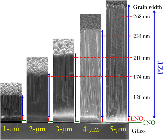
Cross-sectional SEM images of PZT films with various thicknesses deposited on LNO/CNOns/glass.
Table 1.
Properties of PZT films as a function of film thickness.
| Film thickness (µm) | Rocking curve FWHM of ω-scan of PZT(002) (°) | R rms (nm) | Column diameter d col (nm) a | P r (µC/cm2) | E c (kV/cm) | d 33f b (pm/V) | c (pm/V) |
|---|---|---|---|---|---|---|---|
| 1.0 | 0.55 | 23.2 | 120 | 22.0 | 37.4 | 227 | 265 |
| 2.0 | 0.67 | 32.1 | 174 | 28.1 | 35.0 | 356 | 390 |
| 3.0 | 0.96 | 39.3 | 210 | 30.0 | 30.3 | 460 | 458 |
| 4.0 | 1.16 | 42.7 | 234 | 30.0 | 30.2 | 490 | 450 |
| 5.0 | 1.34 | 56.0 | 268 | 27.4 | 25.7 | 454 | 430 |
aat the top of the layer; bdetermined at E = 0 kV/cm from d 33f −E hysteresis loops up to 200 kV/cm at 1 kHz scan frequency; cdetermined from unipolar S-E loops up to 200 kV/cm at 10 Hz scan frequency.
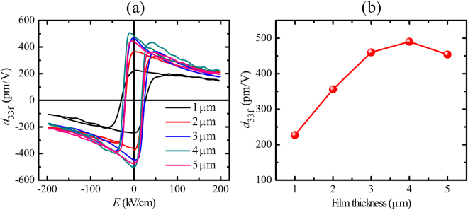
Ferroelectric and piezoelectric properties of the PZT films have been investigated as a function of thickness. Fig. S5a shows the P-E hysteresis loops. The remanent polarization (P r) value increases with film thickness and reaches a maximum value of about 30.0 µC/cm2 at a thickness of 3 µm, while the coercive field (E c) decreases continuously with increasing film thickness (Fig. S5b). The electric-field dependence of the small-signal effective piezoelectric coefficient (d 33f–E) for the different film thicknesses is shown in Fig. 2a. The zero field d 33f values increase from 227 to 490 pm/V as the film thickness increases from 1 to 4 µm, and then slightly decreases for the 5 µm film (Fig. 2b). The Fig. 2a further indicates that the d 33f value strongly decreases with increasing electric field. In this case the polarization vectors are largely aligned parallel to the applied field and only the intrinsic piezoelectric effect contributes to d 33f. Therefore, the d 33f values peak in the low electric field region, where extrinsic contributions to the piezoelectric effect are largest and gradually decreases at higher electric fields where wall motion does not contribute to the piezoelectric effect any more.
Figure 2.
(a) Small-signal d 33f–E loops and (b) thickness dependence of d 33f, of PZT films with varying thicknesses deposited on LNO/CNOns/glass.
The effect of film thickness on the ferroelectric and piezoelectric properties can be explained by the contribution of domain structure changes related to the change in substrate clamping. Ferroelectric and piezoelectric properties are generally considered to originate from both intrinsic and extrinsic contributions as was demonstrated by Kim et al.21 and Xu et al.22. The intrinsic contribution originates from the response of a single polarization domain, whereas extrinsic contributions originates from the motion of the domain walls and phase boundaries23. The bottom of the films are tensile clamped due to thermal expansion coefficient difference between the film (TEC ≈ 5 ppm/K) and the substrate (TEC ≈ 0 ppm/K), causing some polarization rotation towards the film plane, but at larger thickness the grains are detached and the grains in the film are increasingly strain relaxed and the polarization rotates more in the out of plane direction. Therefore, an enhanced P r value is obtained for less tensile stress, which is here the case with increasing film thickness24. Similarly the polarization domains in the films are less clamped due to the reduction of substrate constraints, so that reverse domain nucleation becomes easier and then the P r value increases while the coercive field decreases with increasing film thickness. Further the increased effective d 33f coefficient with increasing film thickness is caused by a reduction of the clamping and the associated enhancement of the domain wall motion and switching in the increasingly freestanding grains25. In the previous study16, we have also discussed on the effect of film thickness on the microstructure and properties of PZT films grown on Pt/Ti/SiO2/Si (Pt/Si) substrates, in which the grains in the films can be considered to be polydomain single crystals. With increasing thickness the grains become less connected with neighbouring grains (as can be seen in Fig. S4 where the surface height fluctuations of the films increase with increasing thickness) and the effect of clamping on domain wall motion, polarization rotation and crystal unit cell deformation is reduced. Table 1 indicates that the values of P r and piezoelectric coefficient (d 33f or ) are reasonably saturated at the film thickness of 3–4 µm. However, this saturated thickness value is not constant and depends on the many factors such as the type of ferroelectric films, electrodes and substrates. Kim et al. indicated that the epitaxial PZT films grown on SrTiO3 and SrTiO3/Si substrates have the saturated thickness of about 2 µm25 and similar to the case of polycrystalline PZT films on Pt/Si26, while the maximum values of ferroelectric and piezoelectric properties were obtained at the film thickness of about 1 µm in the epitaxial PZT films grown on YSZ/Si substrates24. However, the maximum value of P r was obtained at quite thinner film (330 nm) in the BiFeO3 thin films deposited on SrRuO3 buffered Pt/Si substrates27.
A high value of the effective piezoelectric coefficient d 33f is the important parameter for e.g., sensors or ultrasonic devices; while the normalized strain piezoelectric coefficient () is the key parameter that matters in actuator systems. The normalized strain value is calculated as:
| 2 |
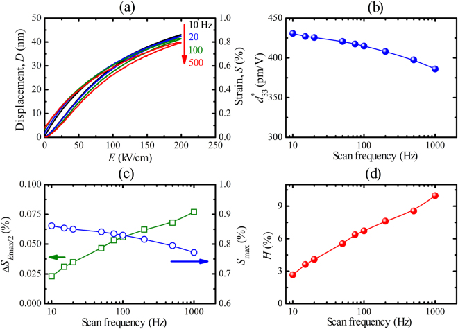
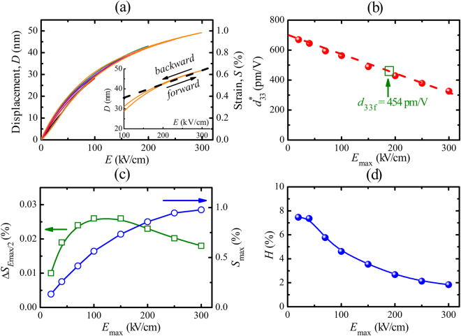
In order to evaluate the piezoelectric strain and strain hysteresis responses for practical applications in actuators, the dependence on the measurement (scan) frequency and the maximum applied electric field is investigated. In this study, the unipolar strain and strain hysteresis behaviour of a 5-µm-thick PZT film was evaluated as a function of scan frequency from 10 to 1000 Hz (at an electric field of 200 kV/cm; see Fig. 3a) and as a function of applied electric field up to 300 kV/cm at 10 Hz (Fig. 4a).
Figure 3.
(a) Unipolar piezoelectric displacement (D–E) and strain versus E-field (S–E) loops as a function of scan frequency for 5 µm PZT film. Scan frequency dependence of (b) normalized at E max, (c) fraction of the unipolar strain at E max/2 (ΔS Emax/2) and strain at E max (S max) and (d) strain hysteresis (H), with E max = 200 kV/cm.
Figure 4.
(a) Unipolar piezoelectric displacement (D–E) and strain versus E-field (S–E) loops for 5-µm-thick PZT film. E–field dependence of (b) normalized at E max, (c) fraction of the unipolar strain at E max/2 (ΔS Emax/2) and strain at E max (S max), and (d) strain hysteresis (H).
Figure 3a–d show the unipolar piezoelectric displacement (D–E), the unipolar strain (S–E, S = 100% × D/t, where t is the PZT film thickness) curves, the maximum strain (S(E max) or S max), the normalized values and the relative strain hysteresis (H), that is related to the piezoelectric loss, of the 5 µm film as a function of scan frequency. Both S max (Fig. 3c) and (Fig. 3b) values slightly decline when the frequency increases, whereas H values (Fig. 3d) significantly increase with increasing frequency. S max and reach maximum values (0.86% and 431 pm/V) and low H value (2.7%) is obtained at the scan frequency of 10 Hz. It is known that the domain wall motion and domain wall switching are a time dependent process28–30, thus one can expect that with increasing driving frequencies the H value is increased, and S max and values are slightly decreased.
The piezoelectric strain (S–E) curves and normalized values of the 5-µm-thick PZT film as a function of applied electric field (scan frequency: 10 Hz) are presented in Fig. 4a and b. The maximum strain values gradually increase with increasing applied electric field reaching a maximum value of about 1% at E max = 300 kV/cm (or V max = 150 V), as shown in Fig. 4c. Simultaneously H drops continuously with increasing E max (Fig. 4d). This huge S max value (~1%) with ultra-low strain hysteresis (H≈1.8%) belongs to the best values for piezoelectric films. The S max value used in this study is much higher than that of for example PZT4 bulk ceramics (S = 0.35% at E max = 20 kV/cm)31. The inset of Fig. 4a shows that the forward and backward displacements are nearly overlapping in the 150–300 kV/cm range which is of great advantage for real application in actuators.
The curve is linear up to about E max = 15 kV/cm and above this value the slope decreases and the curve tends to saturate (Fig. 4c). Therefore a large value of about 670 pm/V is obtained at a low applied electric field of 20 kV/cm, as indicated in Fig. 4b, but decreases approximately linearly with increasing E max. It is also interesting to note that the value at low applied electric field (<150 kV/cm) is much larger than the small-signal piezoelectric coefficient value (at zero field). In both measurement methods (small-signal measurement for d 33f and large-signal measurement for ) one expects that the intrinsic piezoelectric effect is approximately the same for both the small-signal d 33f–E and the large-signal unipolar strain S–E. On the other hand, the extrinsic contribution is sensitive to the mode of external excitation. For the d 33f–E measurement, a low external ac voltage of 400 mV was applied, a value well below the coercive field, thus there is negligible contribution from domain wall depinning and subsequent motion. There is still an extrinsic contribution from domain wall oscillation. The piezoelectric unipolar strain was measured with a large ac amplitude well-above the coercive field that makes domain wall depinning possible and significant domain wall motion. Therefore one may expect that a higher extrinsic contribution from domain wall motion to the strain is the origin of the larger value as compared to d 33f at an electric field below 150 kV/cm. As discussed above at higher fields there is increasingly less domain wall motion, since all polarization becomes aligned leading to the decrease in and d 33f(E).
The effect of electric-field induced domain wall motion and switching can also be seen in the strain hysteresis (Fig. 4d). The strain hysteresis (H) is high at the low electric fields, reflecting the large contribution from the pinning of domain wall motion, but with increasing field this effect decreases, since the contribution of domain wall motion to the total strain decreases.
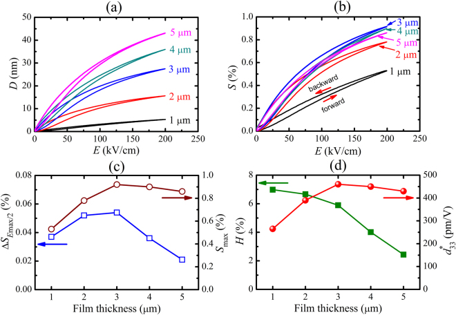
In order to investigate the effect of film thickness on the hysteresis in the piezoelectric displacement and strain, the unipolar piezoelectric displacements of PZT films in the range of 1–5 µm thick were measured with a maximum applied electric field of 200 kV/cm and at 10 Hz scan frequency. Slim piezoelectric displacement (D–E) curves are observed for all films (Fig. 5a). The large enhancement of the maximum displacement from 5.3 nm for the 1-µm-thick film to 43.0 nm for 5-µm-thick film implies that the displacement increases more than linear with the thickness. Of course the required driving voltage also increases from 20 to 100 V. Figure 5b shows the unipolar strain curves measured up to 200 kV/cm. Note that the largest strains are obtained for the films with thickness in the range 3–4 µm. The maximum strain and values of PZT films are presented in Fig. 5c–d. It is seen that the S max and values increase with increasing film thickness and reach the maximum values of 0.92% and 460 pm/V for the film thickness of 3 µm. On further increasing thickness S max and values decrease.
Figure 5.
(a) Unipolar piezoelectric displacement versus E–field (D–E) and (b) unipolar strain versus field (S–E) loops of PZT films with different thicknesses. Thickness dependence of (c) S max and fraction of the unipolar strain at E max/2 (ΔS Emax/2), and (d) large-field and relative strain hysteresis (H). The measurements were done at a scan frequency of 10 Hz.
Figure 5d also shows the relative strain hysteresis (H) of the films with different thicknesses. H decreases continuously with increasing film thickness reaching a very low H value of 2.4% in the 5-µm-thick film (at E max = 200 kV/cm). The reduced H is partly due to the reduced opening ΔS (Fig. 5c) of the strain loops for thicknesses larger than 2–3 µm, which suggests reduced domain wall pinning, and partly due to the increasing value of S max with increasing thickness.
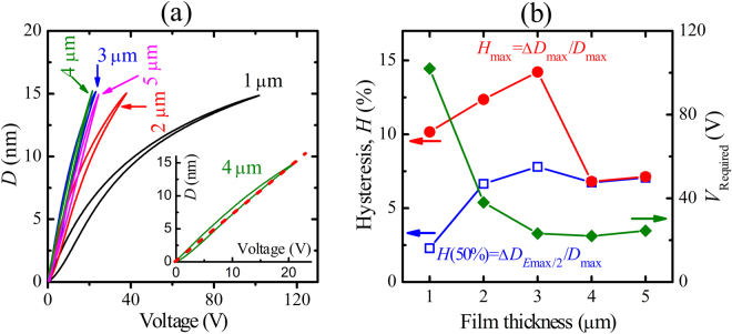
The above results demonstrate that for the same applied field, an enhanced piezoelectric displacement and low strain hysteresis are obtained in the thicker PZT films. However for some specific applications a specific maximum piezoelectric displacement is required. Figure 6a shows the unipolar piezoelectric displacement curves of PZT films with the same maximum displacement of 15 nm, by adjusting the maximum applied voltage (or electric field). The required voltages are about 102, 38, 23.2, 22 and 24.5 V for the films with the thickness of 1, 2, 3, 4 and 5 µm, respectively ( values from 0 V up to this voltage are respectively 146, 396, 653, 690 and 620 pm/V), as shown in Fig. 6b. The lowest applied voltage is needed for the 3–4 µm thick films. This means that low voltage driven actuators can be fabricated that achieve large piezoelectric displacements. This may open up good prospects for the application of such piezo-electric films. The films show the low train hysteresis of about 7–7.5%, except for the 1-µm-thick film with H value of 2.3% due to the high applied voltage in the measurement.
Figure 6.
(a) Unipolar piezoelectric displacement (D–V) loops, and (b) Strain hysteresis defined at ΔD Emax/2 and ΔD max and required applied voltage (V required) for the about 15-nm displacement of film capacitors. The measurements were done at a scan frequency of 10 Hz.
Moreover, Fig. 6a also indicates that the piezoelectric strain value as high as 0.375% under low electric field of 55 kV/cm is obtained in the 4-µm-thick PZT film. This value is comparable with the superior strain in lead-free materials, such as NaNbO3-doped Bi0.5Na0.5TiO3–Bi0.5K0.5TiO3 (0.445%)12, 0.965K0.45Na0.55Nb0.98Sb0.02O3–0.035Bi0.5Na0.5Zr0.85Hf0.15O3 (0.325%)32, but in the bulk ceramic form. Further the piezoelectric coefficient of 690 pm/V in the 4-µm-thick PZT film is also equivalent to that in the lead-free (Bi0.5Na0.5)TiO3–BaTiO3 (BNT-based) and (Ba,Ca)(Zr,Ti)O3 ceramics33. This also confirms the applicability of our PZT films for piezoelectric MEMS actuator devices.
In addition to the large piezoelectric coefficient, high piezoelectric strain and low strain hysteresis, long-term stability of these properties under working conditions is essential for the application of such films in practical devices. Figure 7 shows the piezoelectric displacement (and ) of the 4-µm-thick PZT film up to 1010 bipolar cycles (100 kV/cm at 100 kHz). Hardly any fatigue is present this piezoelectric film, suggesting that these films have excellent potential for demanding high cycle applications such as in MEMS actuators.
Figure 7.
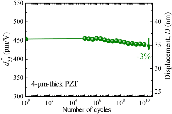
Piezoelectric displacement and large-signal value of 4-µm-thick PZT film as a function of working cycles, defined from the unipolar D-E loops measured at 200 kV/cm and 10 Hz. The fatigue testing was performed by applying a bipolar triangular field of 100 kV/cm and at 100 kHz.
Conclusions
We have shown that the microstructure of PZT films changes over the thickness of thick films. With increasing thickness the columnar grains become more separated and consequently less clamped by each other and the substrate. This causes a change in the piezoelectric and ferroelectric properties. The piezoelectric coefficients are significantly higher for the thicker films. A large d 33f of 490 pm/V, and a high strain of 0.9% (= 450 pm/V) with a low strain hysteresis of 4% were observed in 4-µm-thick PZT film measured at 200 kV/cm. For a displacement of 15 nm the applied voltage is only 22 V (corresponding to E = 55 kV/cm), which amounts to a very large value of 690 pm/V over the 0–55 kV/cm voltage range. The joint effects of vertically (001)-oriented columnar growth and thickness contribution (the film-electrode interfacial layer and substrate constrains effects are reduced with the thicker film) were identified to be the origin of the superior piezoelectric performance in this film. The combination of large piezoelectric strain and low strain hysteresis makes these films very suitable for piezoelectric actuator applications that require large displacements. Moreover, excellent fatigue resistance was observed in the films up to 1010 bipolar cycles. This finding demonstrates that these materials have excellent potential for demanding high cycle applications such as MEMS actuators.
Methods
Pb(Zr0.52Ti0.48)O3 (PZT) films were grown on 200-nm-thick LaNiO3 (LNO) electrodes which in turn were deposited on CNOns coated glass substrates using pulsed laser deposition (PLD) with a KrF excimer laser source (Lambda Physik, 248 nm wavelength). In this study, Ca2Nb3O10 (CNOns) nanosheets were fabricated on glass substrates by exfoliation of layered protonated calcium niobate, HCa2Nb3O10•1.5H2O, followed by the Langmuir-Blodgett (LB) deposition method. The details of the flux synthesized, layered precursor KCa2Nb3O10 and its protonation process can be found in previous papers34,35. An AFM image of a monolayer CNO nanosheet on glass is shown in Fig. S1. The deposition conditions for the PZT films were: laser repetition rate 50 Hz, energy density 2.5 J/cm2, oxygen pressure 0.1 mbar and a substrate temperature of 600 °C. For the LNO electrodes the deposition conditions were 4 Hz, 2.5 J/cm2, 0.1 mbar O2 and 600 °C. All layers were deposited successively without breaking the vacuum. After deposition the films were cooled down to room temperature in a 1 bar oxygen atmosphere at a ramp rate of 8 oC/min.
The crystal structure of the thin films was analyzed by X-ray diffraction θ–2θ scans (XRD, Philips X’Pert X-ray diffractometer). The microstructure was investigated using atomic force microscopy (AFM: Bruker Dimension Icon). For electrical measurements, 300 × 300 µm2 capacitors were patterned with a standard photolithography process and structured by argon-beam etching of the top-electrodes and wet-etching (HF-HCl solution) of the PZT films. The ferroelectric hysteresis (P-E) loops were measured with the ferroelectric mode of the aixACCT TF-2000 Analyzer, using a triangular ac-electric field of ±200 kV/cm at 1 kHz scanning frequency. The zero-field longitudinal piezoelectric coefficient (d 33f) of the piezoelectric thin-film capacitors was defined from the hysteresis loop of the piezoelectric coefficient (d 33f–E), measured by a double-beam laser interferometer (aixDBLI) method with a dc driving field between ±200 kV/cm on which an ac voltage of 400 mV (corresponding to 4 kV/cm for a 1-µm-thick film, down to 0.8 kV/cm for a 5-µm-thick film) and 1 kHz was superimposed (small-signal measurement). For the piezoelectric strain (S–E) measurement, an unipolar triangular-shaped ac electric field was applied to the film with 200 or 300 kV/cm amplitude at 10 Hz and the piezoelectric displacement was traced at the same time (large-signal measurement). The piezoelectric cycling fatigue measurements were performed with a bipolar switching pulse of 100 kV/cm pulse height at 100 kHz repetition frequency.
Electronic supplementary material
Acknowledgements
This research was financial supported by the project number M62.3.10404 in the framework of the Research Program of the Materials innovation institute (M2i) (www.m2i.nl) and by the NanoNextNL - a micro and nanotechnology consortium of the Government of the Netherlands and 130 partners. The authors thank Dr. Huiyu Yuan and Prof. Johan E. ten Elshof for the nanosheet deposition, and Mr. Mark Smithers for performing the HRSEM experiment.
Author Contributions
M.D.N. and G.R. conceived and designed the experiments. M.D.N. deposited the piezoelectric films, designed and fabricated the device structures, performed and analysed the ferroelectric and piezoelectric characterizations. M.D.N., E.P.H., and G.R. wrote the paper. All authors discussed the results, commented on the manuscript and gave their approval to the final version of the manuscript.
Competing Interests
The authors declare that they have no competing interests.
Footnotes
Electronic supplementary material
Supplementary information accompanies this paper at 10.1038/s41598-017-13425-w.
Publisher's note: Springer Nature remains neutral with regard to jurisdictional claims in published maps and institutional affiliations.
References
- 1.Damjanovic D, Klein N, Li J, Porokhonskyy V. What can be expected from lead-free piezoelectric materials? Funct. Mater. Lett. 2010;03:5–13. doi: 10.1142/S1793604710000919. [DOI] [Google Scholar]
- 2.Muralt P. Ferroelectric thin films for micro-sensors and actuators: a review. J. Micromech. Microeng. 2000;10:136–146. doi: 10.1088/0960-1317/10/2/307. [DOI] [Google Scholar]
- 3.Oliveira AN, et al. Cryogenic mount for mirror and piezoelectric actuator for an optical cavity. Rev. Sci. Instrum. 2017;88:063104. doi: 10.1063/1.4989404. [DOI] [PubMed] [Google Scholar]
- 4.Frantti, J. F. & Fujioka Y. Piezoelectricity in lead-zirconate-titanate ceramics – Extrinsic and Intrinsic contributions in Ferroelectrics - Physical Effects (ed. Lallart, M.) 221–242 (InTech, 2011).
- 5.Hall DA. Review Nonlinearity in piezoelectric ceramics. J. Mater. Sci. 2001;36:4575–4601. doi: 10.1023/A:1017959111402. [DOI] [Google Scholar]
- 6.Newnham RE, Xu QC, Kumar S, Cross LE. Smart ceramics. Ferroelectrics. 1990;102:259–266. doi: 10.1080/00150199008221486. [DOI] [Google Scholar]
- 7.Li S, Cao W, Cross LE. The extrinsic nature of nonlinear behavior observed in lead zirconate titanate ferroelectric ceramic. J. Appl. Phys. 1991;69:7219–7224. doi: 10.1063/1.347616. [DOI] [Google Scholar]
- 8.Shrout, T. R. et al. Recent advances in piezoelectric materials in Proc. SPIE 3241, SmartMaterials, Structures, and Integrated Systems56 (1997).
- 9.Yao, F. Z. et al. Ferroelectric domain morphology and temperature-dependent piezoelectricity of (K,Na,Li)(Nb,Ta,Sb)O3 lead-free piezoceramics. RSC Adv. 4, 20062–20068.
- 10.Tang H, et al. Piezoelectric property and strain behavior of Pb(Yb0.5Nb0.5)O3–PbHfO3–PbTiO3 polycrystalline ceramics. J. Am. Ceram. Soc. 2013;96:2857–2863. doi: 10.1111/jace.12389. [DOI] [Google Scholar]
- 11.Hao J, et al. Ultrahigh strain response with fatigue-free behavior in (Bi0.5Na0.5)TiO3-based lead-free piezoelectric ceramics. J. Phys. D: Appl. Phys. 2015;48:472001. doi: 10.1088/0022-3727/48/47/472001. [DOI] [Google Scholar]
- 12.Dong G, Fan H, Shi J, Li M. Composition- and temperature-dependent large strain in (1−x)(0.8Bi0.5Na0.5TiO3–0.2Bi0.5K0.5TiO3)–xNaNbO3 ceramics. J. Am. Ceram. Soc. 2015;98:1150–1155. doi: 10.1111/jace.13407. [DOI] [Google Scholar]
- 13.Chen J, Cheng J, Dong S. Review on high temperature piezoelectric ceramics and actuators based on BiScO3–PbTiO3 solid solutions. J. Adv. Dielectr. 2014;04:1430002. doi: 10.1142/S2010135X14300023. [DOI] [Google Scholar]
- 14.Favero I, Karrai K. Optomechanics of deformable optical cavities. Nat. Photonics. 2009;3:201–205. doi: 10.1038/nphoton.2009.42. [DOI] [Google Scholar]
- 15.Savage N. Adaptive optics. Nat. Photonics. 2008;2:756–757. doi: 10.1038/nphoton.2008.245. [DOI] [Google Scholar]
- 16.Nguyen MD, Houwman EP, Dekkers M, Rijnders G. Strongly enhanced piezoelectric response in lead zirconate titanate films with vertically aligned columnar grains. ACS Appl. Mater. Interfaces. 2017;9:9849–9861. doi: 10.1021/acsami.6b16470. [DOI] [PMC free article] [PubMed] [Google Scholar]
- 17.Cao Y, et al. Piezoelectric response of single-crystal PbZr1−xTixO3 near morphotropic phase boundary predicted by phase-field simulation. Appl. Phys. Lett. 2010;97:252904. doi: 10.1063/1.3530443. [DOI] [Google Scholar]
- 18.Haun MJ, Furman E, Jang SJ, Cross LE. Thermodynamic theory of the lead zirconate-titanate solid solution system, part V: Theoretical calculations. Ferroelectrics. 1989;99:63–86. doi: 10.1080/00150198908221440. [DOI] [Google Scholar]
- 19.Jaffe, B., Cook, W. R., Jr. & Jaffe, H. Piezoelectric ceramics (Academic Press, London, 1971).
- 20.Nguyen, M. D. et al. Controlling piezoelectric responses in Pb(Zr0.52Ti0.48)O3 films through deposition conditions and nanosheet buffer layers on glass. ACS Appl. Mater. Interfaces. doi:10.1021/acsami.7b07428 (2017). [DOI] [PMC free article] [PubMed]
- 21.Kim D-J, Maria J-P, Kingon AI, Streiffer SK. Evaluation of intrinsic and extrinsic contributions to the piezoelectric properties of Pb(Zr1-XTiX)O3 thin films as a function of composition. J. Appl. Phys. 2003;93:5568–5575. doi: 10.1063/1.1566478. [DOI] [Google Scholar]
- 22.Xu F, et al. Domain wall motion and its contribution to the dielectric and piezoelectric properties of lead zirconate titanate films. J. Appl. Phys. 2001;89:1336–1348. doi: 10.1063/1.1325005. [DOI] [Google Scholar]
- 23.Bastani Y, Schmitz-Kempen T, Roelofs A, Bassiri-Gharb N. Critical thickness for extrinsic contributions to the dielectric and piezoelectric response in lead zirconate titanate ultrathin films. J. Appl. Phys. 2011;109:014115. doi: 10.1063/1.3527970. [DOI] [Google Scholar]
- 24.Nguyen MD, Dekkers M, Vu HN, Rijnders G. Film-thickness and composition dependence of epitaxial thin-film PZT-based mass-sensors. Sens. Actuators, A. 2013;199:98–105. doi: 10.1016/j.sna.2013.05.004. [DOI] [Google Scholar]
- 25.Kim DM, et al. Thickness dependence of structural and piezoelectric properties of epitaxial Pb(Zr0.52Ti0.48)O3 films on Si and SrTiO3 substrates. Appl. Phys. Lett. 2006;88:142904. doi: 10.1063/1.2185614. [DOI] [Google Scholar]
- 26.Kim M-C, et al. Thickness dependence of Pb(Zr0.52Ti0.48)O3 films prepared by pulsed laser deposition. Jpn. J. Appl. Phys. 2002;41:3817–3821. doi: 10.1143/JJAP.41.3817. [DOI] [Google Scholar]
- 27.Wu J, Wang J, Xiao D, Zhu J. Ferroelectric behavior in bismuth ferrite thin films of different thickness. ACS Appl. Mater. Interfaces. 2011;3:3261–3263. doi: 10.1021/am200801u. [DOI] [PubMed] [Google Scholar]
- 28.Sherrit, S., et al. Domain wall motion in piezoelectric materials under high stress in Proceedings of the eighth IEEE international symposium on applications of ferroelectrics (Greenville, South Carolina, USA 1992).
- 29.Pardo, L. & Ricote, J. Multifunctional polycrystalline ferroelectric materials (Springer Netherlands: Springer Netherlands, 2011).
- 30.Masys AJ, Ren W, Yang G, Mukherjee BK. Piezoelectric strain in lead zirconate titante ceramics as a function of electric field, frequency, and dc bias. J. Appl. Phys. 2003;94:1155–1162. doi: 10.1063/1.1587008. [DOI] [Google Scholar]
- 31.Hinterstein M, et al. Structural contribution to the ferroelectric fatigue in lead zirconate titanate ceramics. Phys. Rev. B. 2014;90:094113. doi: 10.1103/PhysRevB.90.094113. [DOI] [Google Scholar]
- 32.Wu J, Xiao D, Zhu J. Potassium–sodium niobate lead-free piezoelectric materials: Past, present, and future of phase boundaries. Chem. Rev. 2015;115:2559–2595. doi: 10.1021/cr5006809. [DOI] [PubMed] [Google Scholar]
- 33.Rödel J, et al. Transferring lead-free piezoelectric ceramics into application. J. Eur. Ceram. Soc. 2015;35:1659–1681. doi: 10.1016/j.jeurceramsoc.2014.12.013. [DOI] [Google Scholar]
- 34.Shibata T, et al. Versatile van der Waals epitaxy-like growth of crystal films using two-dimensional nanosheets as a seed layer: orientation tuning of SrTiO3 films along three important axes on glass substrates. J. Mater. Chem. C. 2014;2:441–449. doi: 10.1039/C3TC31787K. [DOI] [Google Scholar]
- 35.Yuan H, et al. Synthesis of KCa2Nb3O10 crystals with varying grain sizes and their nanosheet monolayer films as seed layers for piezoMEMS applications. ACS Appl. Mater. Interfaces. 2015;7:27473–27478. doi: 10.1021/acsami.5b09456. [DOI] [PubMed] [Google Scholar]
Associated Data
This section collects any data citations, data availability statements, or supplementary materials included in this article.


