Abstract
In this study, high internal-quantum-efficiency (IQE) AlGaN multiple quantum wells (MQWs) were successfully demonstrated on low-defect-density AlN templates with nano-patterned sapphire substrates. These templates consisted of AlN structures with 0∼30 periods superlattices (SLs) by alternating high (100) and low (25) V/III ratios under a low growth temperature (1130 °C). Compared to conventional high crystal-quality AlN epilayers achieved at temperatures ≥1300 °C, lower thermal budget can reduce the production cost and wafer warpage. Via optimization of the SL period, the AlN crystallinity was systematically improved. Strong dependence of SL period number on the X-ray full-width-at-half-maximum (FWHM) of the AlN epilayer was observed. The AlN template with 20-period SLs exhibited the lowest FWHM values for (0002) and (10ī2), namely 331 and 652 arcsec, respectively, as well as an ultra-low etching pit density of 1 × 105 cm−2. The relative IQE of 280 nm AlGaN MQWs exhibited a dramatically increase from 22.8% to 85% when the inserted SL increased from 0 to 20 periods. It has hardly ever been reported for the AlGaN MQW sample. The results indicate that the engineered AlN templates have high potential applications in deep ultraviolet light emitters.
Introduction
Recently, deep-ultraviolet light-emitting-diodes (DUV-LEDs) have attracted attention because of their wide range of potential applications in food disinfection and air/water purification, as well as in the sensing of gases (e.g., SO2 and NOx)1. Wide band gap materials such as AlN (6.2 eV) and AlxGa1−xN (3.4–6.2 eV) are used to promote the epitaxial growth of the DUV-LED structure by using metalorganic chemical vapor deposition (MOCVD). Generally, sapphire substrates are chosen as epitaxial substrates for the fabrication of DUV-LEDs because of their low cost and DUV transparency. To construct high-performance devices, AlN-based epilayers require a low defect density and smooth surface. Unfortunately, a mismatch between the high lattice constants and thermal expansion coefficients of AlN and sapphire leads to an abundant dislocation density (~1010 to 1011 cm−2)2. These dislocation defects lead to the formation of a non-radiative recombination center, resulting in device degradation. Meanwhile, the dislocation defects of the AlN template strongly affect the internal quantum efficiency (IQE) of multiple quantum wells (MQWs)3. Therefore, several researchers have proposed methods to improve the crystallinity of AlN, including the enhancement of surface migration for Al adatoms4, use of AlN grown at high temperatures (≥1300 °C)5, AlN superlattices (SLs) with the alternation of low and high temperatures as a buffer structure6, the use of an AlGaN/AlN SL buffer structure7, and an AlN epilayer grown on a nano-patterned sapphire substrate (NPSS)8. Besides these methods, Shatalov et al. have reported enhancement in the IQE of AlGaN-based MQWs by the use of an AlN template with a low dislocation density9. Although high crystal-quality AlN epilayers can be obtained by utilizing a high growth temperature (≥1300 °C), a lower thermal budget (<1150 °C) is expected to reduce the production cost and wafer warpage, especially for the use of larger diameter sapphire substrates. Commonly, the production cost of the heater for a higher temperature (>1300 °C) is approximately three times more than that of the conventional heater (<1200 °C). Based on the estimation, for the same chamber life and yield rate, the cost of LED wafer produced by MOCVD with the conventional heater elements could be saved at least 70% in comparison to that with the heater for a higher temperature.
In a study reported previously by our group10, the AlN structure with 3-period SLs achieved by the alternation of high and low V/III ratios can effectively eliminate the dislocation density for an AlN layer grown on flat sapphire under a low temperature of 1100 °C. However, the AlN crystal quality is not sufficient for application in DUV-LEDs. Therefore, to further enhance the AlN crystallinity, the V/III ratio of the AlN structure and period number (0∼30) of the SLs grown on a NPSS are systematically optimized in this study. Meanwhile, the AlGaN MQW structure with an emission wavelength of 280 nm grown on an AlN template was utilized to confirm the epitaxial quality of AlN and the feasibility of device applications. To understand the effect of the defects of the AlN template on the MQW structure, the relative IQE of the MQWs can be obtained by photoluminescence (PL) measurements under room temperature (RT) and low temperature (LT) conditions by the using the relative relationship IQE = IRT/ILT. This relationship assumes that the IQE the MQWs is 100% at LT. Previously, Hirayama et al. have suggested that the highest relative IQE of 86% is achieved by using InxAlyGa1−x−yN/InxAlzGa1−x−zN MQWs at a wavelength of 280 nm11. Banal et al. have also proposed that the use of AlxGa1−xN/AlN MQWs with an emission wavelength of 247 nm exhibit a relative IQE of approximately 69%12. In this study, the 280 nm AlGaN-based MQWs grown on a low-defect-density AlN template exhibited a relative IQE as high as 85%. The result suggests that the high-IQE AlGaN MQW structure can be achieved using an engineered low-defect-density AlN template.
Results and Discussion
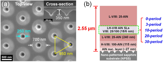
As shown in Fig. 1(a), the NPSS exhibited funnel-shaped patterns with top and bottom diameters of 700 and 250 nm, respectively, and a depth of 350 nm. Figure 1(b) shows the AlN structures with a total thickness of 2.55 μm, the structures of which have the same buffer layers consisting of an approximately 27-nm-thick AlN nucleation layer, a 115-nm-thick high V/III (H-V/III = 100) AlN, and a 240-nm-thick low V/III (L-V/III = 25) AlN. Following the 0∼30 period LH-V/III (alternation of H- and L-V/III) AlN SLs and an L-V/III AlN top layer were deposited onto the buffer layers, respectively. Meanwhile, the thickness of the L-V/III AlN top layer increased from 2.16 to 1.45 μm with an increase in the SL period from 0 to 30.
Figure 1.
(a) Features of NPSS and (b) epitaxial structures of AlN with 0–30 period SLs.
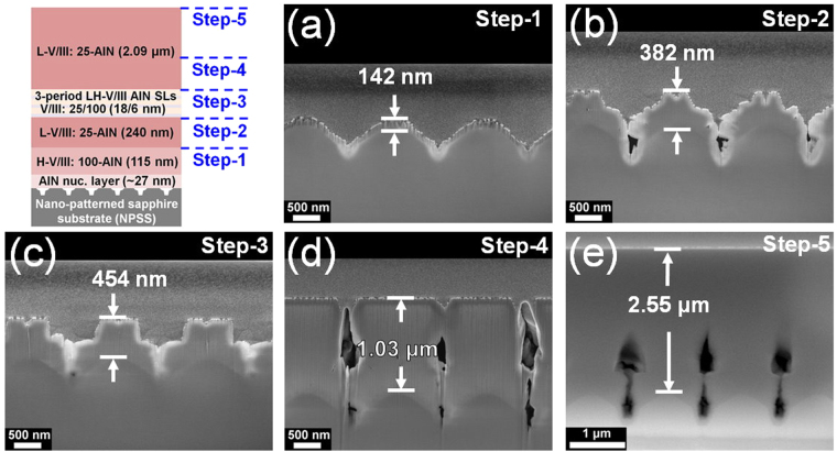
To understand the growth evolution of the AlN structure deposited on NPSS, the cross-sectional field emission scanning electron microscopy (FESEM) images of AlN with 3-period SLs recorded at various growth steps are shown in Fig. 2. At the growth step-1 (Fig. 2(a)), the AlN layer covered all of the NPSS, even the patterned regions, because of the high sticking coefficient of the Al adatoms13. From step-2 to step-3 (Fig. 2(b) and (c), respectively), the AlN epilayer was grown along the c-plane direction despite the increase in the lateral growth rate of the layer. At growth step-4 (Fig. 2(d)), the epilayer coalesced, and some holes were observed on the patterned regions. These results indicated that the growth evolution of the AlN epilayer is dominated by epitaxial lateral overgrowth (ELOG). Finally, the flat AlN epilayer was observed at growth step-5 (Fig. 2(e)). Notably, some key-holes were formed on the patterned regions, which could decrease the tensile stress caused by the lattice mismatch between the AlN layer and sapphire. Figure 3 shows the further evaluation of the crystallinity of the AlN epilayers in terms of the full width at half maximum (FWHM) values for (0002) and (10ī2) for the AlN structure from the growth step-2 to step-5. The (0002) and (10ī2) FWHM values decreased as a function of the growth steps. The FWHM value of (0002) decreased from 1178 to 415 arcsec, while that of (10ī2) decreased from 1678 to 714 arcsec. The (0002) FWHM corresponded to screw dislocations, while the (10ī2) FWHM corresponded to the edge and mixed dislocations14. In this study, the growth evolution of the epilayer was dominated by ELOG as shown in the FESEM images in Fig. 2. The decrease in both (0002) and (10ī2) FWHM values was related to the fact that ELOG can assist in the elimination of dislocations by bending or combining with each other.
Figure 2.
Cross-sectional FESEM images of the AlN structure grown at (a) step-1, (b) step-2, (c) step-3, (d) step-4, and (e) step-5.
Figure 3.
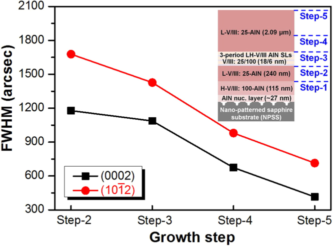
FWHM values of the AlN structure at various growth steps.
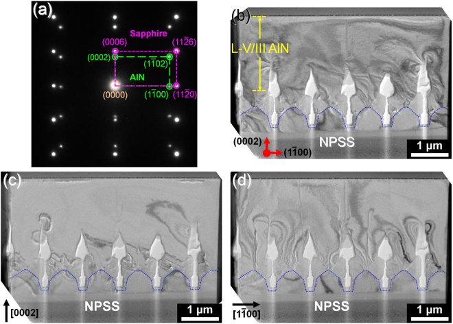
Figure 4 shows the epitaxial relationship and dislocation behavior of AlN grown on NPSS. The diffraction pattern at the AlN/NPSS interface (Fig. 4(a)), where the relationship is AlN (0002)||sapphire (0006) and AlN (1ī00)||sapphire (11–20), indicating that the AlN epilayer exhibits a preferred (0002) orientation (along the c-plane direction). In our previous research10, it can clearly indicate that the insertion of AlN SLs into the AlN epilayer (on flat sapphire) is beneficial to decrease the dislocation density. Without inserting the AlN SLs, the dislocations can easily propagate from the AlN/sapphire interface to the surface of AlN epilayer. However, after inserting the AlN SLs into the AlN epilayer, the dislocation propagation can be eliminated efficiently. This is why the insertion of AlN SLs was used during the growth of AlN epilayer on NPSS. Actually, the insertion of AlN SLs is also helpful to reduce the dislocation density of the AlN epilayer on NPSS, as discussed in Fig. 5(a). The cross-sectional bright-field transmission electron microscopy (TEM) image of the AlN (Fig. 4(b)) revealed only a few dislocations propagating to the layer surface. The total dislocation density near the layer surface was estimated to be approximately 1 × 108 cm−2, suggesting that most dislocations are eliminated by inducing the SL structure and ELOG. The TEM images shown under a two-beam condition are utilized to distinguish the screw, edge, and mixed dislocations, as shown in Fig. 4(c) and (d). The Burgers vector (b) of the screw dislocation is b = <0001> and that of edge dislocations is b = 1/3 <1ī20>15. Based on the invisible criterion g·b = 0, the screw and edge dislocations were observed along g = 0002 and g = 1ī00, respectively. Meanwhile, mixed dislocations were observed at g = 0002 and g = 1ī00. Notably, the number of edge dislocations was greater than the screw dislocations near the layer surface, corresponding to the (0002) FWHM being less than the (10ī2) FWHM.
Figure 4.
(a) Diffraction pattern of the AlN/sapphire interface. (b) Cross-sectional bright-field TEM image of the AlN structure/NPSS. TEM images with a two-beam condition along (c) g = 0002 and (d) g = 1–100.
Figure 5.
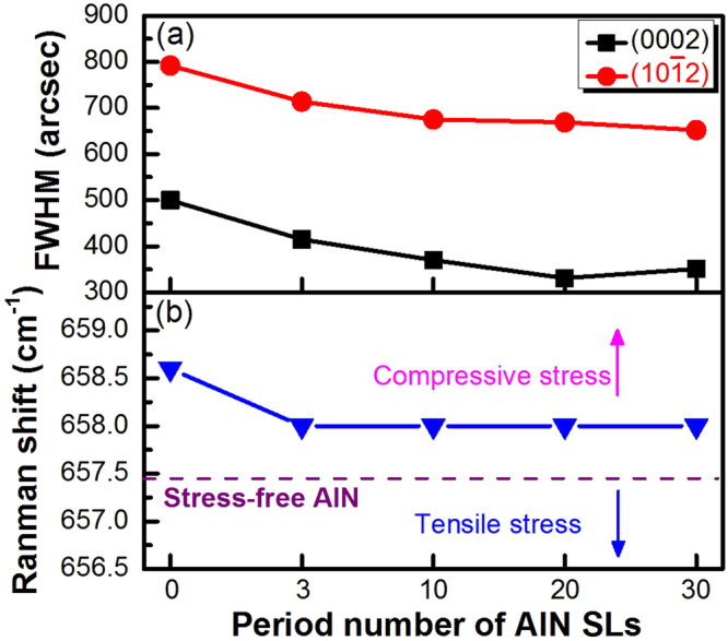
(a) FWHM values and (b) Raman shift of AlN with 0–30 period SL structures.
To enhance the crystal quality of the AlN structure grown on NPSS, the period number of the SLs was optimized. In Fig. 5(a), both (0002) and (10ī2) FWHM values gradually reduced with the increase in the SL period from 0 to 30. Moreover, the decrease in the FWHM values attained stability at SL period greater than 10. Before inserting the AlN SLs, the (0002) and (10ī2) FWHM values of the AlN epilayer were 500 and 792 arcsec, respectively. In the SL periods of 0–30, the lowest (0002) FWHM value of 331 arcsec and (10ī2) FWHM value of 652 arcsec were obtained by utilizing the 20-period SLs. These results indicated that the SLs can effectively assist in the elimination of dislocations. The screw and edge dislocation densities (Dscrew and Dedge) can be derived from the following equations: Dscrew = β(002)/9b2 screw and Dedge = β(102)/9b2 edge 16. In these two equations, β(002) and β(102) represent the FWHM values of AlN(0002) and AlN(10ī2), respectively. Additionally, b is the Burger vector length. Here, bedge and bscrew are 0.3189 and 0.5185 nm, respectively. Via our calculations, the screw and edge dislocation densities of the AlN epilayer without inserting the AlN SLs are 5.02 × 10⁸ and 2.61 × 1010 cm−2, respectively. With the insertion of the 20-period SLs, these two dislocation densities can be reduced to 2.20 × 10⁸ and 2.01 × 1010 cm−2, respectively. In comparison to the dislocation density (1 × 108 cm−2) from the TEM image (Fig. 4(b)), these calculated dislocation densities are higher. This is attributed that the estimation of dislocation density via the TEM result is observed near the epilayer surface. It can be found that the reduction of screw dislocation density is more obvious when the technique of SLs combined with NPSS is used. In addition to AlN crystallinity, the stress management of AlN is crucial for the fabrication of DUV-LEDs. Hence, the residual stress of AlN with 0∼30 period SL structures is estimated by Raman measurement (Fig. 5(b)). The frequency of the E2 high phonon mode was located at 658.6 cm−1 for AlN with 0-period SLs and at 658 cm−1 for AlN with 3∼30 period SL structures. For stress-free AlN17,18, the frequency was located at 657.4 cm−1. Notably, the AlN epilayers with 0∼30 period SL structures exhibited a higher frequency compared to the stress-free frequency, which is indicative of compressive stress. Moreover, the in-plane compressive stress (σ) of AlN can be evaluated by the following equation17,18:
Here, C is the biaxial strain coefficient (3 cm−1/GPa)19, and ωE2 (high) and ω0 are the frequencies of the E2 high phonon mode for AlN with SL structures and stress-free AlN, respectively. Hence, the compressive stress of AlN with 0 period and 3∼30 period SL structures are 0.4 and 0.2 GPa, respectively. This result indicated that the compressive stress state is related to the existence of SLs on the patterned regions. A similar result has been reported by Dong et al.17, wherein the AlN epilayer with a frequency of 658.7 cm−1 and a compressive stress of 0.43 GPa are obtained for AlN grown on NPSS at a temperature of 1200 °C. In this study, the AlN with SL structures grown under a low temperature of 1130 °C revealed a lower compressive stress.
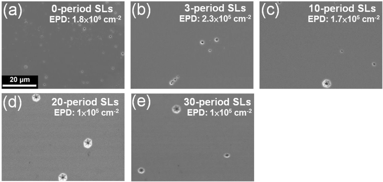
To realize the density of the dislocations that have propagated to the epilayer surface, the etching pit density (EPD) of AlN with SL periods 0∼30 was estimated (Fig. 6). After etching in the KOH solution, the difference in the etching rates of the screw, edge, and mixed dislocations led to etching pits with different pit sizes. Kitagawa et al. have suggested that the smallest etching pits correspond to edge-type dislocations, while the largest hexagonal pits correspond to screw or mixed type dislocations20. In this study, edge-type dislocations decreased with the increase in the SL period from 0 to 30 owing to dislocation elimination (Fig. 6(a–e)). Overall, the EPD decreased from 1.8 × 10⁶ to 1 × 105 cm−2 with the increase in the SL period from 0 to 30. In contrast to the EPD of 2 × 106 cm−2 reported by Kim et al.7 and the EPD of 1 × 106 cm−2 reported by Tran et al.21, the AlN with 20∼30 period SLs revealed an ultra-low EPD value of 1 × 105 cm−2 in this study, indicating that the increase in the SL period effectively assists in the decrease of the dislocation density. This result corresponds with the FWHM values of AlN along (0002) and (10–12). To achieve a high relative IQE of the AlGaN MQW structure, the AlN with 20-period SLs was utilized as a growth template.
Figure 6.
Surface morphology images of AlN with (a) 0, (b) 3, (c) 10, (d) 20, and (e) 30 period SL structures after etching in a KOH solution.
To confirm the defect density of the AlN template on the relative IQE of AlGaN-based MQWs, 280-nm-MQW structures were prepared on AlN both without and with 20-period SLs, which are denoted as structures A and B, respectively. For structure A (shown in Fig. 7(a)), the emission wavelength of the MQWs was observed at 276 nm for RT and 272 nm for LT (10 K). A clear shoulder peak at 260 nm for the LT was caused by the Al0.6Ga0.4N barrier layer and buffer layer. If the IQE of the MQWs under the LT condition was assumed to be 100%, the relative IQE of structure A at RT can be evaluated as 22.4%. In contrast to structure A, structure B exhibited narrower emission peaks at 281 nm for RT and 279 nm for LT (Fig. 7(b)). The relative IQE of structure B was estimated as 85%, indicating that the 280-nm-MQW structure grown on a low-defect-density AlN template effectively enhances the relative IQE. By comparing the RT-PL characteristics of AlGaN MQWs on AlGaN/AlN templates without and with the AlN SLs (Fig. 7(a) and (b)), we can observe that the main emission wavelengths of these two MQWs were centered at 276 and 281 nm, respectively. The composition-pulling effect can be used to realize the result. Without inserting the AlN SLs, there existed a relatively larger compressive stress in the wells. This would result in the composition tendency of AlGaN wells towards higher Al content to minimize the lattice mismatch22. However, as the AlN SLs were inserted into the AlN epilayer, the compressive stress in the wells became smaller, leading to the lower Al content in AlGaN wells. This is why the AlGaN MQWs on AlGaN/AlN template without inserting the AlN SLs have a shorter emission wavelength. In addition, the other interesting phenomenon was also observed in PL results. Comparing the main RT-PL peaks of these two structures, the AlGaN MQWs on AlGaN/AlN template without inserting the AlN SLs possessed an apparent larger FWHM value (149.9 nm) than that with inserting the AlN SLs (14.1 nm). There could be two reasons to explain it. The first reason is the formation of quantum-confined Stark effect (QCSE) in the structure without the AlN SLs, which causes the band tilt23,24. Second, due to the higher defect density of AlN epilayer without the insertion of AlN SLs, the quality of the AlGaN MQWs was lower. Thus, the FWHM value of RT-PL peak for the structure A was apparently large. In general, the QCSE is related to the red-shift of emission peak. However, compared to the PL characteristic of the structure B (with inserting the AlN SLs), the blue-shift phenomenon occurred in the structure A. We can speculate that this shift of emission peak is mainly dominated by the composition-pulling effect. Besides, the differences between emission peaks measured at RT and LT for the AlGaN MQWs on AlGaN/AlN templates without and with inserting the AlN SLs were measured to be 4 and 2 nm, respectively. The larger shift of PL peak in the structure A is possible owing to its higher compressive stress in the wells measured at RT. On the other hand, the relative IQE values obtained from previous studies as well as in this study are summarized in Table 1. As shown in Table 1, Hirayama et al. have obtained a high relative IQE of 86% using the InxAlyGa1−x−yN/InxAlzGa1−x−zN MQWs. For the AlGaN-based MQWs, the relative IQE of the listed research results is shown to be around 43–69%. For these previous studies, the AlN templates were prepared at a high growth temperature (≥1250 °C). Herein, a high relative IQE of 85% for 280 nm AlGaN-based MQWs was achieved by using an AlN template grown under a low growth temperature (1130 °C) and it has hardly ever been reported for AlGaN one. Therefore, the low-EPD AlN templates designed by defect reduction engineering demonstrate high potential for high-IQE DUV-LEDs applications.
Figure 7.
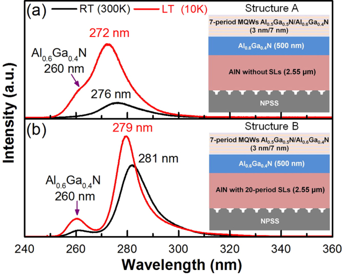
PL spectra of (a) structure A and (b) structure B under RT and LT.
Table 1.
Summary of wavelength, MQWs structure, and relative IQE from previous research results and this study.
| Wavelength | MQW structure (Well/Barrier) | Condition of PL measurement at RT/LT | Relative IQE IRT/ILT | Authorref. |
|---|---|---|---|---|
| 247 nm | AlxGa1−xN/AlN | 300 K/8.5 K | 69% | Banal et al.12 |
| 250 nm | Al0.7Ga0.3N/AlN | 285 K/12 K | 50% | Bhattacharyya et al.25 |
| 278 nm | AlxGa1−xN/AlyGa1−yN | 300 K/14 K | 55% | Shatalov et al.9 |
| 280 nm | AlxGa1−xN/AlyGa1−yN | 300 K/77 K | 50% | Hirayama et al.11 |
| InxAlyGa1−x−yN/InxAlzGa1−x−zN | 86% | |||
| 283 nm | Al0.4Ga0.6N/Al0.5Ga0.5N | 300 K/10 K | 43% | Dong et al.17 |
| 281 nm | Al0.5Ga0.5N/Al0.6Ga0.4N | 300 K/12 K | 85% | NCHU |
Conclusions
The low-defect-density AlN templates were successfully fabricated under a low growth temperature (1130 °C) to achieve high-IQE MQWs. From the FESEM analysis of the growth evolution of AlN with 3-period SLs grown on NPSS, the growth of the AlN layers was dominated by ELOG. Meanwhile, some key-holes were observed upon the pattern regions. These key-holes could be relaxed the tensile stress, related to the lattice mismatch between AlN and sapphire. Besides, the (0002) and (10ī2) FWHM values decreased with the increase in the growth step because of the elimination of dislocations. From the TEM analysis, the ELOG and induction of SLs can assist in the elimination of most dislocations, with only a few of the dislocations propagating to the layer surface. As a result, the total dislocation density of AlN with 3-period SLs is estimated to be approximately 1 × 108 cm−2. The further enhancement of the AlN crystal quality was achieved by the increase in the SL period (0∼30), and the AlN structure with 20-period SLs exhibited the lowest (0002) FWHM value of 331 arcsec and (10ī2) FWHM value of 652 arcsec, as well as an ultra-low EPD of 1 × 105 cm−2. Therefore, the AlN structure with 20-period SLs is selected as a growth template for preparing the AlGaN MQWs with an emission wavelength of 280 nm. Notably, the relative IQE dramatically enhanced by approximately four times (from 22.8% to 85%) for the growth of 280-nm-MQWs on the AlN template with 20-period SLs. These results exhibit that the presented the AlN templates by defect engineering can provide an alternate approach in developing high-efficient DUV-LEDs.
Methods
In this study, the AlN epitaxial structures were grown on 2-inch NPSS by utilizing Aixtron MOCVD. The growth temperature, pressure, and V/III ratio of the AlN nucleation layer were 1000 °C, 100 mbar, and 800, respectively. Other layers were grown at 1130 °C under a pressure of 100 mbar. The crystallinity of all of the AlN epilayers was measured by X-ray diffraction. The growth evolution and dislocation behavior of the AlN epilayers were observed by FESEM and TEM. The residual stress of the AlN layers was estimated by Raman measurement. The EPD of AlN was obtained by etching in a 45 wt% KOH solution at 75 °C for 4.5 min. To further verify the effect of the defect density of the AlN template on the relative IQE of 280-nm-MQWs, an Al0.6Ga0.4N buffer layer with a thickness of 500 nm and 7-period Al0.5Ga0.5N (3 nm)/Al0.6Ga0.4N (7 nm) MQWs were prepared on AlN both with and without 20-period LH-V/III AlN SLs. The relative IQE of 280-nm-MQWs was estimated by PL measurement with an excitation laser of 213 nm under RT and LT, following the relative formula IQE = IRT/ILT.
Acknowledgements
This study was supported by the Ministry of Science and Technology (Taiwan, R.O.C.) under the Contract No. 104-2221-E-005-036-MY3.
Author Contributions
T.Y.W. and D.S.W. proposed the epitaxial structure and wrote the manuscript. T.Y.W. and C.T.T. contributed to the MOCVD growth, material characterization and data analysis. C.F.L. contributed to the photoluminescence measurements and characterization. D.S.W. supervised the project.
Competing Interests
The authors declare that they have no competing interests.
Footnotes
Publisher's note: Springer Nature remains neutral with regard to jurisdictional claims in published maps and institutional affiliations.
References
- 1.Mellqvist J, Rosen A. DOAS for flue gas monitoring—temperature effects in the UV/visible absorption spectra of NO, NO2, SO2, and NH3. J. Quant. Spectrosc. Radiat. Transf. 1996;56:187–208. doi: 10.1016/0022-4073(96)00042-8. [DOI] [Google Scholar]
- 2.Imura M, et al. Dislocations in AIN epilayers grown on sapphire substrate by high-temperature metal-organicvapor phase epitaxy. Jpn. J. Appl. Phys. 2007;46:1458–1462. doi: 10.1143/JJAP.46.1458. [DOI] [Google Scholar]
- 3.Kneissl M, et al. Advances in group III-nitride-based deep UV light-emitting diode technology. Semicond. Sci. Technol. 2011;26:014036. doi: 10.1088/0268-1242/26/1/014036. [DOI] [Google Scholar]
- 4.Miyake H, et al. Annealing of an AlN buffer layer in N2–CO for growth of a high-quality AlN film on sapphire. Appl. Phys. Express. 2016;9:025501. doi: 10.7567/APEX.9.025501. [DOI] [Google Scholar]
- 5.Hirayama H, Yatabe T, Noguchi N, Ohashi T, Kamata N. 231–261 nm AlGaN deep-ultraviolet light-emitting diodes fabricated on AlN multilayer buffers grown by ammonia pulse-flow method on sapphire. Appl. Phys. Lett. 2007;91:071901. doi: 10.1063/1.2770662. [DOI] [Google Scholar]
- 6.Yan J, et al. AlGaN-based deep-ultraviolet light-emitting diodes grown on High-quality AlN template using MOVPE. J. Cryst. Growth. 2015;414:254–257. doi: 10.1016/j.jcrysgro.2014.10.015. [DOI] [Google Scholar]
- 7.Kim J, Pyeon J, Jeon M, Nam O. Growth and characterization of high quality AlN using combined structure of low temperature buffer and superlattices for applications in the deep ultraviolet. Jpn. J. Appl. Phys. 2015;54:081001. doi: 10.7567/JJAP.54.081001. [DOI] [Google Scholar]
- 8.Zhang L, et al. High-quality AlN epitaxy on nanopatterned sapphire substrates prepared by nano-imprint lithography. Sci. Rep. 2016;6:35934. doi: 10.1038/srep35934. [DOI] [PMC free article] [PubMed] [Google Scholar]
- 9.Shatalov M, et al. AlGaN Deep-Ultraviolet Light-Emitting Diodes with External Quantum Efficiency above 10% Appl. Phys. Express. 2012;5:082101. doi: 10.1143/APEX.5.082101. [DOI] [Google Scholar]
- 10.Wang TY, Liang JH, Fu GW, Wuu DS. Defect Annihilation Mechanism of AlN Buffer Structures with Alternating High and Low V/III Ratios by MOCVD. CrystEngComm. 2016;18:9152–9159. doi: 10.1039/C6CE02130A. [DOI] [Google Scholar]
- 11.Hirayama H, et al. 222–282 nm AlGaN and InAlGaN-based deep-UV LEDs fabricated on high-quality AlN on sapphire. Phys. Status Solidi A. 2009;206:1176–1182. doi: 10.1002/pssa.200880961. [DOI] [Google Scholar]
- 12.Banal RG, Funato M, Kawakami Y. Extremely high internal quantum efficiencies from AlGaN/AlN quantum wells emitting in the deep ultraviolet spectral region. Appl. Phys. Lett. 2011;99:011902. doi: 10.1063/1.3607306. [DOI] [Google Scholar]
- 13.Sun X, et al. In situ observation of two-step growth of AlN on sapphire using high-temperature metal–organic chemical vapour deposition. CrystEngComm. 2013;15:6066–6073. doi: 10.1039/c3ce40755a. [DOI] [Google Scholar]
- 14.Chierchia R, et al. Microstructure of heteroepitaxial GaN revealed by x-ray diffraction. J. Appl. Phys. 2003;93:8918–8925. doi: 10.1063/1.1571217. [DOI] [Google Scholar]
- 15.Imura M, et al. Annihilation mechanism of threading dislocations in AlN grown by growth form modification method using V/III ratio. J. Cryst. Growth. 2007;300:136–140. doi: 10.1016/j.jcrysgro.2006.11.013. [DOI] [Google Scholar]
- 16.Wang TY, Ou SL, Horng RH, Wuu DS. Growth evolution of SixNy on the GaN underlayer and its effects on GaN-on-Si (111) heteroepitaxial quality. CrystEngComm. 2014;16:5724. doi: 10.1039/C3CE42638F. [DOI] [Google Scholar]
- 17.Dong P, et al. AlGaN-based deep ultraviolet light-emitting diodes grown on nano-patterned sapphire substrates with significant improvement in internal quantum efficiency. J. Cryst. Growth. 2014;395:9–13. doi: 10.1016/j.jcrysgro.2014.02.039. [DOI] [Google Scholar]
- 18.Prokofyeva T, et al. Vibrational properties of AlN grown on (111)-oriented silicon. Phys. Rev. B. 2001;63:125313. doi: 10.1103/PhysRevB.63.125313. [DOI] [Google Scholar]
- 19.Sarua A, Kuball M, Nostrand JEV. Deformation potentials of the E2 high phonon mode of AlN. Appl. Phys. Lett. 2004;85:2217–2219. doi: 10.1063/1.1793338. [DOI] [Google Scholar]
- 20.Kitagawa S, Miyake H, Hiramatsu K. High-quality AlN growth on 6H-SiC substrate using three dimensional nucleation by lowpressure hydride vapor phase epitaxy. Jpn. J. Appl. Phys. 2014;53:05FL03. doi: 10.7567/JJAP.53.05FL03. [DOI] [Google Scholar]
- 21.Tran BT, et al. Performance Improvement of AlN Crystal Quality Grown on Patterned Si(111) Substrate for Deep UV-LED Applications. Sci. Rep. 2016;6:35681. doi: 10.1038/srep35681. [DOI] [PMC free article] [PubMed] [Google Scholar]
- 22.Li X, et al. AlGaN-based MQWs grown on a thick relaxed AlGaN buffer on AlN templates emitting at 285 nm. Opt. Mater. Express. 2015;5:380–392. doi: 10.1364/OME.5.000380. [DOI] [Google Scholar]
- 23.Tamulaitis G. Ultraviolet light emitting diodes. Lithuanian J. Phys. 2011;51:177–193. doi: 10.3952/lithjphys.51307. [DOI] [Google Scholar]
- 24.Li L, Miyachi Y, Miyoshi M, Egawa T. Enhanced Emission Efficiency of Deep Ultraviolet Light-Emitting AlGaN Multiple Quantum Wells Grown on an N-AlGaN Underlying Layer. IEEE PHOTONICS J. 2016;8:1601710. [Google Scholar]
- 25.Bhattacharyya A, et al. Deep ultraviolet emitting AlGaN quantum wells with high internal quantum efficiency. Appl. Phys. Lett. 2009;94:181907. doi: 10.1063/1.3130755. [DOI] [Google Scholar]


