Abstract
Nanosheet Ca2Nb3O10 (CNOns) layers were deposited on ultralow expansion glass substrates by the Langmuir–Blodgett method to obtain preferential (001)-oriented growth of Pb(Zr0.52Ti0.48)O3 (PZT) thin films using pulsed laser deposition (PLD) to enhance the ferroelectric and piezoelectric properties of the films. The PLD deposition temperature and repetition frequency used for the deposition of the PZT films were found to play a key role in the precise control of the microstructure and therefore of the ferroelectric and piezoelectric properties. A film deposited at a high repetition frequency has a columnar grain structure, which helps to increase the longitudinal piezoelectric coefficient (d33f). An enhanced d33f value of 356 pm V–1 was obtained for 2-μm-thick PZT films on CNOns/glass substrates. This high value is ascribed to the preferential alignment of the crystalline [001] axis normal to the substrate surface and the open columnar structure. Large displacement actuators based on such PZT films grown on CNOns/glass substrates should be useful in smart X-ray optics applications.
Keywords: piezoelectric films, nanosheets, ultralow expansion glass, microstructure, ultrahigh piezoelectricity
Introduction
Recently there has been an increased demand for high performance piezoelectric and ferroelectric thin films for sensors and actuators, such as the transparent touch panel1,2 and adaptive optics for telescopes.3 For these applications, lead zirconate titanate (PZT) thin films have received much attention because of the strong intrinsic piezoelectric and ferroelectric properties.
In a previous paper we showed that the use of Ca2Nb3O10 nanosheets (CNOns) as a seed layer is a promising route for achieving highly (001)-oriented, textured PZT films on Si substrates.4 The high crystalline quality of the PZT films can significantly improve the performance of envisaged microelectromechanical systems (MEMS) devices. However, the use of Si substrates limits the applications of PZT films for optical and electro-optic applications because Si is not transparent.5 Similar to Si in the semiconductor industry, transparent glass plays a very important role in optical systems. Especially the very low thermal expansion of ultralow expansion (ULE) glass has made it the material of choice for X-ray optics applications, such as lightweight mirror blanks for astronomical telescopes, interferometry space satellite applications, and extreme UV mirrors for lithography.6−9
There have been some studies on the fabrication and optimization of PZT films on glass substrates. In order to fabricate dense and uniform PZT films on such substrates, conductive metal oxide LaNiO3 (LNO) was developed as a buffer layer.10 The application of nanosheets as a seed layer on glass substrate has been of great interest for the orientation control of perovskite films. Kikuta et al.11 and Bayraktar et al.12 deposited highly (001)-oriented PZT films on glass substrates, using CNOns as a buffer layer. They reported improved ferroelectric and piezoelectric properties in these films. However, the observed piezoelectric coefficients were much lower (∼100 pm V–1) than those of the respective bulk PZT ceramics (223 pm V–1),13 which was explained by the substrate clamping of the film.14 Recently, Bayraktar et al.9 observed a very high piezoelectric coefficient (d33 = 250 pm V–1) in 2-μm-thick PZT films on CNOns/ULE glass, using LaNiO3 electrodes. This observation is of great interest for smart X-ray optics applications.
The control of the microstructure and orientation of the PZT film is very important for device performance. In film growth processes, the microstructure of a film is usually determined by the nucleation and initial growth phase. The former is mainly controlled by the substrate used, such as crystallinity, surface orientation, and lattice mismatch, while the latter is usually controlled by the process conditions. Therefore, for the complete control of a film microstructure, it is required to understand the effects of both substrate and processing parameters on the nucleation and growth of the film. This eventually will provide ways to improve the device performance. So far there have been many studies on the effect of deposition conditions, such as deposition temperature and deposition pressure, on the microstructure and the ferroelectric and the piezoelectric properties of PZT films prepared by the pulsed laser deposition (PLD) technique.15−19 It was found that the deposition conditions play an important role in the nucleation and formation of the perovskite phase.20 For the deposition of PZT films, especially on substrate materials with a low phase transition temperature (e.g., glass), one of the most important problems is the deposition temperature. This temperature not only determines the initial growth of a film, but also its subsequent growth and therefore its microstructure and properties. The most practical MEMS device structures available today are probably piezoelectric MEMS. However, the high process temperature is an obstacle for integration of the MEMS device directly onto a complementary metal-oxide semiconductor (CMOS) device. A CMOS device, especially on a glass substrate, due to its nature, can only withstand a process temperature of at the most 500 °C. The typical crystallization/deposition temperature of PZT films is in the range 550–600 °C for sputtering,21,22 and 600–650 °C for sol-gel deposition.23,24 With PLD a smooth film surface can be obtained by varying the number of laser pulses per second, keeping the amount of material deposited per shot constant.25 In that case a lower deposition rate or a longer growth time (a lower laser pulse repetition frequency) for a fixed pulse intensity (laser power density) means that the nuclei have more time to ripen, and one expects the film to evolve into a smooth surface with large, flat areas.17 However, there are hardly any studies on the effect of laser pulse rate on the growth and properties of PZT films. Guan et al.17 used a Monte Carlo computational model to study the influence of the pulse rate on the island density and film morphology in the early phase of PLD growth. The computational results indicated that more and smaller sized islands are formed at higher repetition rates, and the reduced island size enhances the diffusion of adatoms resulting in a smoother film surface.
In this paper, we report on the fabrication of 2-μm-thick PZT films using pulsed laser deposition (PLD) with high longitudinal piezo-responses on ULE glass substrates with CNOns buffer layers at deposition temperatures as low as 450 °C. The relationship between the deposition conditions, the microstructural properties, and the piezoelectric properties of in situ PZT films deposited by pulsed laser deposition was investigated. Moreover, the dependence of piezoelectric properties on nanosheet buffer-layer and substrate-type is discussed.
Experimental Section
The concept of growth and control of the growth direction of perovskite layers on nanosheets was introduced by Kikuta et al.11 and demonstrated with PLD-grown epitaxial films on CNOns and TiOns by Nijland et al.26 The backbone of CNOns consists of corner-sharing NbO6 octahedra with a (001) surface plane and a pseudocubic lattice constant of ap = 3.86 Å. TiOns consists of side-sharing TiO6 octahedra creating a hexagonal surface plane with in-plane lattice constants a = 3.76 Å and b = 2.97 Å, compatible with (110)-oriented growth of perovskites. The thickness of the nanosheet is a few nanometers.
Synthesis Nanosheets
Ca2Nb3O10 (CNOns) and Ti0.87O2 (TiOns) nanosheets were fabricated by exfoliation of layered protonated titanate (H1.07Ti1.73O4·H2O) and protonated calcium niobate (HCa2Nb3O10·1.5H2O) followed by the Langmuir–Blodgett (LB) deposition method. The details of the flux-synthesized, layered precursor K0.8[Ti1.73Li0.27O4] and the solid state synthesized, layered precursor KCa2Nb3O10 and their protonation processes can be found in previous reports.27−29 The AFM images of a monolayer CNOns on glass and Si substrates as well as on TiOns on glass substrate, are shown in Figure S1 (Supporting Information, SI).
Pulsed Laser Deposition
Pb(Zr0.52Ti0.48)O3 (PZT) thin films with a thickness of about 2-μm (±0.05 μm) were grown on 200 nm-thick LaNiO3 (LNO) electrode buffered glass, CNOns/glass, TiOns/glass, and CNOns/Si substrates with pulsed laser deposition (PLD) using a KrF excimer laser source (Lambda Physik, 248 nm wavelength). The deposition conditions of the PZT films were laser repetition frequency 10–50 Hz, substrate temperature 450–600 °C, energy density 2.5 J cm–2, and oxygen pressure 0.1 mbar. The deposition conditions were 4 Hz, 600 °C, 2.5 J cm–2, and 0.1 mbar O2 for the LNO electrodes. In the study of the effect of deposition temperature on the properties of PZT films, the LNO electrode was deposited at the same temperature as the PZT film. All layers were deposited successively without breaking the vacuum. After deposition, the films were cooled down to room temperature in a 1 bar oxygen atmosphere at a ramp rate of 8 °C minute–1.
Analysis and Characterization
The crystal structure of the thin films was analyzed by X-ray diffraction θ–2θ and omega scans (XRD, Philips X’Pert X–ray diffractometer). The surface morphology and microstructure were analyzed using atomic force microscopy (AFM: Bruker Dimension Icon), high-resolution scanning electron microscopy (HRSEM: Zeiss–1550), and high-resolution transmission electron microscopy (TEM, Philips CM300ST–FEG). For electrical measurements, the samples with 200 nm-thick LNO top-electrodes were used. 300 × 300 μm2 capacitors were patterned by a standard photolithography process and structured by argon-beam etching of the top-electrodes and wet-etching (HF-HCl solution) of the PZT films (see Figure S2). The polarization hysteresis (P–E) loop measurements were performed with the ferroelectric mode of the aixACCT TF-2000 Analyzer using a triangular ac-electric field of ±200 kV cm–1 at 1 kHz scanning frequency. The effective piezoelectric small-signal coefficient (d33f) and large-signal strain (S) of the piezoelectric thin-film capacitors was measured using a double-beam laser interferometer (aixDBLI) method with a minimum resolution of 0.2 pm. The d33f values were obtained from d33f–E loops measured at increasing cycling intervals at ±200 kV cm–1 and 1 kHz frequency.
Results and Discussion
Effect of Deposition Conditions
Two series of samples were fabricated with the aim to modify the microstructure of the PZT films grown on CNOns/glass substrates by varying respectively the PLD deposition temperature at constant PLD laser pulse frequency (Td = 450, 520, 560, and 600 °C and at 50 Hz) and by varying the laser pulse rate at constant deposition temperature (10, 25, and 50 Hz and with Td = 600 °C). Notable differences in columnar grain growth and film quality were observed, resulting in changes in the polarization and especially the effective, longitudinal piezoelectric constant (d33f) of PZT thin film capacitors.
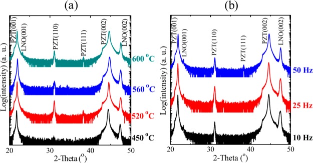
Figure 1a shows the XRD θ–2θ patterns of films deposited at 50 Hz and different substrate temperatures and Figure 1b that of films deposited at 600 °C and varying laser pulse frequency. All PZT films are predominantly (001)-oriented with only minor fractions of (110) and (111) orientations. Note that PZT films with only perovskite phases are obtained even at a deposition temperature as low as 450 °C. This is significantly lower than process temperatures reported in other studies15,30,31 and represents an important advantage for the integration with CMOS devices. The (002) reflection peak of the PZT films was further examined with an X-ray ω-scan (rocking curve), as shown in Figure S3 (SI). The full-width-at-half-maximum (fwhm) values of the PZT films increases only slightly with increasing deposition frequency from 0.52° to 0.67° for 10 and 50 Hz, respectively, and slightly more for deposition temperature decreasing from 600 °C (values in Table 1). Only for the lowest Td = 450 °C does the fwhm increase somewhat more to 1.08°. A lower fwhm value corresponds to a higher quality PZT film, implying that the grains are more aligned.
Figure 1.
XRD θ–2θ scans of 2-μm-thick PZT films grown on LNO/CNOns/glass: (a) Td of 450, 520, 560, and 600 °C and at 50 Hz and (b) 10, 25, and 50 Hz and with Td of 600 °C.
Table 1. Properties of PZT Films on Glass, Si, and STO Substrates with CNO and TiO Nanosheets.
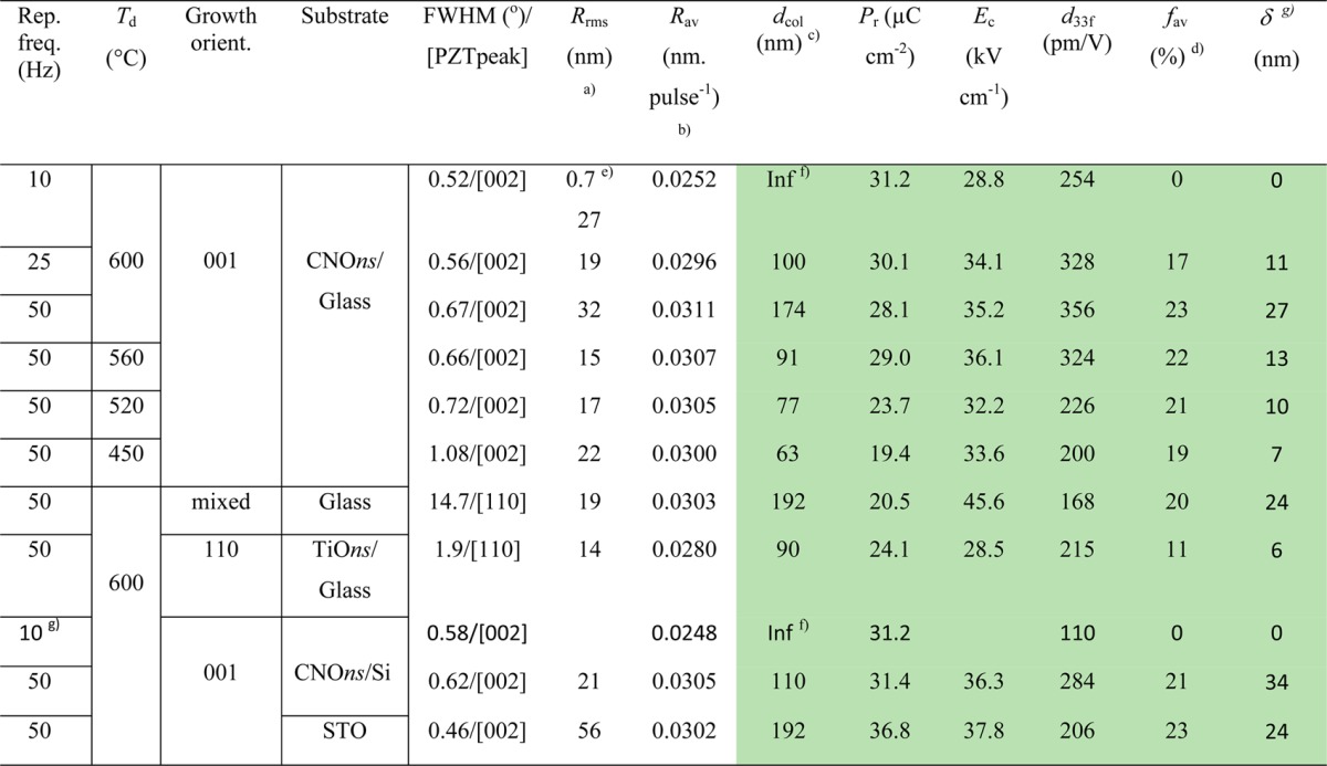
Average root-mean-square roughness (Rrms), determined from AFM images in an average over area of 10 × 10 μm2.
Deposition rate (Rav).
Average grain size (dcol), determined from SEM cross-section.
Average volume void fraction and average grain spacing calculated as in ref (34) from the measured Rav data, assuming that the (10 Hz, 600 °C)-film is 100% dense.
On top of nanosheet.
Film is assumed to be 100% dense.
Estimated from the average deposition rate and the average grain diameter, following the procedure described in ref (34).
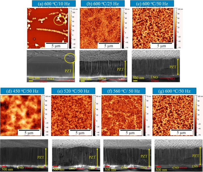
The film morphology and structure were investigated by AFM and cross-sectional SEM as shown in Figure 2. First we discuss the frequency dependence. The film deposited at 600 °C and 10 Hz shows a very dense, structure free film on top of the nanosheets, which is extremely flat. It was shown previously that the observed polycrystalline columnar structure formed along lines arises from the edges of the nanosheets. The average column diameter range from 20 to 30 nm at the bottom to a few 100 nm at the top of the 2-μm-thick film. This structure was ascribed to a different nucleation density and growth at the edges of the nanosheets and the in-plane orientation mismatch of the single crystals grown on top of neighboring nanosheets. The same mechanism was also observed in the PZT films grown on the CNO nanosheets buffered Si substrates, in which the columnar growth was formed on parts of the Si substrate that are not covered by CNO nanosheets.4 For higher laser frequencies, the structure of the film is columnar (Figure 2b,c). The fine columnar structure on the nanosheet is very similar to the columnar structure off the nanosheets, which makes it impossible to distinguish the two orientations from the SEM images. However, the XRD measurements show approximately the same ratio of (001) and non (001)-oriented growths, suggesting that on the nanosheets the growth is still (001)-oriented. The change from the dense structure to the columnar structure on the nanosheets is attributed to a drastic increase in the nucleation density with increasing laser frequency, due to strongly reduced diffusion time for particles arriving on the film surface. This structural change also has a large effect on the surface roughness. It is only 0.7 nm on top of the nanosheet for the film deposited at 10 Hz and 600 °C. It is only due to the columnar growth at the nanosheet edges that the average root-mean-square roughness (Rrms) is fairly large (27 nm, see also Table 1). The Rrms rapidly increases from 19 to 32 nm for the (25 Hz, 600 °C)-film and (50 Hz, 600 °C)-film, respectively. The increased roughness correlates with the larger average columnar grain diameter (dcol), which translates into a higher pyramidal-shape at the top of the layer and thus larger Rrms.
Figure 2.
Surface morphology AFM and cross-sectional SEM images of 2-μm-thick PZT films deposited on LNO/CNOns/glass: (a–c) varying laser frequency and with Td = 600 °C, (d–g) that same for varying deposition temperature (Td) and at 50 Hz laser frequency.
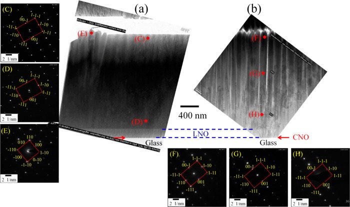
Figure 2d–g shows the surface morphology and structure of films deposited at 50 Hz but at different deposition temperature (Td). With decreasing Td the average grain diameter decreases gradually from 174 nm for the (50 Hz, 600 °C)-film to 63 nm for the (50 Hz, 450 °C)-film. The decreasing column width with decreasing deposition temperature indicates a decreasing lateral growth rate, due to lower surface mobility after the nucleation phase. The surface roughness suddenly decreases from about 32 nm to about 20 nm, when Td is decreased from 600 °C to a lower Td (50 Hz, 560–450 °C)-film. On close examination of the SEM graphs of the top of the grains one can observe a distinct difference between these and the (50 Hz, 560–450 °C)-films. The top of the columns of all films have a pyramidal shape, but the pyramid side surfaces are covered with many small crystallites, smoothing out the sharp features of the pyramidal structure for the latter films. This seems to be the main cause for the sudden reduction in surface roughness with decreasing Td between 600 and 560 °C. Thus, in this temperature interval the nucleation density on the pyramidal side faces is strongly increased, ascribed to the reduced diffusion length in the short time (20 ms) in between laser pulses at these lower temperatures. The cross-sectional TEM image of the PZT film deposited at 10 Hz (Figure 3a), shows the compact grain or “dense” microstructure in the film on the CNOns and the columnar grain on the CNOns edges and in the uncovered glass areas in between the nanosheets. The cross-sectional TEM image of PZT film deposited at 50 Hz also shows the separated columnar microstructure (Figure 3b).
Figure 3.
Cross-sectional TEM images of the 2-μm-thick PZT films grown at (a) 10 Hz and (b) 50 Hz, on LNO/CNO/glass substrates. (C)–(H) SAED patterns taken from the corresponding positions in (a) and (b), respectively.
In a previous paper we described that the columnar grains in films grown along the CNOns edges and in the uncovered Si substrate areas have (110) orientation.4 Therefore, we assume that also in the present case of PZT growth on CNOns on glass, the minor (110)-oriented fraction is due to the growth on the bare glass substrate and along the CNOns edges. In order to verify the origin of the (110) orientation, selected area electron diffraction (SAED) was used. Figure 3(C–E) are the SAED patterns taken from the corresponding positions in the film deposited at 10 Hz, shown in the cross-sectional TEM image Figure 3a. The SAED patterns at the positions C and D correspond to a (110) in-plane direction therefore the growth at these positions is in the [001] direction. In contrast, the SAED of the columnar grains growing at the edge of the nanosheets (position E) have a (100) in-plane orientation, thus the grain growth is in the [110] direction. Although the columnar grains with (110) growth orientation in the gap between nanosheets are also formed in the films deposited at 50 Hz, these (110) grains are difficult to recognize because the microstructure is very similar to that on the nanosheets with (001) orientation. Figure 3(F–H) show the SAED patterns at three positions in a single column on a nanosheet, showing that the growth direction of this column is along [001].
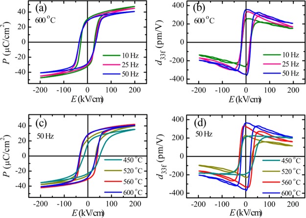
To investigate the effect of the repetition laser frequency and deposition temperature Td on the ferroelectric and piezoelectric properties of PZT films, the P–E and d33f −E hysteresis loops were measured, as shown in Figure 4. The polarization loops for films deposited at 600 °C slightly change by increasing the laser frequency (Figure 4a). The remanent polarization (Pr) of the films deposited at different repetition frequency iesare nearly equal (Table 1), but the slope of the hysteresis loop for increasing applied field increases with decreasing deposition frequency. We think that the value of the remanent polarization and this change in slope are related to a gradual change in the clamping of the grains with laser frequency, but a detailed model that accounts for polarization rotation and extension in relation to more or less clamping to substantiate this is still lacking.
Figure 4.
Ferroelectric polarization (P–E) and piezoelectric (d33f–E) hysteresis loops of 2-μm-thick PZT films deposited on LNO/CNOns/glass (a,b) at varying laser frequency and with Td = 600 °C, and (c,d) the same for varying deposition temperature (Td) and at 50 Hz laser frequency.
The d33f values increase with repetition frequency (Figure 4b), which was previously ascribed to increased declamping of the columns in the film deposited at high repetition frequency. The large d33f values are ascribed to a combination of the intrinsic effect and the extrinsic contribution due to domain switching and polarization rotation. Both intrinsic and extrinsic effects become larger with decreased clamping.32
Applying the same analysis as discussed in ref (32), it is found that with higher laser frequency the film becomes less dense and the columnar grains become more separated. From the measured deposition rate per pulse and the column diameter it is estimated that the average void fraction in the film increases from close to 0% for the 10 Hz-film to 23% for the 50 Hz film, while the average separation between grains increases from 0 to 27 nm (Table 1). Consequently the clamping of the PZT grains is strongly reduced, and the grains may to a large extend be considered as unclamped single crystals. The maximum piezoelectric coefficient is even larger than the theoretical value for a single domain, single crystal (327 pm V–1, Haun et al.).33 The increased value is ascribed to the extrinsic effect of domain wall motion between different polarization domains. This is supported by phase field simulations that have shown that by that mechanism d33f values up to 600 pm V–1 may be possible in unclamped, single crystal PZT with (near-) MPB compositions.34
Figure 4b also indicates that for increasing field d33f rapidly decreases, which in terms of the above explanation implies that the contribution of domain switching and polarization rotation decreases and that the relative contribution of the intrinsic piezoelectric effect becomes larger. Therefore, the d33f value reaches a peak in the low electric field region and gradually decreases as the higher electric field is applied.
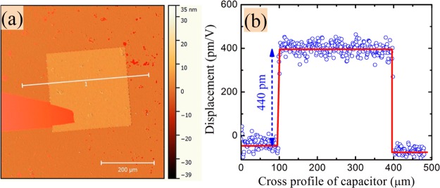
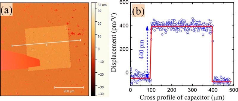
Ferroelectric and piezoelectric properties of PZT thin films have been achieved even at a deposition temperature as low as 450 °C (Figure 4c,d). The polarization decreases with decreasing Td, but only for the lowest deposition temperature is the remanent polarization decreased significantly (Pr is reduced from about 28 to 19 μC cm–2) and the loop has become much more slanted. The effect of decreasing Td on the piezoelectric properties is much stronger: the maximum d33f value decreases from 356 pm V–1 at Td = 600 °C to 200 pm V–1 at Td = 450 °C. We attribute both trends to the change in crystallinity and microstructure with decreasing deposition temperature. Although the void fraction does not change significantly with deposition temperature, the average grain diameter does, and with that the average separation between the grains, which monotonically decreases from about 27 to 7 nm for Td falling from 600 to 450 °C. With decreasing grain separation one may expect that the grains are increasingly connected and then the clamping increases. In general clamping reduces domain wall motion and consequently the extrinsic piezoelectric effect related to domain wall motion, leading to a decrease in the piezoelectric properties. The decrease in the (remanent) polarization at low Td might be due to the degradation of crystallinity (reflected in an increase of the fwhm with decreasing Td), decreasing the amount of switchable polarization. For optical applications, the static piezoelectric displacement of PZT film capacitors is very important. Figure 5a shows the displacement profile of a 2 μm PZT thin film capacitor deposited on CNOns/glass at 50 Hz and 600 °C, measured at an applied DC voltage of 10 V, measured with optical white-light interferometry (WLI) . This is very similar to the way such a device may be used in deformable mirrors to control the wavefront in optical systems. The displacement profile along the trace indicated in Figure 5a is shown in Figure 5b. The average piezoelectric coefficient over the 0–10 V voltage range (this corresponds to 0–50 kV cm–1 applied electric field) is about 440 pm V–1.
Figure 5.
(a) White light interferometer (WLI) measurement and (b) height profile of piezoelectric displacement, of a 2-μm-thick PZT film grown on LNO/CNOns/glass at 50 Hz and 600 °C, measured under a dc-voltage of 10 V.
The strain response of the films was investigated as a function of laser pulse rate. Figure S4 shows the bipolar and unipolar large-signal strain-field hysteresis loops (S–E) for the PZT films grown on CNOns/glass at 600 °C deposition temperature and varying laser frequencies, using a cycle frequency of 1 kHz. Typical butterfly shaped bipolar strain loops are observed. The hysteresis indicates the importance of ferroelectric domain switching and domain wall motion.32 (This is also reflected by the jump to zero strain at E = 0 kV cm–1 in the raising branch of the loop. At this point there is a waiting time in the measurement protocol, before the next cycle is started. During this waiting time the strain is relaxed at constant applied field by continuing domain wall motion.) The strain increases with laser frequency and a maximum strain of about 0.78%, at a driving field of +200 kV cm–1 is obtained for the (50 Hz, 600 °C) film. With increasing strain the slope of the S–E curve decreases, hence the piezoelectric coefficient d33S(E) = (dS/dE)E implies a decreasing piezoelectric effect at high fields. The average piezoelectric strain coefficient (d33S = ΔS/ΔE)) was calculated from the bipolar S–E curve (Figure S4a inset). Table S1 gives the differences in the piezoelectric coefficients measured under the different driving conditions. For the film deposited at 10 Hz, d33f (0 kV cm–1), determined from the small-signal or dc-bias d33f–E hysteresis loop, is about 35% smaller than the large signal value d33S determined from the S–E loop. This difference is even 44% for the films deposited at 25 and 50 Hz. Such a (large) difference was also reported by Berfield et al.23 and attributed to a combination of the active mechanisms that contribute to the piezoelectric response and the way to determine d33 for the different driving cases. For the small-signal piezoelectric (d33f–E) measurement, a low ac-field of 2 kV cm–1 was applied so that the sample response is linear, but the piezoelectric strain (S–E) measurement was performed under an ac-electric field with an amplitude well above the coercive field of the films. The higher extrinsic contribution from domain wall movement and/or electric-field induced domain switching to the response of strain is thought to be the origin of the much higher d33S values determined from the S–E curves than the values from the d33f–E loops.35 However, there is some variation in the slope at E = 0 of the S–E curves for different maximum applied ac fields, and this may affect the calculated d33 value.23 Therefore, the small-signal effective piezoelectric coefficient (d33f) value has been used to compare the piezoelectric properties of PZT grown on different substrates. For actuator applications the maximum achievable strain Smax at maximum applied electric field Emax is the quantity of interest and their ratio Smax/Emax the key figure of merit. Therefore, also the unipolar strain loops of PZT films deposited at different repetition frequencies as a function of unipolar electric field are shown in Figure S4b. The films have a relatively low strain hysteresis (H) of about 6.9–7.5% that slightly decreases above a laser frequency of 25 Hz. Strain hysteresis (related to the piezoelectric loss) was evaluated from the fraction of strain at half-maximum field (see inset in Figure S4b).36 The high piezoelectric strain and low strain hysteresis obtained in this study expand the possibilities for the application of such PZT films in actuator systems.
Effect of Nanosheet Seed Layers
To demonstrate the advantageous effect of a seed layer of nanosheets on the crystalline and electrical properties of PZT films we compared the properties of 2-μm-thick PZT film deposited at a laser frequency of 50 Hz and 600 °C deposition temperature, directly on LNO/glass and LNO/Ti0.87O2 nanosheets on glass (LNO/TiOns/glass) with similar films using LNO/CNOns/glass.
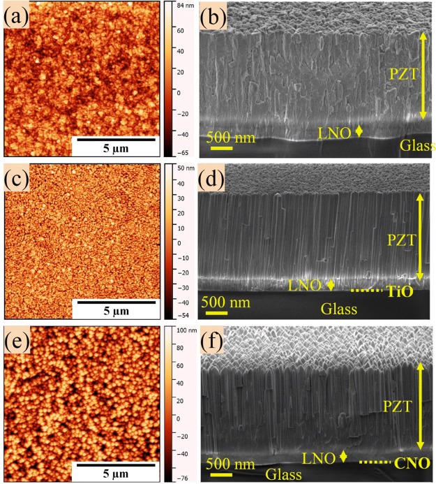
Figure 6 shows the XRD θ–2θ patterns for 2-μm-thick PZT films deposited on LNO/glass, LNO/TiOns/glass, and LNO/CNOns/glass substrates. A predominant (110) orientation (with a minor fraction with (001) orientation) is found for the PZT film on TiOns/glass, while a random orientation is observed for the PZT film deposited on LNO/glass directly. These results indicate that CNOns and TiOns can be utilized to control the orientation of perovskite compounds on glass substrates. The low crystalline quality of the random-oriented PZT film directly grown on glass can also be seen from the large fwhm value of the rocking curve peak (Table 1). The average diameter of the columnar grains in this film is about 192 nm. Note that the columnar grains do not extend from the bottom to the top of the film (Figure 7b) as is the case for the PZT films on LNO/CNOns/glass. In a previous study we have shown that PZT films can be grown on Ti0.87O2 nanosheet buffered Si (TiOns/Si) substrates with a columnar structure.4 Similar to the film grown on TiOns/Si, the film grown on TiOns/glass in this study also has a columnar structure (but more dense and finer than in the case of growth on CNOns/glass) with continuous grains from the bottom electrode to the top of the layer (Figure 7d). The average grain size of about 90 nm in the PZT film on TiOns/glass is much smaller than that on CNOns/glass (174 nm). More information on the grain size and surface roughness of these films is given in Table 1.
Figure 6.
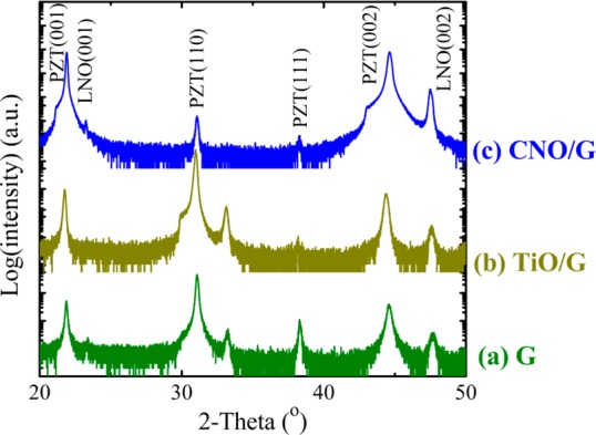
XRD θ–2θ patterns of 2-μm-thick PZT films deposited (at 50 Hz and 600 °C) on LNO buffered (a) glass, (b) TiOns/glass, and (c) CNOns/glass.
Figure 7.
AFM and cross-sectional SEM images of PZT films deposited (at 50 Hz and 600 °C) on LNO buffered (a,b) glass, (c,d) TiOns/glass, and (e,f) CNOns/glass.
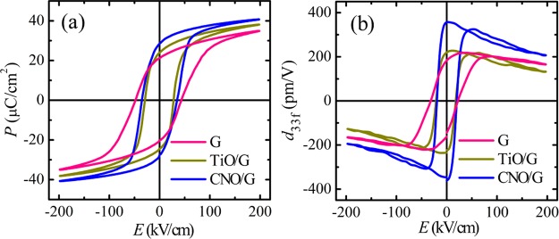
Figure 8 compares the polarization and piezoelectric properties of PZT films deposited on LNO buffered glass, TiOns/glass, and CNOns/glass at 50 Hz and 600 °C. The d33f value of PZT film on TiOns/glass (215 pm V–1) is also much lower than that on CNOns/glass (356 pm V–1). It indicates that not only the columnar structure but also the film orientation affect the piezoelectric coefficient. In this case, when an external electric field is applied along the [001] direction, i.e., perpendicular to the film surface, a large strain is achieved due to extensive non-180° domain switching,37 and therefore a higher d33f value is obtained in the (001)-oriented PZT film. The (001)-oriented PZT film has also a larger remanent polarization because the spontaneous polarization is along the [001] crystallographic direction, as shown in Figure 8a and Table 1. Moreover, the low void fraction and thus the strong effect of clamping is also a reason in the low d33f value in PZT film on TiOns/glass.
Figure 8.
(a) P–E and (b) small-signal d33f–E hysteresis loops, of 2-μm-thick PZT films deposited (at 50 Hz and 600 °C) on LNO buffered glass, TiOns/glass, and CNOns/glass.
Effect of Substrate Types
To investigate the effect of substrates on the piezoelectric properties, the 2-μm-thick PZT films with (001) orientation are deposited at 50 Hz and 600 °C on LNO/CNOns/glass, LNO/CNOns/Si, and LNO/SrTiO3 (STO(001)) substrates. The expected (001) orientation with minor (110) orientation is observed in the PZT films on CNOns/glass and CNOns/Si, while the film on STO is only (001) oriented, as shown in Figure 9. The fwhm value of the PZT(002) rocking curve in the film on CNOns/Si is approximately equal to that of the film on CNOns/glass, while a smaller fwhm value is obtained for the film on STO due to good lattice match and highly in-plane orientation (Table 1).
Figure 9.
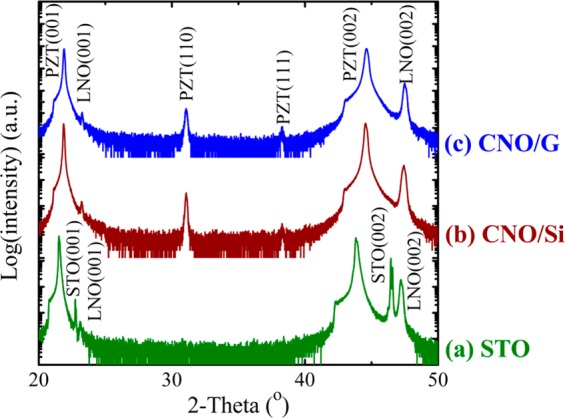
XRD θ–2θ patterns of 2-μm-thick PZT films deposited (at 50 Hz and 600 °C) on LNO buffered (a) SrTiO3 (STO, 001), (b) CNOns/Si, and (c) CNOns/glass.
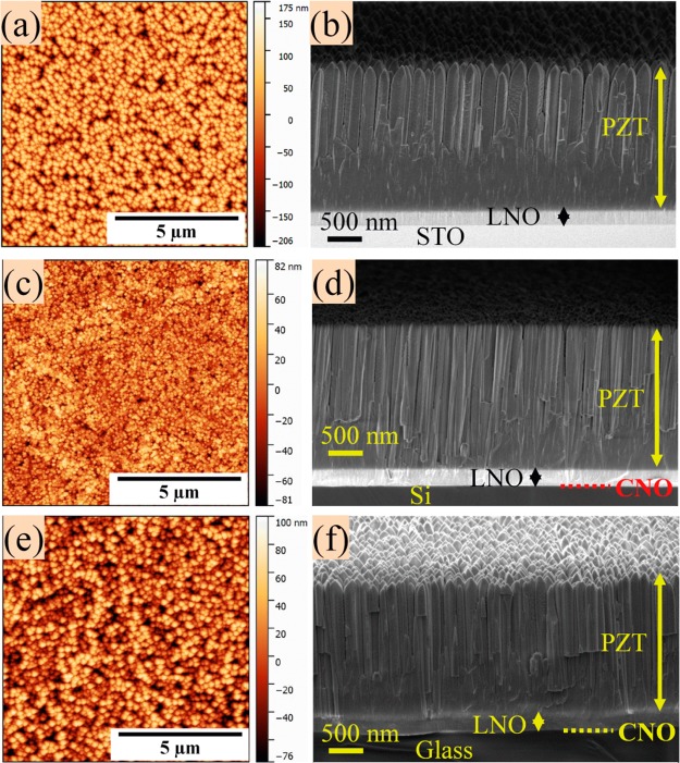
The columnar growth in these films is illustrated in Figure 10, in which the columnar-grain sizes are about 174, 110, and 192 nm, respectively, for the films on CNOns/glass, CNOns/Si, and STO. It is interesting to note that the columnar growth is also obtained in the film on single-crystal STO substrate at high laser frequency (50 Hz) although the average columnar grain size is much larger than in the films on CNOns/glass and CNOns/Si. Also the surface of the film on STO becomes much rougher, reflecting the larger dcol. More details on the grain size and surface roughness are given in Table 1.
Figure 10.
AFM and cross-sectional SEM images of 2-μm-thick PZT films deposited (at 50 Hz and 600 °C) on LNO buffered (a,b) STO, (c,d) CNOns/Si, and (e,f) CNOns/glass.
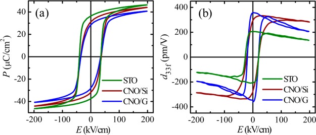
The P–E loops in Figure 11a for the films grown on CNOns/glass and CNOns/Si are very much comparable (although the CNOns/Si device has a slightly larger polarization), but a much higher polarization is observed in the film on STO. We attribute this to the difference in thermal expansion coefficients (TEC) of the substrates, inducing less in-plane tensile strain in PZT on CNOns/Si than that on CNOns/glass, while there is the in-plane compressive strain in PZT on STO, causing increasing polarization out of the film plane (TEC of PZT is 6.0 ppm K–1,38−40 Si ≈ 4.4 ppm K–1,41 ULE glass ≈ 0 ppm K–1,42 and STO ≈ 11.0 ppm K–1.43).
Figure 11.
(a) P–E and (b) small-signal d33f–E hysteresis loops, of 2-μm-thick PZT films deposited (at 50 Hz and 600 °C) on LNO buffered STO, CNOns/Si, and CNOns/glass substrates.
Figure 11b shows the piezoelectric d33f–E loops of PZT/LNO films on CNOns/glass, CNOns/Si, and STO substrates. It was found that the larger d33f value of the PZT film on CNOns/glass than those on CNOns/Si and STO. For these relatively thin films a large fraction of the clamping is due to the substrate, that is expected to be proportional to the Young’s modulus (Ys) of the substrate (Ys = 238 GPa for STO substrate,44 which is much higher than that of Si (Ys = 150 GPa)45 and glass (Ys = 67.6 GPa)42 substrates). Thus, one may expect with decreasing Ys the effective piezoelectric coefficient of the film increases, as is observed.
In the above, we have interpreted the trends in the piezoelectric coefficient (and polarization) in terms of changes in the clamping of the grains in the different films. We have assumed that this clamping decreases with increasing (average) grain separation and decreasing stiffness of the substrate. In Figure 12, the d33f value is plotted versus the ratio δ/Ys, where δ is the estimated spacing between the grains in the phyllo and Ys is the Young’s modulus of the substrate.46 The graph shows a clear positive correlation between δ/Ys and d33f, which holds for these 2-μm-thick PZT films grown on nanosheets buffered different substrates and deposited at different temperatures at 50 Hz deposition frequency, thus with (predominantly) highly oriented growth. The dependence of d33f of films deposited with varying pulse rate is much weaker but shows the same trend. A clear exception is the film grown directly on glass, which is polycrystalline with different growth orientations. No correlation was found between grain diameter and d33f (see Figure S5). These results support the assumption that clamping between grains and with the substrate determines to a large extent the extrinsic contribution to the piezoelectric coefficient.
Figure 12.
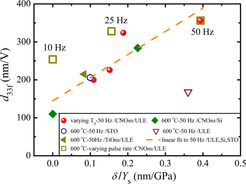
Effective piezoelectric coefficient as a function of the ratio of the grain spacing (δ) in the film and the Young’s modulus (Ys) of the substrate.
Conclusions
In summary, 2-μm-thick (001)-oriented PZT films with large piezoelectric coefficients were fabricated on glass using CNOns as a seed layer. Films with highly vertically aligned, largely separated columns resulted from using a laser frequency of 50 Hz. Well-developed polarization and piezoelectric hysteresis loops were obtained down to temperatures as low as 450 °C and represents an important advantage for the integration with CMOS devices. The enhanced piezoelectricity of these PZT films was explained in terms of the columnar microstructure that allows for a reduced clamping of the film. The small differences with films grown on ns-buffered Si and STO substrates were attributed to differences in thermal expansion coefficients of the substrates. These films on glass (and Si) with very high piezoelectric coefficient may be used in a wide range of applications, including adjustable X-ray or EUV optics.
Acknowledgments
This research was supported by the project number M62.3.10404 in the framework of the Research Program of the Materials innovation institute (M2i) (www.m2i.nl) and by the NanoNextNL—a micro and nanotechnology consortium of the Government of The Netherlands and 130 partners. The authors thank Mr. Mark Smithers for performing the HRSEM experiment and Dr. Rico Keim for the TEM measurement.
Supporting Information Available
The Supporting Information is available free of charge on the ACS Publications website at DOI: 10.1021/acsami.7b07428.
AFM images of a monolayer Ca2Nb3O10 (CNOns) nanosheet deposited on glass and Si, and Ti0.87O2 (TiOns) on glass by the Langmuir–Blodgett (LB) method; Flow diagram for etching process of Pb(Zr0.52Ti0.48)O3 (PZT) film capacitors; X-ray rocking curves of PZT films grown on LNO/CNOns/glass substrates: varying deposition temperature and at 50 Hz laser frequency, and varying laser frequency and with deposition temperature of 600 °C; Piezoelectric large-signal butterfly shaped bipolar strain-field (S–E) curves and unipolar strain-field (S–E) loops of the PZT films deposited on CNOns/glass at different repetition frequencies; Measured piezoelectric coefficient (d33f) for the PZT films deposited on CNOns/glass at different repetition frequencies; Piezoelectric coefficient versus grain diameter; Piezoelectric coefficient (d33f) as a function of the number of working cycles for PZT films on CNOns/glass, TiOns/glass, CNOns/Si, and STO (PDF)
Author Contributions
M.D.N. and G.R. conceived and designed the experiments. M.D.N. deposited the piezoelectric films; designed and fabricated the device structures; and performed and analyzed the microstructure, ferroelectric, and piezoelectric characterizations. H.Y. made the nanosheets under the supervision of J.E.E. B.J.W.E. measured the deflection of piezoelectric film capacitor by white-light interferometer. M.D.N., E.P.H., and G.R. wrote the paper with the help of the other authors. All authors discussed the results, commented on the manuscript, and gave their approval to the final version of the manuscript.
The authors declare no competing financial interest.
Supplementary Material
References
- Fu D.; Suzuki K.; Kato K.; Suzuki H. Dynamics of Nanoscale Polarization Backswitching in Tetragonal Lead Zirconate Titanate Thin Film. Appl. Phys. Lett. 2003, 82, 2130–2132. 10.1063/1.1565502. [DOI] [Google Scholar]
- Yamakawa K.; Imai K.; Arisumi O.; Arikado T.; Yoshioka M.; Owada T.; Okumura K. Novel Pb(Ti,Zr)O3 (PZT) Crystallization Technique Using Flash Lamp for Ferroelectric RAM (FeRAM) Embedded LSIs and One Transistor Type FeRAM Devices. Jpn. J. Appl. Phys. 2002, 41, 2630–2634. 10.1143/JJAP.41.2630. [DOI] [Google Scholar]
- Yang E. H.; Hishinuma Y.; Cheng J. G.; Trolier-Mckinstry S.; Bloemhof E.; Levine B. M. Thin-Film Piezoelectric Unimorph Actuator-Based Deformable Mirror with a Transferred Silicon Membrane. J. Microelectromech. Syst. 2006, 15, 1214–1225. 10.1109/JMEMS.2006.880208. [DOI] [Google Scholar]
- Nguyen M. D.; Yuan H.; Houwman E. P.; Dekkers M.; Koster G.; ten Elshof J. E.; Rijnders G. Highly Oriented Growth of Piezoelectric Thin Films on Silicon Using Two-Dimensional Nanosheets as Growth Template Layer. ACS Appl. Mater. Interfaces 2016, 8, 31120–31127. 10.1021/acsami.6b09470. [DOI] [PubMed] [Google Scholar]
- Cheng T. D.; Zhou N. J.; Li P. Ferroelectric and Photoelectricity Properties of (Pb0.52Zr0.48)TiO3 Thin Films Fabricated on FTO Glass Substrate. J. Mater. Sci.: Mater. Electron. 2015, 26, 7104–7108. 10.1007/s10854-015-3332-5. [DOI] [Google Scholar]
- Davies R. Telescopes of the Future. Astron. Geophys. 2012, 53, 15–18. 10.1111/j.1468-4004.2012.53415.x. [DOI] [Google Scholar]
- Favero I.; Karrai K. Optomechanics of Deformable Optical Cavities. Nat. Photonics 2009, 3, 201–205. 10.1038/nphoton.2009.42. [DOI] [Google Scholar]
- Savage N. Adaptive Optics. Nat. Photonics 2008, 2, 756–757. 10.1038/nphoton.2008.245. [DOI] [Google Scholar]
- Bayraktar M.; Chopra A.; Rijnders G.; Boller K.; Bijkerk F. Wavefront Correction in the Extreme Ultraviolet Wavelength Range using Piezoelectric Thin Films. Opt. Express 2014, 22, 30623–30632. 10.1364/OE.22.030623. [DOI] [PubMed] [Google Scholar]
- Choi J.-J.; Park G.-T.; Kim H.-E. Electrooptic Properties of Highly Oriented Pb(Zr,Ti)O3 Film Grown on Glass Substrate using Lanthanum Nitrate as a Buffer Layer. J. Mater. Res. 2004, 19, 3152–3156. 10.1557/JMR.2004.0432. [DOI] [Google Scholar]
- Kikuta K.; Noda K.; Okumura S.; Yamaguchi T.; Hirano S. Orientation Control of Perovskite Thin Films on Glass Substrates by the Application of a Seed Layer Prepared from Oxide Nanosheets. J. Sol-Gel Sci. Technol. 2007, 42, 381–387. 10.1007/s10971-006-0200-z. [DOI] [Google Scholar]
- Bayraktar M.; Chopra A.; Bijkerk F.; Rijnders G. Nanosheet Controlled Epitaxial Growth of PbZr0.52Ti0.48O3 Thin Films on Glass Substrates. Appl. Phys. Lett. 2014, 105, 132904. 10.1063/1.4896991. [DOI] [Google Scholar]
- Jaffe B.; Cook W. R. Jr.; Jaffe H.. Piezoelectric Ceramics; Academic Press Inc.: London, 1971. [Google Scholar]
- Trolier-McKinstry S.; Muralt P. Thin Film Piezoelectrics for MEMS. J. Electroceram. 2004, 12, 7–17. 10.1023/B:JECR.0000033998.72845.51. [DOI] [Google Scholar]
- Horwitz J. S.; Grabowski K. S.; Chrisey D. B.; Leuchtner R. E. Insitu Deposition of Epitaxial PbZrxTi(1–x)O3 Thin Films by Pulsed Laser Deposition. Appl. Phys. Lett. 1991, 59, 1565–1567. 10.1063/1.106284. [DOI] [Google Scholar]
- Galca A. C.; Stancu V.; Husanu M. A.; Dragoi C.; Gheorghe N. G.; Trupina L.; Enculescu M.; Vasile E. Substrate–Target Distance Dependence of Structural and Optical Properties in Case of Pb(Zr,Ti)O3 Films Obtained by Pulsed Laser Deposition. Appl. Surf. Sci. 2011, 257, 5938–5943. 10.1016/j.apsusc.2011.01.056. [DOI] [Google Scholar]
- Guan L.; Zhang D. M.; Li X.; Li Z. H. Role of Pulse Repetition Rate in Film Growth of Pulsed Laser Deposition. Nucl. Instrum. Methods Phys. Res., Sect. B 2008, 266, 57–62. 10.1016/j.nimb.2007.10.011. [DOI] [Google Scholar]
- Tyunina M.; Leppävuori S. Effects of Laser Fluence, Size, and Shape of the Laser Focal Spot in Pulsed Laser Deposition using a Multielemental Target. J. Appl. Phys. 2000, 87, 8132–8142. 10.1063/1.373508. [DOI] [Google Scholar]
- Zhu T. J.; Lu L.; Lai M. O. Pulsed Laser Deposition of Lead-Zirconate-Titanate Thin Films and Multilayered Heterostructures. Appl. Phys. A: Mater. Sci. Process. 2005, 81, 701–714. 10.1007/s00339-005-3227-z. [DOI] [Google Scholar]
- Blank D. H. A.; Dekkers M.; Rijnders G. Pulsed Laser Deposition in Twente: from Research Tool towards Industrial Deposition. J. Phys. D: Appl. Phys. 2014, 47, 034006. 10.1088/0022-3727/47/3/034006. [DOI] [Google Scholar]
- Leufke P. M.; Kruk R.; Wang D.; Kübel C.; Hahn H. Ferroelectric vs. Structural Properties of Large-Distance Sputtered Epitaxial LSMO/PZT Heterostructures. AIP Adv. 2012, 2, 032184. 10.1063/1.4756997. [DOI] [Google Scholar]
- Jacobsen H.; Prume K.; Wagner B.; Ortner K.; Jung T. High-Rate Sputtering of Thick PZT Thin Films for MEMS. J. Electroceram. 2010, 25, 198–202. 10.1007/s10832-010-9615-6. [DOI] [Google Scholar]
- Berfield T. A.; Ong R. J.; Payne D. A.; Sottos N. R. Residual Stress Effects on Piezoelectric Response of Sol-Gel Derived Lead Zirconate Titanate Thin Films. J. Appl. Phys. 2007, 101, 024102. 10.1063/1.2422778. [DOI] [Google Scholar]
- Wang G. S.; Rémiens D.; Soyer C. Combined Annealing Temperature and Thickness Effects on Properties of PbZr0.53Ti0.47O3 Films on LaNiO3/Si Substrate by Sol–Gel Process. J. Cryst. Growth 2006, 293, 370–375. 10.1016/j.jcrysgro.2006.06.014. [DOI] [Google Scholar]
- Dale D.; Fleet A.; Suzuki Y.; Brock J. D. X-ray Scattering from Real Surfaces: Discrete and Continuous Components of Roughness. Phys. Rev. B: Condens. Matter Mater. Phys. 2006, 74, 085419. 10.1103/PhysRevB.74.085419. [DOI] [Google Scholar]
- Nijland M.; Kumar S.; Lubbers R.; Blank D. H. A.; Rijnders G.; Koster G.; ten Elshof J. E. Local Control over Nucleation of Epitaxial Thin Films by Seed Layers of Inorganic Nanosheets. ACS Appl. Mater. Interfaces 2014, 6, 2777–2785. 10.1021/am4052624. [DOI] [PubMed] [Google Scholar]
- Shibata T.; Takano H.; Ebina Y.; Kim D. S.; Ozawa T. C.; Akatsuka K.; Ohnishi T.; Takada K.; Kogure T.; Sasaki T. Versatile van der Waals Epitaxy-Like Growth of Crystal Films using Two-Dimensional Nanosheets as a Seed Layer: Orientation Tuning of SrTiO3 Films along Three Important Axes on Glass Substrates. J. Mater. Chem. C 2014, 2, 441–449. 10.1039/C3TC31787K. [DOI] [Google Scholar]
- Yuan H.; Lubbers R.; Besselink R.; Nijland M.; ten Elshof J. E. Improved Langmuir–Blodgett Titanate Films via in Situ Exfoliation Study and Optimization of Deposition Parameters. ACS Appl. Mater. Interfaces 2014, 6, 8567–8574. 10.1021/am501380d. [DOI] [PubMed] [Google Scholar]
- Yuan H.; Nguyen M.; Hammer T.; Koster G.; Rijnders G.; ten Elshof J. E. Synthesis of KCa2Nb3O10 Crystals with Varying Grain Sizes and Their Nanosheet Monolayer Films as Seed Layers for PiezoMEMS Applications. ACS Appl. Mater. Interfaces 2015, 7, 27473–27478. 10.1021/acsami.5b09456. [DOI] [PubMed] [Google Scholar]
- Pham M. T. N.; Boukamp B. A.; Rijnders G.; Bouwmeester H. J. M.; Blank D. H. A. Pulsed Laser Deposition of PZT/Pt Composite Thin Films with High Dielectric Constants. Appl. Phys. A: Mater. Sci. Process. 2004, 79, 907–910. 10.1007/s00339-004-2822-8. [DOI] [Google Scholar]
- Ramesh R.; Inam A.; Chan W. K.; Tillerot F.; Wilkens B.; Chang C. C.; Sands T.; Tarascon J. M.; Keramidas V. G. Ferroelectric PbZr0.2Ti0.8O3 Thin Films on Epitaxial Y-Ba-Cu-O. Appl. Phys. Lett. 1991, 59, 3542–3544. 10.1063/1.105651. [DOI] [Google Scholar]
- Nguyen M. D.; Houwman E. P.; Dekkers M.; Rijnders G. Strongly Enhanced Piezoelectric Response in Lead Zirconate Titanate Films with Vertically Aligned Columnar Grains. ACS Appl. Mater. Interfaces 2017, 9, 9849–9861. 10.1021/acsami.6b16470. [DOI] [PMC free article] [PubMed] [Google Scholar]
- Haun M. J.; Furman E.; Jang S. J.; Cross L. E. Thermodynamic Theory of the Lead Zirconate-Titanate Solid Solution System, Part V: Theoretical Calculations. Ferroelectrics 1989, 99, 63–86. 10.1080/00150198908221440. [DOI] [Google Scholar]
- Cao Y.; Sheng G.; Zhang J. X.; Choudhury S.; Li Y. L.; Randall C. A.; Chen L. Q. Piezoelectric Response of Single-Crystal PbZr1–xTixO3 near Morphotropic Phase Boundary Predicted by Phase-Field Simulation. Appl. Phys. Lett. 2010, 97, 252904. 10.1063/1.3530443. [DOI] [Google Scholar]
- Yao F. Z.; Yu Q.; Wang K.; Li Q.; Li J. F. Ferroelectric Domain Morphology and Temperature-Dependent Piezoelectricity of (K,Na,Li)(Nb,Ta,Sb)O3 Lead-Free Piezoceramics. RSC Adv. 2014, 4, 20062–20068. 10.1039/C4RA01697A. [DOI] [Google Scholar]
- Tang H.; Zhang S.; Feng Y.; Li F.; Shrout T. R. Piezoelectric Property and Strain Behavior of Pb(Yb0.5Nb0.5)O3–PbHfO3–PbTiO3 Polycrystalline Ceramics. J. Am. Ceram. Soc. 2013, 96, 2857–2863. 10.1111/jace.12389. [DOI] [Google Scholar]
- Zhang J. X.; Sheng G.; Chen L. Q. Large Electric Field Induced Strains in Ferroelectric Islands. Appl. Phys. Lett. 2010, 96, 132901. 10.1063/1.3373915. [DOI] [Google Scholar]
- Wang J.; Zheng H.; Ma Z.; Prasertchoung S.; Wuttig M.; Droopad R.; Yu J.; Eisenbeiser K.; Ramesh R. Epitaxial BiFeO3 Thin Films on Si. Appl. Phys. Lett. 2004, 85, 2574–2576. 10.1063/1.1799234. [DOI] [Google Scholar]
- Yang S. Y.; Zavaliche F.; Mohaddes-Ardabili L.; Vaithyanathan V.; Schlom D. G.; Lee Y. J.; Chu Y. H.; Cruz M. P.; Zhan Q.; Zhao T.; Ramesh R. Metalorganic Chemical Vapor Deposition of Lead-Free Ferroelectric BiFeO3 Films for Memory Applications. Appl. Phys. Lett. 2005, 87, 102903. 10.1063/1.2041830. [DOI] [Google Scholar]
- Kurihara K.; Kondo M.; Sato K.; Ishii M.; Wakiya N.; Shinozaki K. Electrooptic Properties of Epitaxial Lead Zirconate Titanate Films on Silicon Substrates. Jpn. J. Appl. Phys. 2007, 46, 6929–6932. 10.1143/JJAP.46.6929. [DOI] [Google Scholar]
- Wang G. S.; Rémiens D.; Dogheche E.; Dong X. L. Effect of Thermal Strain on Structure and Polarization Fatigue of CSD-Derived PbZr0.53Ti0.47O3/LaNiO3 hetero-Structures. Appl. Phys. A: Mater. Sci. Process. 2007, 88, 657–660. 10.1007/s00339-007-4022-9. [DOI] [Google Scholar]
- http://www.sydor.com/wp-content/uploads/Corning-ULE-7972-Low-Expansion-Glass.pdf.
- Kawashima J.; Yamada Y.; Hirabayashi I. Critical Thickness and Effective Thermal Expansion Coefficient of YBCO Crystalline Film. Phys. C 1998, 306, 114–118. 10.1016/S0921-4534(98)00350-5. [DOI] [Google Scholar]
- Paufler P.; Bergk B.; Reibold M.; Belger A.; Pätzke N.; Meyer D. C. Why is SrTiO3 Much Stronger at Nanometer than at Centimeter Scale?. Solid State Sci. 2006, 8, 782–792. 10.1016/j.solidstatesciences.2006.04.005. [DOI] [Google Scholar]
- Lee J.-W.; Choi J.-J.; Park G.-T.; Park C.-S.; Kim H.-E. Thick Pb(Zr,Ti)O3 Films Fabricated by Inducing Residual Compressive Stress during the Annealing Process. J. Mater. Res. 2005, 20, 2898–2901. 10.1557/JMR.2005.0383. [DOI] [Google Scholar]
- A more detailed model of the clamping may provide a more accurate relation between d33f, grain separation, and the effect of substrate clamping. One expects that for increasing film thickness, the effect of substrate clamping is relatively smaller compared to the effect of the grain separation. This is indeed observed ref (32). Here the film thickness is constant. The strong effect of the pulse rate suggests that the relative effect of substrate induced clamping compared to grain-to-grain clamping becomes larger for higher pulse rate, resulting in denser films (lower void fraction) in combination with larger diameter grains. This appears to be have assumed the most simple linear dependence.
Associated Data
This section collects any data citations, data availability statements, or supplementary materials included in this article.


