Abstract
Highly ordered TiO2 nanotube (TNT) arrays were successfully synthesized by the combination of soft and hard templates. In the fabrication of them, anodic aluminum oxide membranes act as the hard template while the self-assembly of polystyrene-block-poly(ethylene oxide) (PS-b-PEO) complexed with titanium-tetraisopropoxide (TTIP, the precursor of TiO2) provides the soft template to control the grain size of TiO2 nanotubes. Our results indicate that the field emission (FE) performance depends crucially on the grain size of the calcinated TiO2 which is dominated by the PS-b-PEO and its blending ratio with TTIP. The optimized sample (with the TTIP/PEO ratio of 3.87) exhibits excellent FE performances involving both a low turn-on field of 3.3 V/um and a high current density of 7.6 mA/cm2 at 12.7 V/μm. The enhanced FE properties can be attributed to the low effective work function (1.2 eV) resulted from the smaller grain size of TiO2.
Keywords: Nanocrystalline materials, Polymers, Surfaces, Microstructure
Background
One-dimensional nanomaterials have attracted great interest due to their potential for numerous applications, e.g., electron field emitter [1–5]. TiO2 nanotubes (TNTs) are promising candidate for the emitter due to the high aspect ratio, low work function (4.5 eV), and high oxidation resistance [4]. The nanotube diameters, height, wall thickness, and density as well as the regularity of the nanoarray dependences of the field emission (FE) performance have been investigated in detail [6, 7]. A significant number of nanotube arrays are available by the aid of the development of the synthetic approaches [8, 9]. Especially, the template strategies have been widely employed to fabricate nanotube array. For instance, Tsai et al. prepared diamond nanotip arrays with various sizes and periods by anodic aluminum oxide (AAO) [10]. During the preparation, the micro-channels in AAO membrane can act as an excellent hard template to induce the formation of highly ordered nanoarrays. In the synthesis of porous TiO2 nanofibers in our previous work, the self-assembly of block copolymer has been proved as an effective template for the selective distribution and the grain size manipulation of TiO2 [11]. The highly ordered TNT arrays with tunable grain sizes can be expected by the combination of the soft and hard templates. For one thing, it is facile to tailor the diameter, center-to-center distance, and the length of the TiO2 arrays by means of various AAO membranes; for another thing, the wall thickness, grain size, and the density of the TiO2 nanotubes are under the control of the block copolymer and the precursor of TiO2. Most importantly, the structure control in TNT array and tube levels can be performed separately. In this work, therefore, the TiO2 arrays with various grain sizes have been fabricated in the blend of titanium-tetraisopropoxide (TTIP)/block copolymer. In addition to the hard template (AAO) for the formation of highly ordered arrays, the PS-b-PEO is employed as the soft template to control the grain size of TiO2. The field emission performances of the resultant TNT arrays exhibit obvious grain size dependence, which has been attributed to the variation of the effective work function.
Methods
The porous AAO membrane (Whatman, Germany) with the pore size of ~ 200 nm and the thickness of 60 μm and polystyrene-block-poly(ethylene oxide) (Sigma-Aldrich, USA) with a molecular weight of 58,500–37,000, 58,600–71,000, and 60000–14,500 g/mol were used. Titanium-tetraisopropoxide (TTIP, Sigma-Aldrich, USA) acts as the precursor of TiO2. PS-b-PEO and TTIP were dissolved in chloroform with various composition ratios (Table 1). S1 to S5 are samples corresponding to the indicated block copolymer and the blend ratio. For instance, S1 was prepared using the block copolymer of Mw = 58,500–37,000 and the TTIP/PEO blend ratio of 3.87. After stirring for 5 h at room temperature, the mixed solution was transferred to the bottom of AAO membranes. The solution can go into the channels in AAO upon the capillary effect. Then, the samples were dried at 120 °C for 12 h in vacuum. After calcined at 450 °C for 2 h in air, the samples were immersed in NaOH solution (3 mol/L) for 1 h to remove the alumina frame. Finally, the products were washed with deionized water and dried at 40 °C for 24 h (Scheme 1).
Table 1.
Samples with various molecular weights of PS-b-PEO and its blending ratio with TTIP
| Sample name | S1 | S2 | S3 | S4 | S5 |
|---|---|---|---|---|---|
| PS-PEO | 58,500–37,000 | 58,500–37,000 | 58,500–37,000 | 60,000–14,500 | 58,600–71,000 |
| TTIP/PEOa | 3.87 | 5.16 | 10.32 | 3.64 | 3.70 |
| Grain size (nm)b | 10.7 | 12.5 | 14.9 | 11.8 | 13.5 |
aTTIP/PEO represents the weight ratio between TTIP and PEO in PS-b-PEO
bGrain sizes were calculated from XRD profiles shown in Fig. 2
Scheme 1.

Preparation of TNT arrays with the combination of soft and hard templates
A Hitachi S-4800 FESEM was used for morphology measurement at an accelerating voltage of 5.0 kV. The X-ray diffraction (smartlab3, Rigaku Japan) data were collected at a scanning speed of 2°/min with a step interval of 0.02°. The electron field emission measurements were carried out using a diode configuration, a cathode (sample), and a parallel anode plate at a distance of 150 μm in a vacuum chamber (2 × 10⁻⁶ Torr).
Results and Discussion
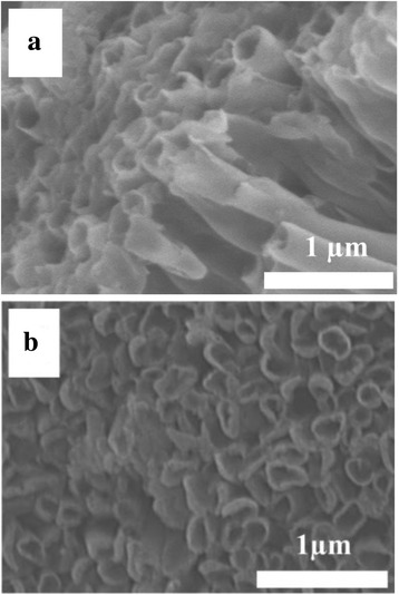
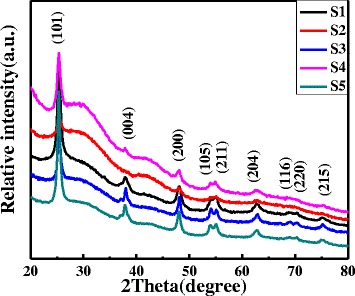
Figure 1 shows the typical SEM images of TNT arrays by taking S1 as an example (all samples exhibit similar morphologies). In the SEM image of the side view (Fig. 1a), there are some vertically aligned nanotubes with the diameter of ~ 200 nm. Figure 1b illustrates the SEM images of the top view of TNT arrays, in which the diameter of the nanotubes can be further confirmed. Figure 2 shows the XRD profiles of all samples dried at 40 °C for 24 h. There are strong diffraction peaks locating at 25°, 38°, and 48°, which agrees well with the reported values of anatase TiO2 from JCPDS Card No. 84-1286. All samples exhibit strong preferential growth orientations along the (101) plane (25°). The mean grain sizes were calculated from the full width at half maximum (FWHM) of the (101) diffraction peaks using the Debye–Scherrer formula [12]:
where D, λ, β 2θ, and θ are the mean grain size, X-ray wavelength (1.5418 Å), FWHM in radians, and Bragg’s diffraction angle, respectively. The sample grain sizes are listed in Table 1. Obviously, the increase of TTIP weight fraction in the blend (from S1 to S3) results in the higher magnitude of grain size.
Fig. 1.

SEM images of obtained TNTs from the side (a) and top (b) view
Fig. 2.

XRD profiles of TNT arrays
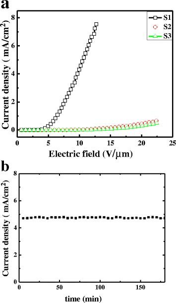
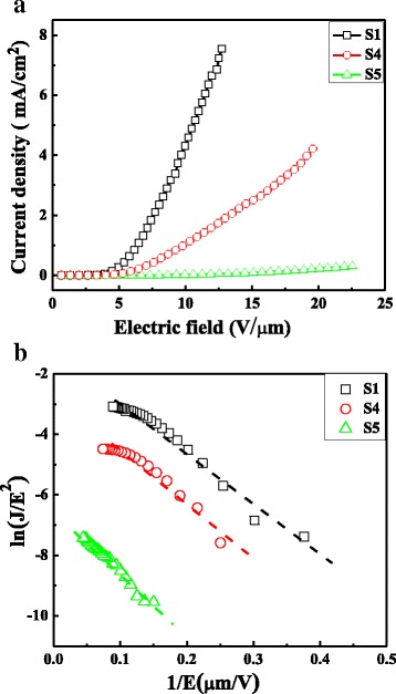
Fowler–Nordheim (F–N) theory is usually used to further analyze the FE properties of the TNT arrays [13]. It can be expressed as J = (Aβ 2 E 2/φ) exp(−Bφ 3/2/βE), where J is the FE current density (A/cm2), E is the applied electric field (V/μm), ∅ is the work function (4.5 eV for TiO2), β is the field enhancement factor related to the emitter geometry, and A and B are constants whose values are 1.56 × 10⁻⁶(A eV V−2) and 6.83 × 10³(eV−3/2 V μm−1), respectively. Figure 3a illustrates the current density–electric field (J–E) plot of TNT cathodes, which exhibit exponential dependence. The turn-on field and the threshold field are defined as the electric field at an emission current density of 0.01 and 1.0 mA/cm2, respectively. For S1, the turn-on field and threshold field are 3.3 and 6.4 V/μm, respectively, with excellent cycle stability as shown in Fig. 3b. However, the turn-on fields are 10.3 and 13.2 V/μm for S2 and S3, respectively. No threshold voltage is observed in the results of S2 and S3 within the studied electric field range. To clarify the reason for the great difference of field emission performance among them, our attention is paid to the different nanotube thicknesses and grain sizes of TiO2 obtained in XRD profiles. For one thing, the thicknesses (estimated in SEM images, data not shown here) are 24, 29, and 36 nm in S1, S2, and S3, respectively. For another thing, the grain sizes of anatase TiO2 obtained from XRD profiles are 10.7 (S1), 12.5 (S2), and 14.9 nm (S3) as shown in Table 1. To distinguish the roles of tube thickness and grain size in the field emission performance, the nanotubes with the similar thickness were prepared based on the blend ratios shown in Table 1. Figure 4a represents the field emission characteristic of these samples under an applied bias voltage. The average turn-on fields (obtained from at least three samples) of S1, S4, and S5 are 3.3 ± 0.4, 4.2 ± 0.3, and 8.7 ± 0.5 V/μm, respectively. Although there are kinds of parameters influencing field emission performance, it is still reasonable to attribute the different field emission performances to the grain size since the samples exhibiting the similar tube thickness were fabricated according to the same condition. Furthermore, the smaller size (10.7 nm for S1) corresponds to the lower turn-on field (3.3 V/μm). It is worth to notice that S1 exhibits the maximum current density as large as 7.6 mA/cm2 at the field of 12.7 V/μm which is much higher than the reported values while the turn-on field is comparable with the results in references [14–18].
Fig. 3.

Current density–electric field (J–E) plot (a) and the current density stability of S1 under 10 V μm−1 for 180 min (b)
Fig. 4.

a Current density–electric field (J–E) plot. b The corresponding Fowler–Nordheim plots
The FE behavior of TNTs can be modeled following the well-known Fowler–Nordheim (FN) equation, as shown in Fig. 4b. The good linear fit in the curves indicates that the field emission current originates only from barrier tunneling electrons extracted by the electric field. Based on the slope of the FN plot (k), it is facile to calculate the effective work functions using the following equation:
k = − (6.83 × 10³)φ 3/2/β.
They are 1.2, 1.5, and 2.1 eV for S1, S4, and S5, respectively, by assuming the field enhancement factor (pristine TNT arrays) is 445 [18]. The reduction in the turn-on electric field of the TNTs is caused by the decrease of the effective potential barrier height resulted from the smaller TiO2 grains. Therefore, it is reasonable to attribute the enhanced field performance to the grain boundary effect and resultant up-shift of Fermi level which can be interpreted as follows [4, 19]. Polycrystalline materials are composed of small nanocrystalline grains separated by grain boundaries, which lead to a large number of grain boundary defects. These defects are benefit for both electron trapping and electron supply due to the effective conducting pathway. This is the reason for the increase of carrier concentration and subsequent up-shift of Fermi level [19]. This rising Fermi level can reduce the work function (Fig. 4b) and the effective potential barrier height of TNTs, corresponding to easy electron emission, accounting for the enhanced field emission performance.
Conclusions
The TNT arrays were synthesized by the combination of soft and hard templates. On one hand, the AAO membranes induce the vertically aligned nanotubes. On the other hand, both the block copolymer and its blend ratio with TTIP produce remarkable influence on the grain size of the TiO2. The relationship between the grain size and the FE performance has been clarified for the first time. Our results indicate that the decrease of grain size accounts for the stronger grain boundary conduction, leading to the lift of the Fermi level. This is the reason for the lower work function, the smaller effective potential barrier, and the resultant-enhanced FE performance.
Acknowledgements
This work was financially supported by the National Natural Science Foundation of China (21234007 and 61504035).
Authors’ Contributions
YXX and MP performed the experiments, analyzed the data, and drafted the manuscript. QH and ZJX participated in the sample preparation and characterization. WQ participated in the measurement of field emission performance. The whole project was under the direction of YJC and LYJ, who designed the experiments and revised the manuscript. All authors read and approved the final manuscript.
Competing Interests
The authors declare that they have no competing interests.
Publisher’s Note
Springer Nature remains neutral with regard to jurisdictional claims in published maps and institutional affiliations.
Contributor Information
Jichun You, Email: you@hznu.edu.cn.
Yongjin Li, Email: Yongjin-li@hznu.edu.cn.
References
- 1.Deheer WA, Chatelain A, Ugarte DA. Carbon nanotube field-emission electron source. Science. 1995;270:1179–1180. doi: 10.1126/science.270.5239.1179. [DOI] [Google Scholar]
- 2.Pan ZW, Lai HL, Au FC, Duan XF, Zhou WY, Shi WS, Wang N, Lee CS, Wong NB, Lee ST, Xie SS. Oriented silicon carbide nanowires: synthesis and field emission properties. Adv Mater. 2000;12:1186–1190. doi: 10.1002/1521-4095(200008)12:16<1186::AID-ADMA1186>3.0.CO;2-F. [DOI] [Google Scholar]
- 3.Miyauchi M, Toda Y, Kamiya T, Hosono H. Electron field emission from TiO2 nanotube arrays synthesized by hydrothermal reaction. Appl Phys Lett. 2006;89:043114. doi: 10.1063/1.2245202. [DOI] [Google Scholar]
- 4.Liu G, Li F, Wang DW, Tang DM, Liu C, Ma XL, GQ L, Cheng HM. Electron field emission of a nitrogen-doped TiO2 nanotube array. Nanotechnology. 2008;19:025606. doi: 10.1088/0957-4484/19/02/025606. [DOI] [PubMed] [Google Scholar]
- 5.Yang Y, Wang X, Sun C. Electron field emission and photoluminescence of anatase nanotube arrays. J Am Ceram Soc. 2008;91:4109. doi: 10.1111/j.1551-2916.2008.02776.x. [DOI] [Google Scholar]
- 6.Li Y, Sun Y, Yeow JT. Nanotube field electron emission: principles, development, and applications. Nanotechnology. 2015;26:242001. doi: 10.1088/0957-4484/26/24/242001. [DOI] [PubMed] [Google Scholar]
- 7.Alivov Y, Klopfer M, Molloi S. Effect of TiO2 nanotube parameters on field emission properties. Nanotechnology. 2010;21:505706. doi: 10.1088/0957-4484/21/50/505706. [DOI] [PubMed] [Google Scholar]
- 8.Cui L, Hui KN, Hui KS, Lee SK, Zhou W, Wan ZP, Thuc CNH. Facile microwave-assisted hydrothermal synthesis of TiO2 Nanotubes. Mater Lett. 2012;75:175–178. doi: 10.1016/j.matlet.2012.02.004. [DOI] [Google Scholar]
- 9.Su Y, Zhang X, Han S, Chen X, Lei L. F–B-codoping of anodized TiO2 nanotubesusing chemical vapor deposition. Electrochem Commun. 2007;9:2291–2298. doi: 10.1016/j.elecom.2007.06.038. [DOI] [Google Scholar]
- 10.Tsai HY, Tseng PT. Field emission characteristics of diamond nano-tip array fabricated by anodic aluminum oxide template with nano-conical holes. Appl Surf Sci. 2015;351:1004–1010. doi: 10.1016/j.apsusc.2015.06.035. [DOI] [Google Scholar]
- 11.You JC, Sheng WJ, Huang K, Hou C, Yue H, Hu B, Wang M, Wei D, Li Q, Zhao L, Dong W, Zhao Z, Li YJ. Novel cigarlike TiO2 nanofibers: fabrication, improved mechanical, and electrochemical performances. ACS Appl Mater Interfaces. 2013;5:2278–2282. doi: 10.1021/am4003099. [DOI] [PubMed] [Google Scholar]
- 12.Zhang Z, Bao C, Ma S, Zhang L, Hou S. Effects of deposition power and pressure on the crystallinity of Al-doped ZnO thin films at glass substrates by low temperature RF magnetron sputtering. J Aust Ceram Soc. 2012;48:214–222. [Google Scholar]
- 13.Fowler RH, Nordheim LW. Electron emission in intense electric fields. Proc R Soc. 1928;119:173–181. doi: 10.1098/rspa.1928.0091. [DOI] [Google Scholar]
- 14.Chen J, Wang L, Wang C, Li D, Li Y, Wang J, Zhou F. Electron field emission from the semimetallic TiO2 nanotube arrays. Vacuum. 2013;96:18–21. doi: 10.1016/j.vacuum.2013.03.003. [DOI] [Google Scholar]
- 15.Song Z, Zhou H, Tao P, Wang B, Mei J, Wang H. The synthesis of TiO2 nanoflowers and their application in electron field emission and self-powered ultraviolet photodetector. Mater Lett. 2016;180:179–183. doi: 10.1016/j.matlet.2016.05.178. [DOI] [Google Scholar]
- 16.Chavan P, Shende S, Joag D, More M. Photo-enhanced field emission study of TiO2 nanotubes array. Ultramicroscopy. 2011;111:415–420. doi: 10.1016/j.ultramic.2010.11.001. [DOI] [PubMed] [Google Scholar]
- 17.Li D, Chen J, Wang C, Zhu W, Zhang L, Yan L, Wang J, Zhou F. Aligned rutile TiO2 nanorods: facile synthesis and field emission. Superlattices Microst. 2013;59:187–195. doi: 10.1016/j.spmi.2013.04.010. [DOI] [Google Scholar]
- 18.Zhu WD, Wang CW, Chen JB, Li DS, Zhou F, Zhang HL. Enhanced field emission from hydrogenated TiO2 nanotube arrays. Nanotechnology. 2012;23:455204. doi: 10.1088/0957-4484/23/45/455204. [DOI] [PubMed] [Google Scholar]
- 19.Sommer N, Hüpkes J, Rau U. Field emission at grain boundaries modeling the conductivity in highly doped polycrystalline semiconductors. Phys Rev Appl. 2016;5:024009. doi: 10.1103/PhysRevApplied.5.024009. [DOI] [Google Scholar]


