Abstract
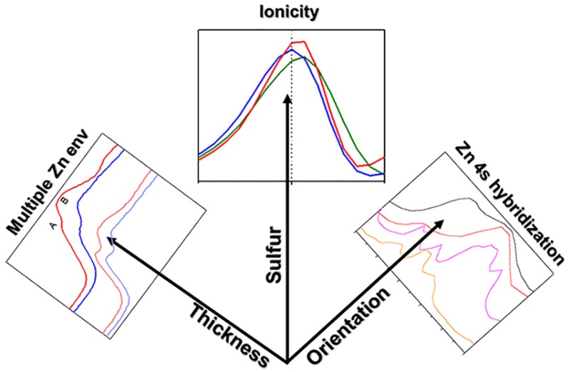
Zn(O,S) buffer layer electronic configuration is determined by its composition and thickness, tunable through atomic layer deposition. The Zn K and L-edges in the X-ray absorption near edge structure verify ionicity and covalency changes with S content. A high intensity shoulder in the Zn K-edge indicates strong Zn 4s hybridized states and a preferred c-axis orientation. 2–3 nm thick films with low S content show a subdued shoulder showing less contribution from Zn 4s hybridization. A lower energy shift with film thickness suggests a decreasing bandgap. Further, ZnSO4 forms at substrate interfaces, which may be detrimental for device performance.
Keywords: X-ray absorption near edge structure (XANES); Zn(O,S); atomic layer deposition (ALD); oxysulfide films; buffer layers
Zn(O,S) thin films are excellent alternatives for the commonplace toxic CdS layers in CIGSe solar cells.1,2 Atomic layer deposition (ALD) is an especially promising tool for Zn(O,S) fabrication, allowing precise tailoring of layer thickness and O/S ratio.3 The films’ key properties (band gap, conduction band offset, conductivity) can be changed, leading to higher overall efficiencies (18.5%4). Yet the standard technique, chemical bath deposition (CBD), still renders architectures with higher efficiencies. A better characterization of the structure–property relationships of ALD layers will further push their development and understanding.5 The elemental specificity of X-ray absorption techniques makes them promising for revealing atomic and electronic structure of ALD films.6−8 Via X-ray absorption near edge structure (XANES), the band gap bowing phenomenon with S concentrations was explained.9 The rise to S 3p–Zn 4sp–O 2p hybridized states with the incorporation of S in ZnO affects ionicities of certain bonds causing changes in the band gap. The interface of Zn(O,S) to ZnO electrodes contains sulfate due to S diffusion.10 Sulfate increases resistivity and loss in the fill factor, which may explain performance differences with different deposition methods.
These insights derived from studying the two ligands. The Zn metal edges can provide similar conclusions in addition to a deeper understanding of Zn coordination depending on compositions and thicknesses.
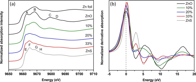
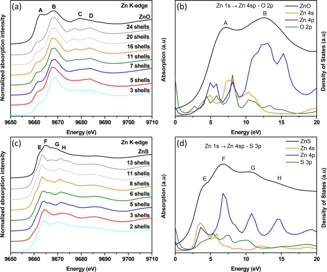
Figure 1a shows a comparison of XANES spectra at the Zn K-edge for Zn(O,S) films (50–60 nm) along with references (Zn(O,S) film details Figure S1). The ZnO reference has four features, A–D, ZnS reference with features E–H. ZnO appears similar to literature except for a stronger A peak.11−13 A and B show a transition from Zn 1s to Zn 4sp–O 2p and Zn 1s to Zn 4p–O 2p hybridized states of the conduction band respectively (Figure 2b). The stronger A peak is apparent in the ZnO and 10% samples (percentage is H2S to total oxidant (H2S+H2O) pulses, see Supporting Information). This indicates a preferred (200) orientation of ZnO unit cells (XRD Figure S2).9 The X-ray electric field interacts with the crystal in the (1,0,1) direction, the A/B ratio increases because of strong interaction with σ bonds.14,15
Figure 1.
(a) X-ray absorption characterization at Zn K-edge are shown for Zn(O,S) films deposited on Si substrates including references of Zn foil, ALD ZnO, and ZnS. Zn K-edge spectra were background subtracted and atomically normalized in the energy region from 9690 to 9700 eV. (b) Normalized derivative spectra of Zn K-edge.
Figure 2.
(a) Theoretical multiple scattering (MS) calculations at the Zn K-edge as a function of the cluster size for ZnO for clusters with increasing atomic shells: 3, 5, 7, 11, 16, 20, and 24. The 24-shell cluster corresponds to a sphere of radius 10 Å. The experimental ZnO curve is shown above as a reference. Feature D develops when 5 shells (short-range order) are considered and C appears when 11 shells (midrange order) are considered, predominantly pertaining to multiple scattering. (b) Calculations of the partial density of states (pDOS) of ZnO plotted together with the experimental XAS spectrum. The earlier part of conduction band is composed of hybridized O 2p–Zn 4sp states. (c) Theoretical MS calculations at the Zn K-edge as a function of the cluster size for ZnS for clusters with increasing atomic shells: 2, 3, 5, 6, 8, 11, and 13. The 13-shell cluster corresponds to a sphere of radius 10 Å. The experimental ZnS curve is shown above as a reference. Feature G and H develop when 5 shells (midrange order) are considered, predominantly pertaining to multiple scattering. (d) Calculations of the partial density of states (pDOS) of ZnS plotted together with the experimental XAS spectrum. The earlier part of conduction band is composed of hybridized S 3p–Zn 4sp states. Calculations of the partial density of states (pDOS) relative to the Fermi level (total density of states shifted so onset of band gap is at 0 eV) plotted together with the experimental XAS spectra [XAS spectrum aligned by matching max intensity to max pDOS intensity of absorbing atom] for b and d.
The free energy force field (FEFF) (feff is the effective curved wave scattering amplitude in the EXAFS equation) simulated curves match experimental references. ZnO appears a better match than ZnS, also observed previously.16 The pDOS calculations reveal that Zn 4p contributions are stronger for B. Lower energy Zn 4p and 4s contributions to A are lower, resulting in a lower A/B ratio in conventional ZnO films without preferred orientation (as the films observed here). C (midrange order) and D (short-range order) mainly arise from multiple scattering (Figure 2a). Features E and F are transitions from Zn 1s to Zn 4sp–S 3p and Zn 1s to Zn 4p–S 3p hybridized states of the conduction band respectively (Figure 2d). From Figure 2c, peaks G and H (midrange order) arise from multiple scattering with contributions from a transition to Zn 4p states (Figure 2d). 10% bears great resemblance to reference ZnO, with the least S but a noticeable change in the Zn environment within the largely ZnO matrix. B/A has decreased. The broadening indicates a distortion in the local bonding environment with S incorporation affecting the orbital mixing. The participation of O 2p orbitals likely forms Zn 4sp–S 3p–O 2p hybridized states. B has a low energy shift, indicating longer Zn–O bonds.17 C and D are weaker because of the disruption of long-range order with S atoms into the ZnO. 20% appears nearly featureless. Its spectral shape is a better match with the reference ZnS. This corroborates with the 20% XRD pattern shown previously (broad peak at 2θ above ZnS (111) and below ZnO (100)).9 The lack of features suggests Zn is present in several environments. F/E is almost unity because of this heterogeneity. E rises from newly formed hybridized states with O 2p orbitals as shown in previous DOS calculations for the ternary films. H is no longer present. The distortion resulted in a reduction of order corroborated by our previous findings.9 33% is similar to ZnS with a few differences. F/E is lower because of hybridized O 2p orbitals to E. G is weaker because of distortions caused by O. Modified hybridized states in the conduction band have more distinct resonances in the near edge with O 2p character changing the structure and the spectrum (summary of Zn K-edge XANES in Table 1). The intensity and full width at half-maximum (fwhm) of the first peak is a measure of the relative ionicity/covalency of the system.18,19 A clear trend is present in the intensity of the first peak (Figure 1b). With increasing S, it increases and broadens, resulting in a larger fwhm. The ionicity is increasing; the Zn–O bonds lengthen with S, as previously suggested.9 The shift of the first peak in the Zn K-edge (∼0.5 eV, Figure S3), and the spectral weight shift to lower energy seen in the Zn L-edge (Figure 3) corroborates this. Here, this is concluded from experimental results only, as the ionicity is apparent. For the O–K edge, this was concluded only after performing a series of multiple scattering (MS) simulations.
Table 1. Zn K-Edge Features and Qualitative Assignments for ZnO and ZnSa.
| label | energy (eV) | assignment |
|---|---|---|
| A | 9663.8 | Zn 1s → Zn 4sp – O 2p |
| B | 9668.4 | Zn 1s → Zn 4p – O 2p |
| C | 9679.3 | MS (11 shells midrange order) |
| D | 9683.4 | MS (5 shells short-range order) |
| E | 9662.8 | Zn 1s → Zn 4sp – S 3p |
| F | 9664.9 | Zn 1s → Zn 4p – S 3p |
| G and H | 9669.1 and 9672.6 | MS (5 shells midrange order) |
MS = multiple scattering and its assignment means it is a major contributor to that particular peak. Assignment of hybridized states means that it is a contributor of a peak along with short- and long-range orders.
Figure 3.
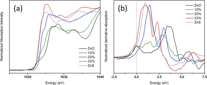
(a) X-ray absorption characterization at Zn LIII-edge is shown for Zn(O,S) films deposited on SiO2 including references of ALD ZnO and ZnS. Zn L-edge spectra were background subtracted and atomically normalized in the energy region from 1063–1073 eV. (b) Derivative absorption spectra at Zn LIII-edge showing that as the S concentration increases, so too does the ionicity of the system.
Figure 3a shows Zn LIII-edge XANES spectra. ALD ZnO and ZnS (300 cycles) resemble published spectra.14 Despite the difference in dipole selectivity (the L-edge excites 2p electrons into the frontier orbitals), trends are similar to those in the Zn K-edge. Zn has a filled d-shell, there are no sharp direct transitions to 3d states that swamp the rest of the spectrum as in other transition metals. The initial shoulder is weaker but separated from the main peak (because of the smaller lifetime broadening in the soft X-ray regime). With increasing S, the shoulder rises and the main peak shifts to lower energy, the shoulder begins to disappear. The spectral weight shifts to lower energy with S as previously observed.9 ZnO and 10% are closer in appearance as before, the LII edge onset is earlier as in other samples (Figure S4). Increasing S delays the onset (Figure S4). 20% appears featureless, it is most distorted from either reference, corroborated by XRD.9 The sharper rise in the derivative of the LIII edge with S lengthens the Zn–O bonds, making them more ionic. ZnO is one of the most covalent monoxides. ZnS is more ionic, giving it a very sharp rise at the onset (Figure 3b).18
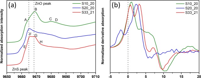
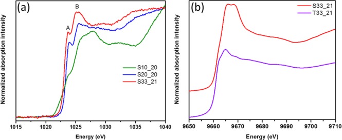
Thinner (2–3 nm) Zn(O,S) films require higher S content to yield similar performances (conversion efficiency) as thicker films, which still lacks a suitable explanation.3 The order of ultrathin Zn(O,S) is not fully developed and the composition is different. S alters the structure and coordination of ZnO, the electrical properties (band gap, alignment and resistivity). Figure 4a reveals similarities between the ultrathin film 10% and ZnO, yet with a more subdued A, B is blue-shifted, and C and D are weaker because of the lack of long-range order. 10% resembles ZnO in literature.14 Decreasing contributions from Zn 4s hybridization with respect to thicker samples impact device characteristics. Increasing S, 20% shows only E and F. An early peak appears (derivative Figure 4b) that shifts the onset earlier, suggesting a lower band gap of the 20% than in the other two compositions. The electron donating behavior of the S ligand20 decreases the Zn–S (increased covalency) and increases Zn–O bond length (increased ionicity). Lack of midrange order and compositional heterogeneity of Zn (increased local distortion) makes this spectrum practically featureless. 33% gets closer to ZnS with less pronounced E than in thicker films. F and G are nearly equivalent. G′s high intensity indicates its higher midrange (20% is featureless in that region, it is most distorted from either crystal structure10). All main peaks shift to slightly higher energy than thick counterparts (Figure 4b and Figure S5a). 33%’s high intensity G is obvious. The shoulders of 10% and 33% are less pronounced than the 20%, where it appears at lower energy and separate in the derivative. The main peak is broadened and at higher energy. The features in the Zn LIII-edge of thin (Figure 5a) and thick samples are aligned with slight intensity differences (Figure S3b). The Zn LIII-edge is less sensitive to changes than the K-edge. The shoulder in thin samples is not visible in thick ones indicating an increase in the number of available states at this shoulder. In thin films, S diffuses toward interfaces forming interfacial sulfate, which was previously observed in the S K edge creating a high energy feature at 2482.5 eV (Figure S5b, S6b) corroborated by ARXPS.10 The Zn LIII edge gives us an indication for the identity of this interfacial sulfate. Peak A (Figure 5a) aligns with ZnSO4,21 possibly sulfate bonded to Zn. A secondary feature seen for ZnSO4 at 1035 eV is not present, contradicting this assumption. Zn may be in two distinct environments defining the A/B distribution, which is different in thinner films. The effect of substrates on the growth Zn(O,S) ultrathin films could not be revealed.10 The Zn K-edge in Figure 5b gives insight into the electronic and geometric structure differences of a 33% sample grown on nanoporous TiO2 NPs and SiO2. The film deposited on titania resembles the thick 33%, which is close to the ZnS (Figure 1a). On SiO2, the spectrum is shifted to higher energies with the first two peaks close in intensity. The nanoporous anatase crystal structure is likely favoring Zn(O,S) crystalline growth given its similarities to ZnS. This is not possible on SiO2. This preliminary substrate-induced growth insight renders further mechanistic reasoning necessary.
Figure 4.
(a) X-ray absorption characterization at Zn K-edge are shown for Zn(O,S) thin films deposited on SiO2. Zn K-edge spectra were background subtracted and atomically normalized in the energy region from 9690 to 9700 eV. (b) Normalized derivative spectra of Zn K-edge.
Figure 5.
(a) X-ray absorption characterization at Zn L-edges is shown for Zn(O,S) thin films deposited on SiO2 (i.e., S10_20:10% pulse ratio on SiO2 substrate, 20 cycles of deposition); (b) X-ray absorption characterization at Zn K-edges are shown for 33% pulse ratio thin films deposited on SiO2 (sample name S33_21) and nanoporous TiO2 (sample name T33_21).
Zn K and L-edges provide insight into finely tuned ALD Zn(O,S) films’ electronic and atomic structure. Differences in ionicity and covalency with O/S were verified regarding one element only. An enhanced shoulder of the main edge in the Zn K-edge with Zn 4s hybridized states shows the wurzite ZnO’s preferred c-axis orientation in the (200) direction. The Zn K-edge of a 2–3 nm thick 10% Zn(O,S) sample has a significantly subdued shoulder, indicating less contribution from Zn 4s hybridization. All spectra have high energy with film thinness suggesting an increase in bandgap. The thin 20% sample seems most distorted with the lowest spectral onset. The Zn K-edge allows us to gather insight into the different growth modes of Zn(O,S) on TiO2 NPs versus SiO2 substrates. The Zn L-edges indicated the formation of ZnSO4 at the interface. Utilizing the metal edge, we provide first time material property knowledge for improving and understanding thin film Zn(O,S)-based solar cell performance characteristics.
Acknowledgments
Use of the Stanford Synchrotron Radiation Lightsource, SLAC National Accelerator Laboratory, is supported by the U.S. Department of Energy, Office of Science, Office of Basic Energy Sciences, under Contract DE-AC02-76SF00515. The Diversifying Academia Recruiting Excellence of Stanford University funded Dr. Orlando Trejo. We thank K. Roelofs and S. Bent for materials. Prof. Torgersen thanks FWF, the Austrian Science Fund: J3505-N20, for the financial support.
Supporting Information Available
The Supporting Information is available free of charge on the ACS Publications website at DOI: 10.1021/acsami.7b06728.
Details of the computational simulations and experimental measurements (PDF)
The authors declare no competing financial interest.
Supplementary Material
References
- Mezher M.; Garris R.; Mansfield L. M.; Horsley K.; Weinhardt L.; Duncan D. A.; Blum M.; Rosenberg S. G.; Bär M.; Ramanathan K.; Heske C. Electronic Structure of the Zn(O,S)/Cu(In,Ga)Se 2 Thin-Film Solar Cell Interface. Prog. Photovoltaics 2016, 24 (8), 1142–1148. 10.1002/pip.2764. [DOI] [Google Scholar]
- Sinsermsuksakul P.; Hartman K.; Bok Kim S.; Heo J.; Sun L.; Hejin Park H.; Chakraborty R.; Buonassisi T.; Gordon R. G. Enhancing the Efficiency of SnS Solar Cells via Band-Offset Engineering with a Zinc Oxysulfide Buffer Layer. Appl. Phys. Lett. 2013, 102 (5), 053901. 10.1063/1.4789855. [DOI] [Google Scholar]
- Platzer-Bjorkman C.; Torndahl T.; Abou-Ras D.; Malmstrom J.; Kessler J.; Stolt L. Zn (O, S) Buffer Layers by Atomic Layer Deposition in Cu (In, Ga) Se 2 Based Thin Film Solar Cells: Band Alignment and Sulfur Gradient. J. Appl. Phys. 2006, 100 (4), 044506. 10.1063/1.2222067. [DOI] [Google Scholar]
- Nakada T.; Kao L.; Jehl Z.; Kobayashi T. A Comparative Study of Heat-Light Soaking Effect on CIGS Thin Film Solar Cells with Zinc Compound Buffer Layers Deposited by ALD and CBD Processes. 28th Eur. Photovolt. Sol. Energy Conf. Exhib. 2013, 2199–2202. 10.4229/28thEUPVSEC2013-3BO.7.5. [DOI] [Google Scholar]
- Schwartz C.; Nordlund D.; Weng T.-C.; Sokaras D.; Mansfield L.; Krishnapriyan A. S.; Ramanathan K.; Hurst K. E.; Prendergast D.; Christensen S. T. Electronic Structure Study of the CdS Buffer Layer in CIGS Solar Cells by X-Ray Absorption Spectroscopy: Experiment and Theory. Sol. Energy Mater. Sol. Cells 2016, 149, 275–283. 10.1016/j.solmat.2016.01.043. [DOI] [Google Scholar]
- Sun S.; Zhang G.; Gauquelin N.; Chen N.; Zhou J.; Yang S.; Chen W.; Meng X.; Geng D.; Banis M. N.; Li R.; Ye S.; Knights S.; Botton G. A.; Sham T.-K.; Sun X. Single-Atom Catalysis Using Pt/Graphene Achieved through Atomic Layer Deposition. Sci. Rep. 2013, 3, srep01775. 10.1038/srep01775. [DOI] [Google Scholar]
- Torgersen J.; Acharya S.; Dadlani A. L.; Petousis I.; Kim Y.; Trejo O.; Nordlund D.; Prinz F. B. Relating Electronic and Geometric Structure of Atomic Layer Deposited BaTiO3 to Its Electrical Properties. J. Phys. Chem. Lett. 2016, 7 (8), 1428–1433. 10.1021/acs.jpclett.6b00393. [DOI] [PMC free article] [PubMed] [Google Scholar]
- Trejo O.; Roelofs K. E.; Xu S.; Logar M.; Sarangi R.; Nordlund D.; Dadlani A. L.; Kravec R.; Dasgupta N. P.; Bent S. F.; Prinz F. B. Quantifying Geometric Strain at the PbS QD-TiO2 Anode Interface and Its Effect on Electronic Structures. Nano Lett. 2015, 15 (12), 7829–7836. 10.1021/acs.nanolett.5b02373. [DOI] [PubMed] [Google Scholar]
- Dadlani A. L.; Trejo O.; Acharya S.; Torgersen J.; Petousis I.; Nordlund D.; Sarangi R.; Schindler P.; Prinz F. B. Exploring Local Electronic Structure and Geometric Arrangement of ALD Zn(O,S) Buffer Layers Using X-Ray Absorption Spectroscopy. J. Mater. Chem. C 2015, 3 (47), 12192–12198. 10.1039/C5TC02912K. [DOI] [Google Scholar]
- Dadlani A. L.; Acharya S.; Trejo O.; Prinz F. B.; Torgersen J. ALD Zn(O,S) Thin Films’ Interfacial Chemical and Structural Configuration Probed by XAS. ACS Appl. Mater. Interfaces 2016, 8 (23), 14323–14327. 10.1021/acsami.6b04000. [DOI] [PMC free article] [PubMed] [Google Scholar]
- Henne B.; Ney V.; Ollefs K.; Wilhelm F.; Rogalev A.; Ney A. Magnetic Interactions in the Zn-Co-O System: Tuning Local Structure, Valence and Carrier Type from Extremely Co Doped ZnO to ZnCo2O4. Sci. Rep. 2015, 5, srep16863. 10.1038/srep16863. [DOI] [PMC free article] [PubMed] [Google Scholar]
- Boichot R.; Tian L.; Richard M. I.; Crisci A.; Chaker A.; Cantelli V.; Coindeau S.; Lay S.; Ouled T.; Guichet C. Evolution of Crystal Structure During the Initial Stages of ZnO Atomic Layer Deposition. Chem. Mater. 2016, 28 (2), 592–600. 10.1021/acs.chemmater.5b04223. [DOI] [Google Scholar]
- Chen H. M.; Chen C. K.; Liu R.; Wu C.; Chang W.; Chen K.; Chan T.; Lee J.; Tsai D. P. A New Approach to Solar Hydrogen Production: A ZnO–ZnS Solid Solution Nanowire Array Photoanode. Adv. Energy Mater. 2011, 1 (5), 742–747. 10.1002/aenm.201100246. [DOI] [Google Scholar]
- Chiou J. W.; Jan J. C.; Tsai H. M.; Bao C. W.; Pong W.-F.; Tsai M.-H.; Hong I.-H.; Klauser R.; Lee J. F.; Wu J. J.; Liu S. C. Electronic Structure of ZnO Nanorods Studied by Angle-Dependent X-Ray Absorption Spectroscopy and Scanning Photoelectron Microscopy. Appl. Phys. Lett. 2004, 84 (18), 3462–3464. 10.1063/1.1737075. [DOI] [Google Scholar]
- Haug J.; Chassé A.; Dubiel M.; Eisenschmidt C.; Khalid M.; Esquinazi P. Characterization of Lattice Defects by X-Ray Absorption Spectroscopy at the Zn K-Edge in Ferromagnetic, Pure ZnO Films. J. Appl. Phys. 2011, 110 (6), 063507. 10.1063/1.3631774. [DOI] [Google Scholar]
- Gilbert B.; Frazer B. H.; Zhang H.; Huang F.; Banfield J. F.; Haskel D.; Lang J. C.; Srajer G.; De Stasio G. X-Ray Absorption Spectroscopy of the Cubic and Hexagonal Polytypes of Zinc Sulfide. Phys. Rev. B: Condens. Matter Mater. Phys. 2002, 66 (24), 245205. 10.1103/PhysRevB.66.245205. [DOI] [Google Scholar]
- Friebel D.; Mbuga F.; Rajasekaran S.; Miller D. J.; Ogasawara H.; Alonso-Mori R.; Sokaras D.; Nordlund D.; Weng T.-C.; Nilsson A. Structure, Redox Chemistry, and Interfacial Alloy Formation in Monolayer and Multilayer Cu/Au (111) Model Catalysts for CO2 Electroreduction. J. Phys. Chem. C 2014, 118 (15), 7954–7961. 10.1021/jp412000j. [DOI] [Google Scholar]
- Li P.; Wang Y.; Chen I.-W. Local Atomic Structure of Pb (Zn1/3Nb2/3) O3 and Related Perovskites I. An Xanes Study of Ionicity/covalency. Ferroelectrics 1994, 158 (1), 229–234. 10.1080/00150199408216021. [DOI] [Google Scholar]
- Rao K. J.; Wong J. A XANES Investigation of the Bonding of Divalent Lead in Solids. J. Chem. Phys. 1984, 81 (11), 4832–4843. 10.1063/1.447509. [DOI] [Google Scholar]
- Dadlani A. L.; Schindler P.; Logar M.; Walch S. P.; Prinz F. B. Energy States of Ligand Capped Ag Nanoparticles: Relating Surface Plasmon Resonance to Work Function. J. Phys. Chem. C 2014, 118 (43), 24827–24832. 10.1021/jp5073044. [DOI] [Google Scholar]
- Mourhatch R.; Aswath P. B. Tribological Behavior and Nature of Tribofilms Generated from Fluorinated ZDDP in Comparison to ZDDP under Extreme Pressure conditions—Part 1: Structure and Chemistry of Tribofilms. Tribol. Int. 2011, 44 (3), 187–200. 10.1016/j.triboint.2010.10.018. [DOI] [Google Scholar]
Associated Data
This section collects any data citations, data availability statements, or supplementary materials included in this article.


