Abstract
We studied the variation of photoresponsivity in multi-layer MoS2 phototransistors as the applied bias changes. The photoresponse gain is attained when the photogenerated holes trapped in the MoS2 attract electrons from the source. Thus, the photoresponsivity can be controlled by the gate or drain bias. When the gate bias is below the threshold voltage, a small amount of electrons are diffused into the channel, due to large barrier between MoS2 and source electrode. In this regime, as the gate or drain bias increases, the barrier between the MoS2 channel and the source becomes lower and the number of electrons injected into the channel exponentially increases, resulting in an exponential increase in photoresponsivity. On the other hand, if the gate bias is above the threshold voltage, the photoresponsivity is affected by the carrier velocity rather than the barrier height because the drain current is limited by the carrier drift velocity. Hence, with an increase in drain bias, the carrier velocity increases linearly and becomes saturated due to carrier velocity saturation, and therefore, the photoresponsivity also increases linearly and becomes saturated.
Background
Recently, transition metal dichalcogenide (TMD) materials including molybdenum disulfide (MoS2) and tungsten diselenide (WSe2) have received considerable attention as the channel material for next generation nanoelectronic devices [1–6]. In particular, thin-film transistors that use MoS2 exhibit interesting electric characteristics such as high electron mobility (~ 200 cm2 V−1 s−1), high current ON/OFF ratio (~ 108), and low subthreshold swing (~ 70 mV dec−1) in a single-layer MoS2 transistor [7]. In addition, MoS2 is attracting attention as a light absorbing layer in optoelectronic devices because of its bandgap energy (single-layer MoS2 has a direct bandgap of 1.8 eV [8] and bulk MoS2 has an indirect bandgap of 1.2 eV [9]) and large absorption coefficient (α = 1–1.5 × 106 cm−1 for single-layer [10] and 0.1–0.6 × 106 cm−1 for bulk [11]). Hence, phototransistors using MoS2 have a low dark current in the OFF state and high photoresponsivity. The performance of MoS2 phototransistors have been improved by introducing an additional layer such as graphene [12–15], quantum dot [16–18], organic dye [19], WS2 [20–22], ZnO [23], and p-type MoS2 [24] or by changing the gate dielectric [7, 25, 26]. In this way, many studies have been actively conducted to improve the photoresponsivity through additional manufacturing processes; however, there is a lack of research on the gain control and specific understanding of MoS2 phototransistors. When gain control is enabled, a wide range of light intensities can be reliably detected, and the gain can be increased without any additional manufacturing process. In this context, we investigated the bias (drain or gate)-controlled photoresponsivity in multi-layer MoS2 phototransistors.
Methods
Figure 1a shows the schematic diagram of the fabricated multi-layer MoS2 phototransistor. We grew the 250 nm SiO2 on a heavily n-doped silicon substrate. The multi-layer MoS2 flakes were mechanically exfoliated from bulk MoS2 (Graphene Supermarket, USA) and transferred to a SiO2/Si substrate by using the conventional scotch-tape method [27]. The source and drain electrodes were patterned by photo-lithography and Ti/Au (5/80 nm) were deposited on the patterned by using an e-beam evaporator. Figure 1b shows the AFM (Atomic Force Microscope) image of the fabricated phototransistor. The channel length and width are 7.31 and 4.74 μm, respectively, and the inset shows the thickness of the multi-layer MoS2 is approximately 49 nm, which corresponds to about 75 layers, assuming the thickness of one layer to be 0.65 nm [28, 29].
Fig. 1.
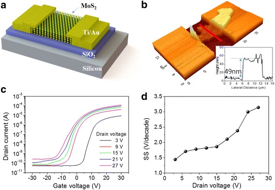
The fabricated MoS2 phototransistor and electrical characteristics. a Schematic diagram of the fabricated multi-layer MoS2 phototransistor. b Atomic Force Microscope (AFM) image of the phototransistor. The inset is the cross-section plot along the red line in the AFM image. c Transfer characteristics of the multi-layer MoS2 phototransistor with the drain voltages of 3, 9, 15, 21, and 27 V in the dark. d Variations in the subthreshold swing with increasing drain bias
Results and discussion
Figure 1c shows the transfer characteristics of the multi-layer MoS2 phototransistor with drain biases of 3, 9, 15, 21, and 27 V in the dark. The current–voltage characteristics of the fabricated multi-layer MoS2 phototransistor were measured using a dual-channel source meter (Keithley 2614B) at room temperature and N2 ambient. The ON/OFF ratio is approximately 105. The field effect mobility was estimated to be 18.6 cm2/V s for a drain bias of 3 V from the following equation [26]:
| 1 |
where L is the channel length, W is the channel width, and the oxide capacitance C OX is 1.38 × 10⁻⁸ F/cm2. It was clearly observed that when the drain bias is increased, the threshold voltage decreases and the subthreshold swing increases. This indicates that the threshold voltage and subthreshold swing are affected by the drain bias. In general, the threshold voltage is estimated by the equation:
| 2 |
where V GS(0) is the intercept between the trend line in a linear part of the transfer curve and the x-axis. However, Eq. (2) assumes a small drain bias such that the velocity saturation effects are negligible (V DS〈〈L ⋅ ν sat/μ eff = 10 V, where ν sat is the saturation velocity and μ eff is the field effect mobility); therefore, it is difficult to extract the exact threshold voltage for a large drain bias. For this reason, we extracted only the change in subthreshold swing and confirmed the effect of the drain bias on the channel. Figure 1d shows the change in subthreshold swing extracted from the slope of the linear part of the log(I D) − (V GS) graph for different drain biases. The subthreshold swing increased from 1.44 V/decade to 3.14 V/decade when the drain bias increased from 3 to 27 V. This implies that a large drain bias lowers the barrier between the MoS2 channel and the Au source electrode, thus weakening the channel controllability of the gate bias.
To investigate the responsivity of the MoS2 phototransistor, we measured the transfer characteristics at various illumination power densities using a 466-nm wavelength diode-pumped solid-state (DPSS) laser. Figure 2a shows the transfer characteristics of the multi-layer MoS2 phototransistor under dark and under three different light intensities (5, 7, and 10 mW/cm2), at a drain voltage of 3 V. As the light intensity increases, the transfer curve shifts to the left, which shows that the photogenerated holes are trapped in the MoS2 channel and act as a positive gate bias [13, 30, 31]. Figure 2b shows that the variation of photocurrent and responsivity when the light intensity and drain bias increase at a constant gate bias of − 30 V. The photocurrent is obtained by the difference between the drain current under illumination and in the dark (I ph = I illuminated − I dark), and the responsivity is defined by I ph/P light, where I ph is the photocurrent and P light is the optical power illuminated on the MoS2 channel. As the drain bias and light intensity increase, the photocurrent and responsivity increase. Considering a laser with a wavelength of 466 nm, the responsivity corresponding to 100% of the external quantum efficiency (EQE) is 0.375 A/W, and the measured responsivity exceeds this value, when the drain bias is 15 V and the light intensity is 8 mW/cm2. This means that there is a photoresponse gain in this multi-layer MoS2 phototransistor and that it is affected by the drain bias.
Fig. 2.
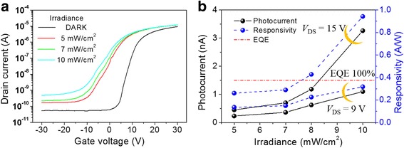
Photoresponse characteristics of MoS2 phototransistors depending on illuminated light intensity. a Transfer characteristics with a constant V DS = 3 V under illumination with three different intensities of light (5, 7, and 10 mW/cm2). b Change in photocurrent with increase in intensity of light when different drain biases (V DS = 9, 15 V) and a constant gate bias (V GS = − 30 V) are applied
In order to observe the change in photoresponsivity according to the gate voltage, we measured the photocurrent while increasing the drain voltage from 3 to 27 V under 5 mW/cm2 light illumination (Fig. 3a). As the applied gate bias increases, the photocurrent increases exponentially in the OFF state (V GS < V th) and becomes saturated in the ON state (V th < V GS). This is because, when the applied gate bias is − 30 V (OFF state) and it is illuminated (Fig. 3b), a large barrier is formed between the MoS2 channel and the source/drain (Au) electrodes. Thus, the electrons needed to maintain the channel neutrality, which was destroyed by the trapped holes, are not well injected into the channel. However, as the gate bias increases up to the threshold voltage, the barrier becomes smaller and the electrons can easily diffuse into the MoS2 channel. Therefore, the photocurrent increases exponentially before the threshold voltage. On the other hand, if the gate bias becomes larger than the threshold voltage, that is, when the device is turned ON, the barrier is sufficiently lowered and the photocurrent is saturated (Fig. 3c). It was also noticed that the photocurrent increases in both the OFF and ON states as the drain bias increases. This means that unlike the photoresponse properties of the conventional phototransistor, which is measured only in the OFF state [26, 32], there is photoresponse gain even in the ON state as the drain voltage increases.
Fig. 3.
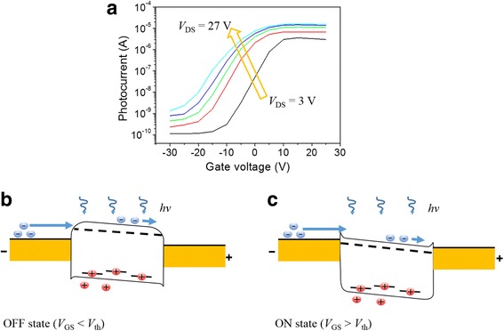
Photoresponse of MoS2 phototransistors depending on applied bias. a Photocurrent at various drain biases (3, 9, 15, 21, and 27 V) and a constant light intensity (5 mW/cm2) depending on the gate bias. b, c The energy band diagrams of a multi-layer MoS2 phototransistor
In order to verify the effect of drain bias on the photoresponsivity of the MoS2 phototransistor in the OFF and ON states, the photoresponse characteristics were measured by illuminating it with light and fixing it to a gate bias of − 30 and 27 V corresponding to the OFF state and ON state, respectively. Figure 4a shows the change in photocurrent, and Fig. 4b shows the responsivity and specific detectivity according to the drain bias in the OFF state. The specific detectivity is extracted from the equation [26, 33]:
| 3 |
where R is the responsivity, A is the area of the MoS2 channel, q is the unit charge, and I dark is the dark current. In the OFF state, the photocurrent and responsivity increase exponentially with a higher drain bias. Therefore, the photocurrent (responsivity), which was 4.28 × 10⁻¹⁴ A (0.12 A/W) when the drain bias was 3 V and light intensity was 10 mW/cm2, increased sharply to 1.57 × 10⁻⁸ A (4.53 A/W) when 27 V drain bias was applied. These results show that the photocurrent and responsivity increase exponentially with the increase in drain bias. On the other hand, in the ON state, the photocurrent (Fig. 4c) and responsivity (Fig. 4d) increase linearly and become saturated as the drain bias increases. When the light intensity is constant at 5 mW/cm2 and the drain bias was increased from 3 to 27 V, the photocurrent (responsivity) increased 5-fold from 2.9 × 10⁻⁶ A (1677 A/W) to 1.5 × 10⁻⁵ A (8667 A/W). Moreover, the detectivity showed the same tendency as responsivity. In the OFF state (Fig. 4b), it increased from 1.76 × 10⁸ Jones to 2.87 × 10⁸ Jones when the drain bias was increased from 3 to 27 V under a light intensity of 10 mW/cm2. In the ON state (Fig. 4d), it increased from 6.14 × 10⁹ Jones to 8.63 × 10⁹ Jones when the drain bias was increased from 3 to 27 V under a light intensity of 5 mW/cm2. Therefore, since the diffusion current is dominant in the OFF state, the responsivity increases exponentially as the drain bias increases. On the other hand, the drift current is dominant in the ON state; therefore, the responsivity increases linearly as the drain bias is increased.
Fig. 4.
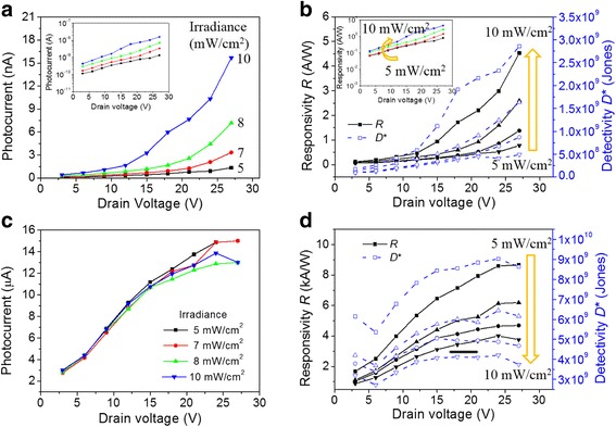
Photoresponse characteristics measured at four different irradiances (5, 7, 8, and 10 mW/cm2) when the drain bias is increased. a Photocurrent, b responsivity, and specific detectivity in the OFF state. Insets in a and b are plotted with the log scale of the photocurrent and responsivity, respectively. c Photocurrent, d responsivity, and specific detectivity in the ON state
The observed drain bias-dependent characteristics of the multi-layer MoS2 phototransistor can be explained by the schematic energy band diagram shown in Fig. 5. When the multi-layer MoS2 channel is illuminated, the electron-hole pairs are photogenerated in the channel. The photogenerated holes are trapped in the MoS2 channel, thus breaking the neutrality of the channel. Then, the positively charged channel attracts more electrons from the source to maintain neutrality, and how much electrons are supplied from the source determines the photoresponse gain. When the applied gate bias is below the threshold, there is a large barrier between the MoS2 channel and the source as shown in Fig. 5a and the drain current is limited by the diffusion over the barrier. As the applied drain bias increases (Fig. 5b), the barrier is lowered due to the bending of the MoS2 channel, thereby facilitating the supply of electrons for channel neutrality. Therefore, as shown in Fig. 4b, the photoresponsivity improves exponentially for the drain bias. When the applied gate bias is above the threshold, the barrier between MoS2 and source is sufficiently low (Fig. 5c), the drain current is limited by the carrier drift in the channel. Therefore, the carrier drift velocity is a major factor in photoresponsivity variation. In this regime, as the applied drain bias increases (Fig. 5d), the carrier velocity and the photoresponsivity linearly increases and saturate at a certain drain bias (~ 10 V) as shown in Fig. 4d.
Fig. 5.
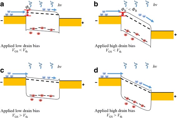
Energy band diagram of multi-layer MoS2 phototransistor under illumination at a low-drain bias in the OFF (V GS < V th) state (a) and a high-drain bias in the OFF state (b). A low-drain bias in the ON (V GS > V th) state (c) and a high-drain bias in the ON state (d)
Conclusions
We fabricated a multi-layer MoS2-based phototransistor and investigated its bias (drain or gate)-controlled photoresponsivity in detail. The change in photoresponsivity according to the bias can be classified into two cases: when the gate bias is smaller than the threshold voltage (OFF state) and when the gate bias is larger than the threshold voltage (ON state). When the gate bias is smaller than the threshold voltage, a small amount of electrons are diffused into the channel, due to large barrier between MoS2 and source electrode. As the gate or drain biases increase, the height of the barrier decreases and the number of electrons injected into the channel for neutrality increases. As a result, the photoresponsivity increases exponentially. On the other hand, when the gate bias is greater than the threshold voltage, the photoresponsivity is affected by the carrier velocity rather than the height of barrier because current is limited by carrier drift velocity. As the drain bias increases, the carrier velocity increases linearly and becomes saturated. Therefore, the photoresponsivity increases linearly and becomes saturated. We were able to understand the responsivity variations in multi-layer MoS2-based phototransistors according to the gate or drain bias. Thereby, the gain can be controlled to increase the range of application of the MoS2 phototransistor and to operate optimally, depending on the purpose and environment.
Acknowledgements
This research was supported by the National Research Foundation of Korea (NRF) grant funded by the Ministry of Education (MOE) (NRF-2017R1D1A1B03034785) and by the Ministry of Science, ICT & Future Planning (MSIP) (NRF-2015M2B2A9033138). This work was also supported by the “Human Resources Program in Energy Technology” of the Korea Institute of Energy Technology Evaluation and Planning (KETEP), granted financial resource from the Ministry of Trade, Industry & Energy, Republic of Korea (no. 20164030201380).
Author’s contributions
JP and YP manufactured the phototransistor. JP and GY measured the phototransistor characteristics. JP, GY, and JH analyzed the measured data. JH planned and supervised the study. All authors read and approved the final manuscript.
Competing interests
The authors declare that they have no competing interests.
Publisher’s Note
Springer Nature remains neutral with regard to jurisdictional claims in published maps and institutional affiliations.
References
- 1.Yoon Y, Ganapathi K, Salahuddin S. How good can monolayer MoS2 transistors be? Nano Lett. 2011;11:3768–3773. doi: 10.1021/nl2018178. [DOI] [PubMed] [Google Scholar]
- 2.Lv R, Robinson JA, Schaak RE, Sun D, Sun Y, Mallouk TE, Terrones M. Transition metal dichalcogenides and beyond: synthesis, properties, and applications of single- and few-layer nanosheets. Acc Chem Res. 2015;48:56–64. doi: 10.1021/ar5002846. [DOI] [PubMed] [Google Scholar]
- 3.Duan X, Wang C, Pan A, Yu R, Duan X. Two-dimensional transition metal dichalcogenides as atomically thin semiconductors: opportunities and challenges. Chem Soc Rev. 2015;44:8859–8876. doi: 10.1039/C5CS00507H. [DOI] [PubMed] [Google Scholar]
- 4.Li H, Wu J, Yin Z, Zhang H. Preparation and applications of mechanically exfoliated single-layer and multilayer MoS2 and WSe2 nanosheets. Acc Chen Res. 2014;47:1067–1075. doi: 10.1021/ar4002312. [DOI] [PubMed] [Google Scholar]
- 5.Jariwala D, Sangwan VK, Lauhon LJ, Marks TJ, Hersam MC. Emerging device applications for semiconducting two-dimensional transition metal dichalcogenides. ACS Nano. 2014;8:1102–1120. doi: 10.1021/nn500064s. [DOI] [PubMed] [Google Scholar]
- 6.Wang QH, Kalantar-Zadeh K, Kis A, Coleman JN, Strano MS. Electronics and optoelectronics of two-dimensional transition metal dichalcogenides. Nature Nanotech. 2012;7:699–712. doi: 10.1038/nnano.2012.193. [DOI] [PubMed] [Google Scholar]
- 7.Radisavljevic B, Radenovic A, Brivio J, Giacometti V, Kis A. Single-layer MoS2 transistors. Nature Nanotech. 2011;6:147–150. doi: 10.1038/nnano.2010.279. [DOI] [PubMed] [Google Scholar]
- 8.Mak KF, Lee C, Hone J, Shan J, Heinz TF (2010) Atomically thin MoS2: a new direct-gap semiconductor. Phys Rev Lett:105, 136805 [DOI] [PubMed]
- 9.Kam KK, Parkinson BA. Detailed photocurrent spectroscopy of the semiconducting group VIB transition metal dichalcogenides. J Phys Chem. 1982;86:463–467. doi: 10.1021/j100393a010. [DOI] [Google Scholar]
- 10.Bernardi M, Palummo M, Grossman JC. Extraordinary sunlight absorption and one nanometer thick photovoltaics using two-dimensional monolayer materials. Nano Lett. 2013;13:3664–3670. doi: 10.1021/nl401544y. [DOI] [PubMed] [Google Scholar]
- 11.Beal AR, Hughes HP. Kramers-Kronig analysis of the reflectivity spectra of 2H-MoS2, 2H-MoSe2 and 2H-MoTe2. J Phys C: Solid Phys. 1979;12:881–890. doi: 10.1088/0022-3719/12/5/017. [DOI] [Google Scholar]
- 12.Hau X, Juanxia W, Feng Q, Mao N, Wang C, Zhang J. High responsivity and gate tunable graphene-MoS2 hybrid phototransistor. Small. 2014;10:2300–2306. doi: 10.1002/smll.201303670. [DOI] [PubMed] [Google Scholar]
- 13.Zhang W, Chuu C-P, Huang J-K, Chen C-H, Tsai M-L, Chang Y-H, Liang C-T, Chen Y-Z, Chueh Y-L, He J-H, Chou M-Y, Li L-J. Ultrahigh-gain photodetectors based on atomically thin graphene-MoS2 heterostructures. Sci Rep. 2014;4:3826. doi: 10.1038/srep03826. [DOI] [PMC free article] [PubMed] [Google Scholar]
- 14.Kwak JY, Hwang J, Calderon B, Alsalman H, Spencer MG. Long wavelength optical response of graphene-MoS2 heterojunction. Appl Phys Lett. 2016;108:091108. doi: 10.1063/1.4943169. [DOI] [Google Scholar]
- 15.Henck H, Pierucci D, Chaste J, Naylor CH, Avila J, Balan A, Silly MG, Asensio MC, Sirotti F, Charlie Johnson AT, Lhuillier E, Ouerghi A. Electrolytic phototransistor based on graphene-MoS2 van der waals p-n heterojunction with tunable photoresponse. Appl Phys Lett. 2016;109:113103. doi: 10.1063/1.4962551. [DOI] [Google Scholar]
- 16.Kufer D, Nikitskiy I, Lasanta T, Navickaite G, Koppens FHL, Konstantatos G. Hybrid 2D-0D MoS2-PbS quantum dot photodetectors. Adv Mater. 2015;27:176–180. doi: 10.1002/adma.201402471. [DOI] [PubMed] [Google Scholar]
- 17.Caiyun Chen, Hong Qiao, Shenghuang Lin, Chi Man Luk, Yan Liu, Zaiquan Xu, Jingchao Song, Yunzhou Xue, Delong Li, Jian Yuan, Wenzhi Yu, Chunxu Pan, Shu Ping Lau, and Qiaoliang Bao. Highly responsive MoS2 photodetectors enhanced by graphene quantum dots. Sci Rep. 2015;5;11830 [DOI] [PMC free article] [PubMed]
- 18.Schornbaum J, Winter B, Schieβl SP, Gannott F, Katsukis G, Guldi DM, Spiecker E, Zaumseil J. Epitaxial growth of PbSe quantum dots on MoS2 nanosheets and their near-infrared photoresponse. Adv Funct Mater. 2014;24:5798–5806. doi: 10.1002/adfm.201400330. [DOI] [Google Scholar]
- 19.Seong Hun Y, Lee Y, Jang SK, Kang J, Jeon J, Lee C, Lee JY, Kim H, Hwang E, Lee S, Cho JH. Dye-sensitized MoS2 photodetector with enhanced spectral photoresponse. ACS Nano. 2014;8:8285–8291. doi: 10.1021/nn502715h. [DOI] [PubMed] [Google Scholar]
- 20.Huo N, Kang J, Wei Z, Li S-S, Li J, Wei S-H. Novel and enhanced optoelectronics performances of multilayer MoS2-WS2 heterostructure transistors. Adv Funct Mater. 2014;24:7025–7031. doi: 10.1002/adfm.201401504. [DOI] [Google Scholar]
- 21.Xue Y, Zhang Y, Liu Y, Liu H, Song J, Sophia J, Liu J, Xu Z, Xu Q, Wang Z, Zheng J, Liu Y, Li S, Bao Q. Scalable production of a few-layer MoS2/WS2 vertical heterojunction array and its application for photodetectors. ACS Nano. 2016;10:573–580. doi: 10.1021/acsnano.5b05596. [DOI] [PubMed] [Google Scholar]
- 22.Yifei Y, Shi H, Liqin S, Huang L, Liu Y, Jin Z, Purezky AA, Geohegan DB, Kim KW, Zhang Y, Cao L. Equally efficient interlayer exciton relaxation and improved absorption in epitaxial and nonepitaxial MoS2/WS2 heterostructures. Nano Lett. 2015;15:486–491. doi: 10.1021/nl5038177. [DOI] [PubMed] [Google Scholar]
- 23.Hsiao Y-J, Fang T-H, Ji L-W, Yang B-Y. Red-shift effect and sensitive responsivity of MoS2/ZnO flexible photodetectors. Nanoscale Res Lett. 2015;10:443. doi: 10.1186/s11671-015-1151-5. [DOI] [PMC free article] [PubMed] [Google Scholar]
- 24.Ye J, Li X, Zhao J, Mei X, Li Q. A facile way to fabricate high-performance solution-processed n-MoS2/p-MoS2 bilayer photodetectors. Nanoscale Res Lett. 2015;10:454. doi: 10.1186/s11671-015-1161-3. [DOI] [PMC free article] [PubMed] [Google Scholar]
- 25.Kim S, Konar A, Hwang W-S, Lee JH, Lee J, Yang J, Jung C, Kim H, Yoo J-B, Choi J-Y, Jin YW, Lee SY, Jena D, Choi W, Kim K. High-mobility and low-power thin-film transistors based on multilayer MoS2 crystals. Nat Commun. 2012;3:1011. doi: 10.1038/ncomms2018. [DOI] [PubMed] [Google Scholar]
- 26.Choi W, Cho MY, Konar A, Lee JH, Cha G-B, Hong SC, Kim S, Kim J, Jena D, Joo J, Kim S. High-detectivity multilayer MoS2 phototransistors with spectral response from ultraviolet to infrared. Adv Mater. 2012;24:5832–5836. doi: 10.1002/adma.201201909. [DOI] [PubMed] [Google Scholar]
- 27.Novoselov KS, Jiang D, Schedin F, Booth TJ, Khotkevich VV, Morozov SV, Geim AK. Two-dimensional atomic crystals. PNAS. 2005;102:10451–10453. doi: 10.1073/pnas.0502848102. [DOI] [PMC free article] [PubMed] [Google Scholar]
- 28.Wakabayashi N, Smith HG, Nicklow RM. Lattice dynamics of hexagonal MoS2 studied by neutron scattering. Phys Rev B. 1975;12:659–663. doi: 10.1103/PhysRevB.12.659. [DOI] [Google Scholar]
- 29.Lee C, Yan H, Brus LE, Heinz TF, Hone J, Ryu S. Anomalous lattice vibrations of single-and few-layer MoS2. ACS Nano. 2010;4:2695–2700. doi: 10.1021/nn1003937. [DOI] [PubMed] [Google Scholar]
- 30.Adinolfi V, Sargent EH. Photovoltage field-effect transistors. Nature. 2017;542:324–327. doi: 10.1038/nature21050. [DOI] [PubMed] [Google Scholar]
- 31.Liu J, Yin Y, Yu L, Shi Y, Liang D, Dai D. Silicon-graphene conductive photodetector with ultra-high responsivity. Sci Rep. 2017;7:40904. doi: 10.1038/srep40904. [DOI] [PMC free article] [PubMed] [Google Scholar]
- 32.Lopez-Sanchez O, Lembke D, Kayci M, Radenovic A, Kis A. Ultrasensitive photodetectors based on monolayer MoS2. Nature Nanotech. 2013;8:497–501. doi: 10.1038/nnano.2013.100. [DOI] [PubMed] [Google Scholar]
- 33.An X, Liu F, Jung YJ, Kar S. Tunable graphene-silicon heterojunctions for ultrasensitive photodetection. Nano Lett. 2013;13:909–916. doi: 10.1021/nl303682j. [DOI] [PubMed] [Google Scholar]


