

Abstract
Power electronics belongs to the future key technologies in order to increase system efficiency as well as performance in automotive and energy saving applications. Silicon is the major material for electronic switches since decades. Advanced fabrication processes and sophisticated electronic device designs have optimized the silicon electronic device performance almost to their theoretical limit. Therefore, to increase the system performance, new materials that exhibit physical and chemical properties beyond silicon need to be explored. A number of wide bandgap semiconductors like silicon carbide, gallium nitride, gallium oxide, and diamond exhibit outstanding characteristics that may pave the way to new performance levels. The review will introduce these materials by (i) highlighting their properties, (ii) introducing the challenges in materials growth, and (iii) outlining limits that need innovation steps in materials processing to outperform current technologies.
Keywords: Silicon carbide, Gallium nitride, Gallium oxide, Diamond, Energy applications
1 Introduction
Automotive and energy saving applications include a number of electronic switching systems capable to distribute electrical power between energy supply, storage, and consumption devices. The performance level may range from (i) low power (10 W to 1 kW) and low voltage (< 400 V) applications like power supplies for consumer electronics and low performance mechatronic systems, via (ii) mid power (1 kW to 100 kW) and mid voltage (400 V to 1.2 kV) applications like electric motor controls, photovoltaic inverters, electric vehicle drives, and universal power supplies to (iii) high power (MW to GW) and high voltage (mainly 1.7 kV to 6.5 kV, but certain devices at higher voltages) applications like rail transport, ships, wind mills, and smart power grid. Basically in all cases the control and transformation of electrical currents (AC → AC, AC → DC, DC → AC, and DC → DC) stand in the foreground.
For high power devices and systems, reliability is the most important issue. Therefore novel materials with extraordinary properties may be used. Opposite, in the low power case, manufacturing costs dominate by far and established mass production processing technologies using standard materials stand in the foreground. In the mid power range, reliability and costs have to be balanced. New technologies are needed but they need to be based on large area, high throughput processing routes.
In power electronics semiconductor diodes and transistors that are able to operate at high voltages, currents, and power densities as well as increasingly higher switching frequencies of several hundred kilohertz are necessary. From a materials perspective the prerequisites may be broken down to three physical properties: (i) a high break down field E B enables electronic devices to withstand high voltages during operation and provides a great robustness against unintentional operation failure, (ii) a large heat‐conductivity λ improves the dissipation of heat loss and lowers the device operation temperature, and (iii) a great charge carrier saturation velocity vs. supports high frequency operation for more efficient electric power converters. Interestingly, those wide bandgap (E G) semiconductors that predominantly exhibit covalent chemical bonds (low ionicity) fulfil these requirements much better than classic semiconductors like Si and GaAs. Table 1 summarizes the key physical properties of the wide bandgap semiconductors SiC, GaN, Ga2O3 and C (= diamond) in comparison to their classic counterparts Si and GaAs.
Table 1.
Physical properties (room temperature values) of wide bandgap semiconductors for power electronic applications in comparison to the classic materials (data from references1, 2, 78)
| SiC | GaN | Ga2O3 | C | Si | GaAs | |
|---|---|---|---|---|---|---|
| EG /eV | 2.3…3.3 | 3.44 | 4.8 | 5.0 | 1.1 | 1.4 |
| EB /105 V·cm–1 | 40 | 60 | 80 | 100 | 4 | 5 |
| λ /W·cm–1 ·K–1 | 3…5 | 1.3 | 0.23 | 20 | 1.5 | 0.5 |
| vs. [107 cm·s–1 | 2.5 | 2.5 | 2 | 2.7 | 1 | 2 |
| Lattice parameter | ||||||
| a /Å | 3.08 (hex) | 3.19 | 12.23 | 3.57 | 5.43 | 5.65 |
| b /Å | 3.04 | |||||
| c /Å | 5.80 | |||||
| β /° | 103.7 | |||||
| T S /°C | 2830 | 2500 | 1940 | 3900 | 1420 | 1250 |
Typically, the wide bandgap semiconductors summarized in Table 1 exhibit a small lattice parameter and a high melting or dissociation temperature T S. In reciprocal space (k‐space) this leads to an energy dispersion E(k) of the valence and conduction bands represented by a large effective electron (hole) mass and, hence, a low intrinsic charge carrier mobility. Irrespective of this, due to the great charge carrier saturation velocities vs > 2 × 107 cm·s–1 as well as due to the break down field values E B > 40 × 105 V·cm–1, these wide bandgap materials meet the requirements for high frequency electronic device operation.
Related to the short bond lengths in the crystal structures as well as related to the strong chemical bonds, all wide bandgap materials in Table 1 exhibit elevated dissociation temperatures. While Ga2O3 may be grown from a stoichiometric melt, all other semiconductors, i.e. SiC, GaN, and C (diamond) need special vapor growth techniques or other high pressures processes under harsh environments as described in the forthcoming sections.
Another typical feature of the wide bandgap materials in Table 1 is the occurrence of various stable crystal polytypes.
(i) The most prominent example is silicon carbide that exhibits a large number of different stacking sequences of the Si–C double layers. In these structures, each Si is surrounded by four C atoms and vice versa. Physically mainly the electronic bandgap as well as the charge carrier mobility μ varies (Table 2), although the cubic 3C‐SiC polytype also exhibits a slightly lower breakdown field (Table 2).
Table 2.
| 4H‐SiC | 6H‐SiC | 3C‐SiC | 15R‐SiC | |
|---|---|---|---|---|
| E G /eV | 3.23 | 3.98 | 2.36 | 2.96 |
| E B /105 V·cm–1 | 40 | 25 | ||
| μ n /cm2 ·V–1 ·s–1 | 400 | 300 | 900 | 800 |
(ii) In the case of gallium nitride two polytypes are observed: The technological relevant hexagonal, chemically stable 2H‐GaN as well as the metastable 3C‐GaN counterpart.
(iii) Although electronically quite different, diamond (sp3 carbon) and graphite (sp2 carbon) may also called a polytypic variation of crystalline carbon.
(iv) In the case of gallium oxide the monoclinic, so called β‐Ga2O3, is the most important crystal structure with respect to electronic applications.
In the following review, each materials section on SiC, GaN, Ga2O3, and Diamond starts with historic remarks that conduct its discovery or materials development. A brief description of the phase diagram of the material is followed by an introduction into the growth methods applied for the processing of single crystalline boules. Finally, special materials issues and applications are highlighted. Materials‐wise, the section on SiC significantly includes own research results of the author with special emphasis on large area growth of SiC as well as in‐situ process visualization of the growth process. In the case of the sections on GaN, Ga2O3, and Diamond the review is mainly based on literature data.
2 Silicon Carbide
In terms of novel semiconductor materials beyond silicon for power electronic devices, silicon carbide exhibits the most mature technology with fast growth market share. High performance device operation is limited by the provision of semiconductor wafers with low defect densities. Both, improvement of the crystal growth technology as well as deepening of the fundamental understanding of the crystal growth process are mandatory to make full use of the extraordinary physical properties of SiC as listed in Section 1.
2.1 Phase Diagram and Growth Methods of Silicon Carbide
Figure 1 shows the phase diagram of silicon carbide with its peritectic decomposition of the stoichiometric SiC phase at ca. 2830 °C.3
Figure 1.
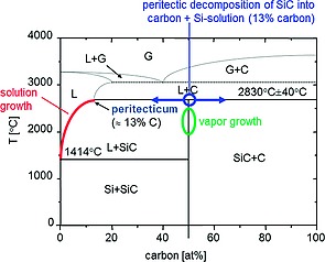
Phase diagram of SiC and routes of crystal growth using sublimation or solution growth.
Hereby SiC decomposes into carbon and a silicon rich solution of up to 13 at % of carbon. In crystal growth technology SiC boules are mainly grown from the vapor by the so called physical vapor transport (PVT) method (Figure 2). Sublimation of stoichiometric SiC source material (usually SiC powder) is carried out at elevated temperatures above 2000 °C in an inductively heated closed graphite crucible surrounded by graphite foam or felt as isolating material. Crystallization is conducted at slightly lower temperatures (e.g. ΔT = 50 °C) on a mainly (0001) oriented seed crystal. Today, this technology may be called mature, although crystal size enlargement from currently 100 mm to 150 mm and even 200 mm as well as reduction of the defect density and strain related wafer bow are challenging issues. The development of the PVT technique may be traced back to the fundamental works of Lely,3 Tairov, and Tsvetkov,4 as well as Ziegler et al.5 In order to establish the SiC mass transport from the bottom of the crucible (SiC powder source) to its top (crystal growth interface), an axial temperature gradient is mandatory. Since the mass transport is initiated by a temperature gradient, the growing crystal by default will be exposed to thermally induced stress in axial as well as radial direction. The reduction of defect density needs to account for this intrinsic boundary condition.
Figure 2.

Schematic sketch of a growth cell for the processing of SiC using the physical vapor transport method.
The applied graphite parts usually exhibit a porosity of at least a few percent and therefore feature a permeable behavior for inert gases like argon and nitrogen. Therefore, n‐type doping using the donor nitrogen in SiC may be carried out simply by the supply of nitrogen gas into the growth chamber. In the case of p‐type doping using the acceptor boron or aluminum solid sources that are sublimed as addition to the SiC powder source or from an external dopant reservoir6, 7 are applied. While n‐type doping using nitrogen gas is well controlled, in particular p‐type doping using aluminum is quite challenging. Due to its much higher partial pressure than SiC at growth temperature, feeding of the dopant through an extra pipe into the growth cell is necessary.7
At temperatures between 2000 °C and 2400 °C the gas phase of the subliming SiC powder is composed of mainly Si, Si2C, and SiC2 but hardly of SiC molecules.8 By the application of the inert gas argon (pressure = 10 mbar to 50 mbar) the growth process may be conducted in diffusion limited mode. Typical growth rates lie between ca. 200 μm·h–1 and 300 μm·h–1 and may be as much as 500 μm·h–1 to 1000 μm·h–1 but with increasingly challenge with increasing growth rate to obtain uniform material. A critical issue is the minimization of the radial temperature gradient in order to keep the residual sheer stress in the growing crystal as low as possible. The control of the temperature and the partially related gas species concentration fields are the main objectives during growth process optimization.9, 10, 11, 12, 13, 14 For a review it is related to reference15.
Related to the PVT process a high temperature chemical vapor deposition (HT‐CVD) technique has been developed16, 17 that also operates above 2000 °C. Instead of SiC as source material, HT‐CVD makes use of gaseous precursors like silane (SiH4) and ethylene (C2H4) that decompose at elevated temperature to form SiC clusters that act as sublimation source for the growth of the SiC boule. The technologic strength to apply HT‐CVD lies in the advanced p‐type doping capability using aluminum precursors like tri‐methyl‐aluminum (TMA) as well as in the fabrication of high purity SiC boules. Challenges features are achieving continuous growth at high growth rates as well as suppressing unintentional secondary deposits. Compared to PVT, the handling of toxic gases causes higher operation costs during operation of HT‐CVD.
The other SiC growth route is based on crystallization from a Si‐rich Si‐C solution. The addition of further elements to enhance the carbon solubility may be applied. Within the last two decades significant progress in solution growth has been achieved. Initial studies of growth on 2 inch SiC seeds were done by Hofmann and Müller 18 and refined by Epelbaum et al.19 The control of the carbon concentration in the Si‐based melt and the transport of carbon to the growth interface require special attention during solution growth. Often graphite crucibles are applied, which are intentionally partially dissolved by the silicon solvent. Noteworthy is that the wetting behavior of silicon based solutions strongly depends on the graphite micro‐morphology. Despite all experimental obstacles, an increasing number of research reports in recent years (see, for example20, 21) demonstrate how the fundamental understanding the SiC solution growth process significantly improved.
Most reports on solution growth follow the top seeded solution growth (TSSG) approach at temperatures below 2000 °C that use metal additives like Cr, Ti, and Al to increase the carbon solubility in the Si melt. At these temperatures the lower Si partial pressure enables a growth configuration based on a classic Czochralski setup. Using Si‐Cr and Si‐Ti solution at a growth temperature of 1940 °C, Kusunoki et al.21 reported for a crystal diameter of 75 mm a growth rate of 200 μm·h–1. In the case of smaller crystal diameters, growth rates above 1 mm·h–1 were reached. In general, during solution growth of SiC, metal additives are incorporated up to their solubility limit into the SiC crystal, which may alter the electronic properties of the semiconductor substrate. Recently it was reported from the author's team that the vertical Bridgman / vertical gradient freeze method can be applied at temperatures as high as 2300 °C using a metal free silicon‐carbon solution of very high purity to perform SiC solution growth.22 This growth configuration could solve the current challenge of unintentional doping of the SiC crystal by the metal additives during solution growth based on the Czochralski‐like process.
The growth from the melt is carried out close to thermodynamic equilibrium and therefore usually leads to a lower dislocation density than other methods like PVT. Using solution growth a high structural quality of SiC23 and the possibility to close micropipes was demonstrated.19, 24 Whether the application of solution growth will eventually lead to the fabrication of large area 4H‐SiC boules for power electronic applications cannot be foreseen today. In the author's opinion, key points for the commercial success of solution growth of SiC crystals are the realization of long term stable growth conditions for the growth of long crystal boules as well as the cost reduction by an efficient re‐usage of the crucible materials and the solvent Si.
2.2 In‐situ X‐ray Visualization of the Growth Process
The closed graphite crucible exhibits a rather limited growth process control. Temperature measurements using optical pyrometers at the top as well as at the bottom of the crucible and numerical simulation of the temperature field are used to derive the conditions inside the growth cell. The reliability of these data, however, strongly depends on the knowledge of the thermal and electrical properties of the graphite components and the SiC source material. A real drawback compared to the Czochralski growth process of Si is the lack of an optical access to the crystal growth context. In this context, the development of in‐situ 2D and 3D X‐ray based monitoring25, 26, 15 has significantly improved the control of the growth process. Besides the crystal growth interface, major insight into the sublimation‐recrystallization and related materials densification of the SiC source material has been achieved. In its most advanced stage, in‐situ 3D X‐ray computed tomography is applied (Figure 3).15
Figure 3.

Sketch of the setup to visualize the PVT growth process using in‐situ X‐ray computed tomography.
The growth cell is rotated continuously or in a number of single steps during the in‐situ visualization, while simultaneously acquiring 2D X‐ray projection images (Figure 3). Applied to a PVT growth machine for the growth of 3 inch SiC crystals, a tungsten X‐ray source (DC voltage = 125 kV peak, maximum cw current = 350 μA, spot size = 70 μm,) and a flat panel X‐ray detector [PaxScan 2520D/CL, Varian Medical Systems, CsI scintillator layer, active matrix of 1496 × 1874 pixels, pitch size = 127 μm2 (3.94 lp·mm–1)] are used for high throughput image acquisition. With a frame rate of up to 30 fps in a 2 × 2 binning mode (10 fps without binning) the so called fly‐by‐measurements were carried out where the growth setup is continuously rotated during data acquisition. In the standard mode 2D X‐ray images are collected in a stop‐and‐go‐mode. The 3D image processing is conducted using a series of 200 to 400 2D X‐ray projection images in conjunction with the classic so called filtered back‐projection Feldkamp‐algorithm.27 The typical 3D image acquisition time lies between 3 min and 15 min. The special resolution of the setup is ca. 125 μm (voxel size). At typical crystal growth rates between 200 μm·h–1 and 500 μm·h–1 3D the image acquisition is performed without further spatial resolution losses.
Figure 4 shows a series of in‐situ 3D views into the hot crystal growth cell at ca. 2200 °C. Within this overview‐projections the crystal growth process (enlargement of the crystal height) as well as the consumption of the SiC powder in the periphery of the crucible is clearly observed after 28 h, 52 h, 78 h, and 100 h. For a further analysis 2D image cuts from the 3D computed tomography data set can be used (see, for example reference15). Detailed studies of the SiC powder consumption have been carried out recently as the source material consumption is the main limit for long growth periods.28 While the advanced 3D X‐ray computed tomography enables fundamental research studies, the less complex 2D X‐ray visualization25 may be applied during standard crystal growth in a production environment.
Figure 4.

A series of live images of the PVT growth process at ca. 2200 °C acquired using in‐situ X‐ray computed tomography.
2.3 The Hexagonal 4H‐SiC Polytype
Growth of 4H‐SiC for power electronic applications is performed on (000–1) oriented carbon face seeds (Figure 5). In some cases, 2° or 4° off oriented seeds are applied. The 4H‐SiC polytype stability is observed in a C‐rich gas phase composition at higher supersaturation compared to the growth of 6H, i.e. higher axial temperature gradient compared to the average temperature.29 In the case of diffusion limited growth using argon inert gas, no polytype stability dependence on the inert gas pressure has been reported so far.29 Nitrogen doping stabilizes the growth of 4H‐SiC boules.30 Crystal defects in the SiC crystal that limit the electronic device operation include dislocations, stacking faults, carbon inclusions, and silicon droplets as well as macroscopic hollow core defects.31 It has been reported that basal plane dislocations dramatically limit device stability of bipolar diodes. Bergman at al.32 reported an electron‐hole‐pair‐recombination driven enhancement of stacking fault generation, which strongly deteriorates the bipolar device performance. Unipolar devices like Schottky diodes are altered by threading screw dislocation densities.33 Threading screw dislocations and in particular basal plane dislocations cause a device breakdown along the metal oxide / SiC interfaces.34 Micropipes that mainly stem from threading screw dislocations35, 36 cause immediate device failure. From this list it follows that the reduction of the dislocation density is the main task during crystal growth. In this context tailoring of the temperature field in terms of low radial gradients throughout the complete process time as well as during cooling down of the crystal after growth are the main challenges. Numerical simulation of the steady state and transient temperature fields inside the growth cell are key issues. Experimentally the process control is carried out by the setting of the inductive heating power and the simultaneous monitoring of the temperature at the top and bottom of the growth cell. Process optimization is carried out in an iterative sequence of numerical simulation of the temperature field, step‐by‐step tailoring of the geometry of the growth cell and application of the adapted growth configuration to experiments. Figure 5 shows an optical image of an as grown 100 mm single crystal that has been oxidized to remove residual carbon from the crystal surface. The various colors are related to a thin SiO2 surface layer.
Figure 5.

Optical image of an as grown 100 mm single crystalline 4H‐SiC boule.
2.4 The Cubic 3C‐SiC Polytype
Since the beginning of research and development of the semiconductor SiC, the cubic polytype 3C‐SiC has been of particular interest due to its higher electron mobility compared to the hexagonal 4H‐SiC (Table 2). In addition, due to lower bandgap of E g(3C‐SiC) = 2.3 eV versus of E g(4H‐SiC) = 3.2 eV, its metal SiO2 semiconductor (MOS) interface exhibits a significantly lower defect density, which is beneficial for metal oxide semiconductor field‐effect transistor (MOS‐FET) applications.37, 38, 39 Recent results have demonstrated a MOSFET channel mobility of 300 cm2 /Vs for 3C‐SiC, which outperforms the 4H‐SiC counterpart with a channel mobility below 100 cm2 ·cm–1. Compared to 4H‐SiC, however, polytype stability during 3C‐SiC bulk growth is much lower and therefore the crystal defect density much higher. Among others, proper growth parameters of 3C‐SiC include a high supersaturation, a high temperature gradient and a silicon rich gas phase. So far basically no large area seeds are available. The difficulties to realize bulk 3C‐SiC may be related to a challenging nucleation and preservation of the 3C‐SiC polytype. Besides polytype changes, stacking faults (SFs), double positioning grain boundaries (DPBs) and antiphase boundaries (APBs) are the most prominent defects known in 3C‐SiC. Due to all of the growth obstacles, it was considered from the beginning of 3C‐SiC growth development on to perform heteroepitaxial bulk seeding either on (100) or (111) 3C‐SiC epitaxial layers that were fabricated on (100) or (111) Si substrates or bulk seeding on hexagonal (0001) oriented 6H‐SiC and 4H‐SiC substrates.
Beside this, various approaches have been followed in recent years to grow bulk or at least bulk‐like 3C‐SiC (see, for example, references40, 41, 42, 43, 44, 45, 46, 47, 48, 49, 50, 51, 52). All these studies have established a broad knowledge for the successful growth of 3C‐SiC bulk material. Together with great advances in growth reactor technology first large area, bulk‐like 3C‐SiC was demonstrated recently by the author's team. The PVT‐like growth of (100) 3C‐SiC is carried on (100) 3C‐SiC‐on‐Si seeding layer fabricated by chemical vapor deposition (CVD). A critical step in this technology is the transfer of the thin 3C‐SiC seeding layers (thickness ca. 12 μm to 50 μm) from the silicon wafer to a high temperature stable carrier. Figure 6 illustrates the transfer process that consists etching of the Si‐wafer using a HNO3 + HF solution, deposition of a carbon glue on top of the 3C‐SiC layer and mechanical transfer to a poly‐crystalline SiC carrier.53, 54 The resulting seeding stack was used in a subsequent PVT‐like growth process to form quasi bulk 3C‐SiC of an area of up to 10.5 cm2 and a thickness of up to 0.9 mm (Figure 7).53, 54 The 3C‐SiC was free of double position and antiphase boundaries and exhibited no polytype switches. The presented result is believed to be a major step towards real bulk 3C‐SiC in the near future.
Figure 6.

Seed preparation for 3C‐SiC growth on 3C‐SiC‐on‐Si CVD seeding layers.
Figure 7.

Optical image of an as grown yellow 3C‐SiC bulk like crystal (area = 10.5 cm2, thickness = ca. 0.5 mm) on its green 6H‐SiC carrier.
2.5 The Rhombohedral 15R‐SiC Polytype
Another high potential silicon carbide polytype is the rhombohedral 15R‐SiC. This polytype exhibits an even greater electron mobility than cubic 3C‐SiC (Table 2) and a lower bandgap than 4H‐SiC. It may be grown in a quite narrow process window on the Si face of (0001) hexagonal SiC in a Si‐rich gas phase environment.55 Despite its great potential in power electronic application, this polytype is currently solely under fundamental academic investigation.
2.6 Novel Applications of SiC
Other than power electronic applications, the hexagonal and cubic SiC polytypes have recently shown new high potential applications.
Co‐doping of 6H‐SiC and 4H‐SiC with nitrogen and boron as well as nitrogen and aluminum showed its great applicability as fluorescent SiC in white LED application.56, 57
Cubic silicon carbide doped with the deep boron acceptor is a candidate for an intermediate band solar cell material with theoretical light conversion efficiencies above 50 %.58, 59
Finally, p‐type 3C‐SiC doped with aluminum is currently studied for the application in solar driven water splitting.60, 61
The success of SiC in these various high potential applications depends much on the progress in materials preparation. Recent advances in 3C‐SiC may pave the way for a number of new applications of SiC beside the technology‐driver of power electronics.
3 Gallium Nitride
3.1 Phase Diagram and Growth Methods of GaN
In the case of GaN the high partial pressure of nitrogen of ca. 4.5 × 10³ MPa at the materials dissociation temperature of ca. 2500 °C is the characteristic feature that routes potential growth techniques. Although AlN has no obvious application in power electronic devices so far, it is worth summarizing its bulk growth capabilities with respect to a potential transfer to GaN. The dissociation temperature of crystalline AlN lies around 3200 °C, however, the nitrogen decomposition pressure of ca. 20 MPa is quite low compared to 4.5 × 10³ MPa in case of GaN. Like in the case of SiC, AlN single crystals may be processed by the physical vapor transport method.62, 63, 64 A significant number of current growth studies are carried out by teams that also investigated SiC bulk growth in the past. As crucible materials either tungsten or tantalum (tantalum carbide) are used. Special emphasis has to be put on the purity of the AlN powder source material. In particular the oxygen contamination needs to be lowered as much as possible. The applied crucible material impacts the gas phase chemistry. In the case of tungsten, growth is carried out on (0001) N‐polar seeds. A significant crystal diameter reduction occurs during sublimation growth that causes the need to use foreign substrates like 6H‐SiC wafers and hetero‐epitaxial seeding with its drawback of initially high dislocation density in the AlN crystal boule. Growth in tantalum (or tantalum carbide) crucible may be carried out on (0001) Al‐polar seeds that enables a radial extension of the single crystal diameter and may be favored for homo‐epitaxial seeding on AlN wafers. A drawback of the tantalum based crucible system is the lower crystal purity, which causes strong optical below bandgap absorption in the ultraviolet light spectrum for the material.
As pointed out above, in the case of GaN the nitrogen component exhibits a much higher partial pressure at the dissociation temperature compared to AlN. In practice, classic physical vapor transport cannot be applied as bulk growth method for GaN above 2000 °C. In the past, PVT related growth has been proposed65 but did not succeed so far on a large scale. The best single crystalline GaN boules have been prepare by the hydrogenated vapor phase epitaxial growth (HVPE)66, 67 and by the ammonothermal crystallization under ammonobasic conditions.68, 69
While in particular power opto‐electronic laser and light‐emitting diodes benefit from bulk GaN seeding wafers, for power electronic applications another approach is favored (which is based on hetero‐epitaxial growth of GaN on large silicon wafers). Due to the quite low heat conductivity of GaN that blocks heat dissipation during power electron device operation, the major application field of GaN lies in the lower voltage range between 200 V and 600 V, which basically bridges between the semiconductors Si (low voltage, 200 V to 400 V) and 4H‐SiC (high voltage, 1200 V and above). This voltage range targets electronic devices for automotive and energy applications that face extreme cost pressure. In this context the hetero‐epitaxial processing of GaN layers on large area Si wafers is coherent. It is noteworthy that the cubic 3C‐SiC polytype semiconductor aims into the same 600 V device application. The material GaN, however, profits if high device switching frequencies are needed rather than if power comes to the fore.
3.2 Growth of GaN on Si‐Seed‐Wafers
A major breakthrough to process GaN epitaxial layers on (111) Si‐wafers was developed by Dadgar, Krost et al.70, 71, 72 Their development is based much on fundamental studies by Watanabe, Amano, Akasaki et al.73, 74 and Hearne et al.75
The (111) orientation of Si is applied as substrate to force the hetero‐epitaxial nucleation of the hexagonal 2H‐GaN polytype. Besides the lattice mismatch between Si and GaN of ca. 16 %, the difference in thermal expansion α is the more serious problem. As a consequence, optimization of the growth of GaN on Si is inherent with tailoring of residual layer GaN stress towards residual compressive strain that inhibits layer cracking.
GaN exhibits a larger α‐value than Si; i.e. α(GaN) = 5.59 × 10⁻⁶ K–1 (T = 300 K to 900 K)76 vs. α(Si) = 3.77 × 10⁻⁶ K–1 (T = 300 K to 900 K),77 which causes tensile stress in the hetero‐epitaxially grown GaN layer after cooling down to room temperature. As a consequence, GaN layer cracking is a severe problem. For comparison please note: The standard GaN substrate exhibits an α‐value of α(GaN) = 7.5 × 10⁻⁶ K–1,76] which causes compressive strain in the epitaxial layer without cracking.
Watanabe, Amano, Akasaki, and their co‐workers73, 74 introduced the application of low temperature grown, thin AlN interlayers (= LT‐AlN) to compensate in grown stress in the GaN from tensile to compressive strain. Dadgar, Krost, and their co‐worker70, 71 basically integrate two ca. 40 nm thin LT‐AlN interlayers into three ca. 400 nm thick high temperature grown GaN layers (= HT‐GaN) to achieve compressive strain and basically leading to no cracking in GaN material on Si.
Dadgar, Krost, and their co‐workers72 carried out an additional key development. Doping of GaN is usually carried out by Si through an addition of silane (SiH4) to the epitaxial GaN growth process. In highly n‐type doped GaN layers, however, this may lead again to tensile stress and cracking in the epitaxial film. Through the exchange of the dopant Si by Ge using germane (GeH4) as doping gas the compressive GaN layer strain could be preserved and cracking was inhibited. In addition, greater layer conductivities could be realized through the usage of Ge as donor.
The combined tailoring of GaN epitaxial films grown on (111) Si through the addition of LT‐AlN interlayers and through the replacement of Si n‐type doping of GaN using Ge are key features for a technologic application of GaN films on Si‐wafers.
4 Gallium Oxide
4.1 Phase Diagram of Growth Methods of Gallium Oxide
Like the standard semiconductor silicon, gallium oxide may be grown from the melt. The high melting point of T = 1940 °C makes great demands on the growth setup and in particular on temperature stability and chemical inertness of the melt carrying crucible material.
First reports on melt growth of Ga2O3 stem from Chase et al.79 Lorenz et al.,80 and Harwig et al.81 who applied the quasi crucible free Verneuil process to fabricate crystals of up to 10 mm in diameter and 25 mm in length for fundamental studies of structural, electrical and optical materials properties.
Current studies follow either the crucible free floating zone process (see Section 4.2) or crucible based Czochralski method with its derivative, the edge defined film‐fed growth (section 4.3).
4.2 Floating Zone (FZ) Growth of Ga2O3
In recent years, the crucible free floating zone (FZ) growth process has been applied by a number of research groups.82, 83, 84, 85, 86, 87 Like in the case of a number of oxide materials, intense light of halogen lamps and a focusing ellipsoidal mirror system is used for heating. As source material a rod of isostatically pressed Ga2O3 powder (typical purity: 4 N to 5 N) is applied. The largest Ga2O3 crystals exhibit a diameter of 25 mm and a length of 40 mm.85 To reduce the concentration of oxygen vacancies that form intrinsic donors in Ga2O3, an annealing process in an oxygen‐rich atmosphere may follow the growth process. To achieve larger crystal diameters of 100 mm or better 150 mm that meet the requirements for the processing of electronic devices, crucible based growth technologies (section 4.3) may be favorable for Ga2O3.
4.3 Czochralski (CZ) and Edge‐Defined Film‐Fed (EFG) Growth of Ga2O3
In the case of the crucible based Czochralski (CZ) process88, 89, 90 and its related derivative the edge‐defined film‐fed (EFG) growth technique91 iridium is applied to carry the Ga2O3 melt. To suppress oxygen evaporation from the melt as well as the decomposition of the crucible material, a gas mixture of argon and oxygen or argon and carbon dioxide is applied under ambient pressure. Related to the pronounced (100) and (001) cleavage planes of the monoclinic β‐Ga2O3 lattice, growth is performed in the crystallographic [010] direction. To reduce thermal stress, cooling down the crystal to room temperature is usually carried out using an after‐heater.
Using the Czochralski method88, 90 crystals of up to 100 mm in diameter78 have been prepared. In the case of the EFG‐process91 flat (100) oriented 150 mm large quasi‐wafers have been fabricated78 that meet basic technological device processing requirements.
4.4 Outlook
The main obstacles to be solved for the growth of Ga2O3 single crystals for a broad technical application are related (i) to the control of oxygen partial pressure, and (ii) the presence of the pronounced (100) and (001) cleavage planes.
In the case of the oxygen partial pressure a suppression of oxygen evaporation from the Ga2O3 melt is necessary to inhibit a nonstoichiometric composition of it as well as the corrosion of the iridium crucible. Also an evaporation of oxygen from the Ga2O3 crystal surface during growth and during cooling down needs to be further suppressed in order reduce unintentional doping through intrinsic oxygen vacancies.
In the author's opinion, melt growth of Ga2O3 by the vertical Bridgman (VB) and Vertical Gradient Freeze (VGF) should be considered in the future. Low temperature gradients during growth could lower the probability of cleavage along (100) and (001) planes. In addition, the usage of a liquid encapsulation (to be developed) on top of the melt surface would minimize the oxygen vacancy generation in the crystal and the oxygen corrosion problem of the iridium crucible.
5 Diamond
5.1 Phase Diagram and Growth Methods of Diamond
The phase diagram of the existence range of the carbon crystal structures graphite and diamond as a function of temperature and pressure in Figure 8 exhibits a number of features relevant for selection of the growth process. Although quite stable under ambient conditions and temperatures up to ca. 1000 °C, diamond may be accounted as metastable phase of carbon with graphite as stable structure under ambient pressure. Graphite dissociates at ca. 3900 °C and a pressure of up to ca. 100 MPa directly into gaseous carbon with no intermediate liquid phase. Diamond itself exhibits an equilibrium transition into liquid carbon at ca. 4000 °C and a pressure of ca. 104 MPa. With increasing pressure to values above 5 × 10³ MPa the melting point of diamond lowers to values below 2000 °C.
Figure 8.

Sketch of the phase diagram of carbon as a function of temperature and pressure.
Based on the phase diagram in Figure 8 growth of crystalline diamond may be performed under equilibrium‐near conditions from a carbon melt or solution at extreme pressures in the 5 × 10³ MPa range that touch technological limits. In this context the high pressure high temperature solution growth (HPHT) has been developed.92, 93, 94 Using for example carbon in an iron‐nickel alloy as catalyst at 5.5 × 10³ MPa and 1300 °C diamond of up to a few millimeters in size have been synthesized.95 The crystal size is much limited by the dimension of the vessel interior that needs to withstand the extreme pressure of ca. 5 × 10³ MPa.
5.2 Gas Phase Deposition of Diamond
Another approach to grow crystalline diamond is based on off‐equilibrium conditions during vapor growth.92, 93, 94, 96, 97, 98, 99 In particular, chemical vapor deposition (CVD) that makes use of hydrocarbon precursors like methane (CH4), ethane (C2H4), and propane (C3H8) is applied.
Stability criteria to perform chemical vapor deposition of diamond are given by the Bachmann triangle C‐H‐O composition diagram (Figure 9). In particular, the hydrocarbon route C‐H needs hydrogen rich conditions with at least 97 % of H2 in the case of a CH4 precursor diluted in H2. The high hydrogen content inhibits that formation of graphite by predominantly etching of sp2‐bound carbon vs. sp3‐bound carbon in the diamond case.
Figure 9.
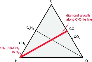
Sketch of the Bachmann triangle C–H–O composition diagram for stable diamond growth conditions. Red lines indicate areas of diamond deposition.
Noteworthy is so called the CO tie line within the Bachmann triangle that offers additional technologic freedom in future development of diamond growth processes. In the hydrocarbon route, growth kinetic of diamond mainly depends on (i) the availability of atomic hydrogen (elemental H) and the methyl radical (CH3), as well as on (ii) the provision of carbonized seeding interface. Technically, the dissociation of hydrogen gas (H2) into hydrogen radicals (elemental H) and hydrocarbons (CH4, C2H4, C3H8) into methyl radicals (CH3) precursors is performed through a hot filament (T ≈ 2000 °C) of tungsten (alternative: tantalum), by the provision of microwave heated plasma or by usage of a hot thermal plasma jet gas stream.
As seeds carbonized metal (e.g. Ir, Fe) and silicon surfaces or diamond platelets may be applied that are chemically stable in the harsh environment of the hydrogen and methyl radicals. Recently, Mühle et al.100 demonstrated a diamond single crystal of ca. 7 × 7 × 1.5 mm3 in size that was grown on a 3 × 3 × 1.4 mm3 HPHT diamond seed using a 2.45 GHz microwave CVD reactor (substrate temperature of 1000 °C to 1200 °C, pressure ca. 200 mbar) at a growth rate of ca. 18 μm·h–1.
5.3 Doping of Diamond
Like in the case of the group IV semiconductor silicon, the small boron atom may be applied as acceptor dopant. Due to the large hole binding energy of ca. E A ≈ 400 meV, the electrical activation at room temperature is rather low. Doping with donors, however, is an unsolved issue in diamond. Phosphorous and nitrogen that are quite successfully used as donors in silicon and silicon carbide, respectively, fail in diamond.
6 Summary
Among the presented wide bandgap semiconductors the hexagonal 4H‐SiC already offers a mature bulk crystal growth and device processing technology. Its major application lies in the field of high power electronics where reliability plays a major role. Nevertheless, cubic 3C‐SiC, which may benefit from the 300 mm silicon wafer technology could also have a significant contribution in the mid power range. In this application field GaN epitaxially grown on silicon is of particular interest. The GaN offers a higher break down field than 3C‐SiC and a better high frequency performance. In addition, GaN epitaxy profits a lot from the LED activities. The Ga2O3 is a currently a hardly recognized wide bandgap semiconductor for power electronic application. It targets the mid to high power range. Its future development will much depend on the success in the realization of large crystal boules. Compared to SiC, the lower heat conductivity of Ga2O3 is a drawback. Diamond is the wide bandgap semiconductor with the best physical properties in almost every sense with respect to power electronics. Today, its application suffers from the lack of crystalline quality. However, in future high power applications that push all power densities and operation voltages to the upper limit, the semiconductor diamond is the best choice. In the author's opinion, ongoing efforts to eventually provide diamond crystals that could enable electronic device operation in the ultra‐high power range should be continuously supported.
Acknowledgements
The author gratefully acknowledges the financial support of the Deutsche Forschungsgemeinschaft, the STAEDTLER‐Stiftung, the Bundesministerium für Bildung und Forschung as well as the European Commission under the framework of Horizon 2020 that enabled his studies in the field of electronic materials and in particular on wide bandgap materials.
Biography
Peter Wellmann is a professor for materials science at the Friedrich‐Alexander Universität Erlangen‐Nürnberg (Germany). His research focuses on fundamentals as well as applied technology of crystal growth and epitaxy of wide bandgap semiconductors with a special emphasis on silicon carbide. To his specialties belong in‐situ visualization of the growth process using modern X‐ray visualization in 2D and 3D and advanced doping. Another activity is devoted to processing and characterization of the thin film solar cell material CuInxGa1‐xSeyS1‐y. From 1996 to 1998 Peter Wellmann spent two years for postdoctoral research at the Materials Department of the University of California in Santa Barbara (USA). In addition he accepted invited professorships at the Institut National Polytechnique Grenoble (France) in 2004 and at the Université Montpellier 2 (France) in 2006.

Dedicated to Professor Wolfgang Schnick on the Occasion of his 60th Birthday
References
- 1. Semiconductors ‐ Basic Data, Data in Science and Technology (Ed.: Madelung O.), vol. 1, 2nd ed., Springer, Berlin Heidelberg New York, 1996. [Google Scholar]
- 2. Levinshtein M. E., Rumyantsev S. L. and Shur M. S., in: Properties of Advanced Semiconductor Materials: GaN, AlN, InN, BN, SiC, SiGe, John Wiley & Sons, New York, 2001. [Google Scholar]
- 3. Lely J. A., Ber. Dt. Keram. Gesellsch., 1995, 32, 299. [Google Scholar]
- 4. Tairov Y. M. and Tsvetkov V. F., J. Cryst. Growth, 1978, 43, 209. [Google Scholar]
- 5. Ziegler G., Lanig P., Theis D. and Weyerich C., IEEE Trans. Electr. Dev., 1983, 30, 277. [Google Scholar]
- 6. Straubinger T. L., Bickermann M., Weingärtner R., Wellmann P. J. and Winnacker A., J. Cryst. Growth, 2002, 240, 117. [Google Scholar]
- 7. Wellmann P., Desperrier P., Mueller R., Straubinger T., Winnacker A., Baillet F., Blanquet E., Dedulle J. M. and Pons M., J. Cryst. Growth, 2005, 275, e555. [Google Scholar]
- 8. Lilov S. K., Cryst. Res. Technol., 1993, 28, 503. [Google Scholar]
- 9. Muller S. G., Glass R. C., Hobgood H. M., Tsvetkov V. F., Brady M., Henshall D., Malta D., Singh R., Palmour J. and Carter C. H., Mater. Sci. Eng. B: Solid‐State Mater. Adv. Technol., 2001, 80, 327. [Google Scholar]
- 10. Ohtani N., Fujimoto T., Katsuno M., Aigo T. and Yashiro H., J. Cryst. Growth 2002, 237–239, 1180. [Google Scholar]
- 11. Anderson T. A., Barrett D. L., Chen J., Elkington W. T., Emorhokpor E., Gupta A., Johnson C. J., Hopkins R. H., Martin C., Kerr T., Semenas E., Souzis A. E., Tanner C. D., Yoganathan M. and Zwieback I., Mater. Sci. Forum 2004, 457–460, 75. [Google Scholar]
- 12. Hofmann D., Bickermann M., Eckstein R., Kolbl M., Muller S. G., Schmitt E., Weber A. and Winnacker A., J. Cryst. Growth 1999, 198–199, 1005. [Google Scholar]
- 13. Augustine G., Balakrishna V. and Brandt C. D., J. Cryst. Growth, 2000, 211, 339. [Google Scholar]
- 14. Nishizawa S. I., Kato T., Kitou Y., Oyanagi N., Hirose F., Yamaguchi H., Bahng W. and Arai K., Mater. Sci. Forum 2004, 457–460, 29. [Google Scholar]
- 15. Wellmann P., Neubauer G., Fahlbusch L., Salamon M. and Uhlmann N., Cryst. Res. Technol. 2015, 50, 2–9. [Google Scholar]
- 16. Kordina O., Hallin C., Ellison A., Bakin A. S., Ivanov I. G., Henry A., Yakimova R., Touminen M., Vehanen A. and Janzen E., Appl. Phys. Lett., 1996, 69, 1456. [Google Scholar]
- 17. Ellison A., Magnusson B., Sundqvist B., Pozina G., Bergman J. P., Janzen E. and Vehanen A., Mater. Sci. Forum 2004, 457–460, 9. [Google Scholar]
- 18. Hofmann D. and Muller M., Mater. Sci. Eng. B 1999, 61–62, 29. [Google Scholar]
- 19. Epelbaum B. M. and Hofmann D., J. Cryst. Growth, 2001, 225, 1. [Google Scholar]
- 20. Kamei K., Kusunoki K., Yashiro N., Okada N., Tanaka T. and Yauchi A., J. Cryst. Growth, 2009, 311, 855. [Google Scholar]
- 21. Kusunoki K., Kamei K., Okada N., Moriguchi K., Kaido H., Daikoku H., Kado M., Danno K., Sakamoto H., Bessho T. and Ujihara T., Mater. Sci. Forum 2014, 778–780, 79. [Google Scholar]
- 22. Fahlbusch L., Schöler M., Mattle P., Schnitzer S., Khodamoradi H., Iwamoto N., Svensson B. G. and Wellmann P. J., Mater. Sci. Forum, 2016, 858, 33. [Google Scholar]
- 23. Dmitriev V. and Cherenkov A., J. Cryst. Growth, 1993, 128, 343. [Google Scholar]
- 24. Yakimova R., Syvajarvi M., Rendakova S., Dimitriev V. A., Henry A. and Janzen E., Mater. Sci. Forum 2000, 338–342, 237. [Google Scholar]
- 25. Wellmann P. J., Bickermann M., Hofmann D., Kadinski L., Selder M., Straubinger T. L. and Winnacker A., J. Cryst. Growth 1999, 196‐207, 263. [Google Scholar]
- 26. Wellmann P., Herro Z., Winnacker A., Puesche R., Hundhausen M., Masri P., Kulik A., Bogdanov M., Karpov S., Ramm M. and Makarov Y., J. Cryst. Growth, 2005, 275, e1807. [Google Scholar]
- 27. Feldkamp I. A., Davis L. C. and Kress J. W., J. Optical Soc. Am. A: Optics Image Sci. Vision, 1984, 1, 612. [Google Scholar]
- 28. Wellmann P. J., Fahlbusch L., Salamon M. and Uhlmann N., Mater. Sci. Forum, 2016, 858, 49. [Google Scholar]
- 29. Straubinger T. L., Bickermann M., Hofmann D., Wellmann P. J. and Winnacker A., Mater. Sci. Forum 2001, 353–356, 25. [Google Scholar]
- 30. Shiramomo T., Gao B., Mercier F., Nishizawa S., Nakano S. and Kakimoto K., J. Cryst. Growth, 2014, 385, 95. [Google Scholar]
- 31. Hofmann D., Schmitt E., Bickermann M., Wellmann P. J. and Winnacker A., Mater. Sci. Eng. B 1999, 61–62, 48. [Google Scholar]
- 32. Bergman J. P., Lendenmann H., Åke Nilsson P., Lindefelt U. and Skytt P., Mater. Sci. Forum 2001, 353–356, 299. [Google Scholar]
- 33. Wahab Q., Ellison A., Henry A., Janzén E., Hallin C., Di Persio J. and Martinez R., Appl. Phys. Lett., 2000, 76, 2725. [Google Scholar]
- 34. Senzakia J., Kojimab K., Katoc T., Shimozatod A. and Fukudae K., Mater. Sci. Forum 2005, 483–485, 661. [Google Scholar]
- 35. Heindl J., Dorsch W., Strunk H. P., Müller S. G., Eckstein R., Hofmann D. and Winnacker A., Phys. Rev. Lett., 1997, 80, 740. [Google Scholar]
- 36. Dudley M., Huang X. R., Huang W., Powell A., Wang S., Neudeck P. and Skowronski M., Appl. Phys. Lett., 1999, 75, 784. [Google Scholar]
- 37. Anzalone R., Privitera S., Camarda M., Alberti A., Mannino G., Fiorenza P., Franco S. D. and Via F. L., Mater. Sci. Eng. B, 2015, 198, 14. [Google Scholar]
- 38. Lee K., Pensl G., Soueidan M., Ferro G. and Monteil Y., Japan. J. Appl. Phys., 2006, 45, 6823. [Google Scholar]
- 39. Schöner A., Krieger M., Pensl G., Abe M. and Nagasawa H., Chem. Vapor. Deposition, 2006, 12, 523. [Google Scholar]
- 40. Yoshikawa T., Nishino S. and Saraie J., Inst. Phys. Conf. Ser., 1996, 142, 57. [Google Scholar]
- 41. Jayatirtha H. N. and Spencer M. G., Inst. Phys. Conf. Ser., 1996, 142, 61. [Google Scholar]
- 42. Jayatirtha H. N., Spencer M. G., Taylor C. and Greg W., J. Cryst. Growth, 1997, 174, 662. [Google Scholar]
- 43. Powell J. A., Neudeck P. G., Trunek A. J., Beheim G. M., Matus L. G., Hoffman R. W. Jr and Keys L. J., Appl. Phys. Lett., 2000, 77, 1449. [Google Scholar]
- 44. Syväjärvi M., Yakimova R., Jacobsson H. and Janzén E., Mater. Sci. Forum 2001, 353–356, 143. [Google Scholar]
- 45. Semmelroth K., Krieger M., Pensl G., Nagasawa H., Püsche R., Hundhausen M., Ley L., Nerding M. and Strunk H. P., Mater. Sci. Forum 2004, 457–460, 151. [Google Scholar]
- 46. Latu‐Romain L., Chaussende D. and Pons M., Cryst. Growth Des., 2006, 6, 2788. [Google Scholar]
- 47. Polychroniadis E. K., Mantzari A., Freudenberg A., Wollweber J., Nitschke R., Frank T., Pensl G. and Schöner A., Mater. Sci. Forum 2005, 483–485, 319. [Google Scholar]
- 48. Chaussende D., Mercier F., Boulle A., Conchon F., Soueidan M., Ferro G., Mantzari A., Andreadou A., Polychroniadis E. K., Balloud C., Juillaguet S., Camassel J. and Pons M., J. Cryst. Growth, 2008, 310, 976. [Google Scholar]
- 49. Sun J. W., Ivanov I. G., Liljedahl R., Yakimova R. and Syväjärvi M., Appl. Phys. Lett., 2012, 100, 252101. [Google Scholar]
- 50. Hens P., Jokubavicius V., Liljedahl R., Wagner G., Yakimova R., Wellmann P. and Syväjärvi M., Mater. Lett., 2012, 67, 300. [Google Scholar]
- 51. Rankl D., Jokubavicius V., Syväjärvi M. and Wellmann P., Mater. Sci. Forum 2015, 821–823, 77. [Google Scholar]
- 52. Jokubavicius V., Yazdi G., Liljedahl R., Ivanov I. G., Sun J., Liu X., Schuh P., Wilhelm M., Wellmann P., Yakimova R. and Syväjärvi M., Cryst. Growth Des., 2015, 15, 2940–2947. [Google Scholar]
- 53. Schuh P., Litrico G., La Via F., Mauceri M. and Wellmann P. J., Mater. Sci. Forum, 2017, 858, 89. [Google Scholar]
- 54. Schuh Ph., Arzig M., Litrico G., La Via F., Mauceri M. and Wellmann P. J., Phys. Status Solidi A, 2017, 214, 1600429. [Google Scholar]
- 55. Schulze N., Barrett D. and Pensl G., Phys. Status Solidi A, 2000, 178, 645. [Google Scholar]
- 56. Syväjärvi M., Müller J., Sun J. W., Grivickas V., Ou Y., Jokubavicius V., Hens P., Kaisr M., Ariyawong K., Gulbinas K., Hens P., Liljedahl R., Linnarsson M. K., Kamiyama S., Wellmann P., Spiecker E. and Ou H., Phys. Scr., 2012, 148, 014002. [Google Scholar]
- 57. Ou H., Ou Y., Argyraki A., Schimmel S., Kaiser M., Wellmann P., Linnarsson M. K., Jokubavicius V., Sun J., Liljedahl R. and Syväjärvi M., Eur. Phys. J. B, 2014, 87, 58. [Google Scholar]
- 58. Beaucarne G., Brown A. S., Keevers M. J., Corkish R. and Green M. A., Prog. Photovolt. Res. Appl., 2002, 10, 345. [Google Scholar]
- 59. Syväjärvi M., Ma Q., Jokubavicius V., Galeckas A., Sun J., Liu X., Jansson M., Wellmann P., Linnarsson M., Runde P., Johansen B. A., Thøgersen A., Diplas S., Carvalho P. A., Løvvik O. M., Wright D. N., Azarov A. Yu. and Svensson B. G., Sol. Energy Mater Sol. Cells, 2016, 145, 108. [Google Scholar]
- 60. Ichikawa N., Kato M. and Ichimura M., Appl. Phys. Express, 2015, 8, 091301. [Google Scholar]
- 61. Sun J., Jokubavicius V., Gao L., Booker I., Jansson M., Liu X., Hofmann J. P., Hensen E. J. M., Linnarsson M., Wellmann P., Marti A., Yakimova R. and Syväjärvi M., Mater. Sci. Forum, 2016, 858, 1028. [Google Scholar]
- 62. Herro Z. G., Zhuang D., Schlesser R. and Sitar Z., J. Cryst. Growth, 2010, 312, 2519. [Google Scholar]
- 63. Epelbaum B. M., Bickermann M., Nagata S., Heimann P., Filip O. and Winnacker A., J. Cryst. Growth, 2007, 305, 317. [Google Scholar]
- 64. Hartmann C., Dittmar A., Wollweber J. and Bickermann M., Semicond. Sci. Technol., 2014, 29, 084002. [Google Scholar]
- 65. Zwierz R., Golka S., Kachel K., Siche D., Fornari R., Sennikov P., Vodopyanov A. and Pipa A. V., Cryst. Res. Technol., 2013, 48, 186. [Google Scholar]
- 66. Ilegems M., J. Cryst. Growth 1972, 13/14, p. 360. [Google Scholar]
- 67. Morkoç H., Mater. Sci. Eng. R, 2001, 33, 135. [Google Scholar]
- 68. Ehrentraut D., Meissner E. and Bockowski M., in: Technology of Gallium Nitride Crystal Growth, Springer, Berlin, Heidelberg, 2010. [Google Scholar]
- 69. Dwilinski R., Doradzinski R., Garczynski J., Sierzputowski L. P., Puchalski A., Kanbara Y., Yagi K., Minakuchi H. and Hayashi H., J. Cryst. Growth, 2008, 310, 3911. [Google Scholar]
- 70. Dadgar A., Bläsing J., Diez A., Alam A., Heuken M. and Krost A., Jpn. J. Appl. Phys., 2000, 39, L1183. [Google Scholar]
- 71. Dadgar A., Clos R., Strassburger G., Schulze F., Veit P., Hempel T., Bläsing J., Krtschil A., Daumiller I., Kunze M., Kaluza A., Modlich A., Kamp M., Diez A., Christen J. and Krost A., Adv. Solid State Phys., 2004, 44, 1254. [Google Scholar]
- 72. Dadgar A., Bläsing J., Diez A. and Krost A., Appl. Phys. Express 2011, 4 011001. [Google Scholar]
- 73. Watanabe A., Takeuchi T., Hirosawa K., Amano H., Hiramatsu K. and Akasaki I., J. Cryst. Growth, 1993, 128, 391. [Google Scholar]
- 74. Amano H., Iwaya M., Kashima T., Katsuragawa M., Akasaki I., Han J., Hearne S., Floro J. A., Chason E. and Figie J., Jpn. J. Appl. Phys. 1998, 37, L1540. [Google Scholar]
- 75. Hearne S., Chason E., Han J., Floro J. A., Figiel J., Hunter J., Amano H. and Tsong I. S. T., Appl. Phys. Lett., 1999, 74, 356. [Google Scholar]
- 76. Maruska H. P. and Tietjen J. J., Appl. Phys. Lett., 1969, 15, 327. [Google Scholar]
- 77. Okada Y. and Tokumaru Y., J. Appl. Phys., 1984, 56, 314. [Google Scholar]
- 78. Mastro M. A., Kuramata A., Calkins J., Kim J., Ren F. and Pearton S. J., ECS J. Solid State Sci. Technol., 2017, 6, 356. [Google Scholar]
- 79. Chase A. B., J. Am. Ceram. Soc., 1964, 47, 470. [Google Scholar]
- 80. Lorenz M. R., Woods J. F. and Gambino R. J., J. Phys. Chem. Solids, 1967, 28, 403. [Google Scholar]
- 81. Harwig T. and Schoonman J., J. Solid State Chem., 1978, 23, 205. [Google Scholar]
- 82. Tomm Y., Ko J. M., Yoshikawa A. and Fukuda T., Sol. Energy Mater. Sol. Cells, 2001, 66, 369. [Google Scholar]
- 83. Yamaga M., Villora E. G., Shimamura K., Ichinose N. and Honda M., Phys. Rev. B, 2003, 68, 155207. [Google Scholar]
- 84. Villora E. G., Shimamura K., Yoshikawa Y., Aoki K. and Ichinose N., J. Cryst. Growth, 2004, 270, 420. [Google Scholar]
- 85. Zhang J., Li B., Xia C., Pei G., Deng Q., Yang Z., Xu W., Shi H., Wu F., Wu Y. and Xu J., J. Phys. Chem. Solids, 2006, 67, 2448. [Google Scholar]
- 86. Ueda N., Hosono H., Waseda R. and Kawazoe H., Appl. Phys. Lett. 1997, 71, 933. [Google Scholar]
- 87. Ohira S., Suzuki N., Arai N., Tanaka M., Sugawara T., Nakajima K. and Shishido T., Thin Solid Films, 2008, 516, 5763. [Google Scholar]
- 88. Tomm Y., Reiche P., Klimm D. and Fukuda T., J. Cryst. Growth, 2000, 220, 510. [Google Scholar]
- 89. Klimm D., Ganschow S., Schulz D., Bertram R., Uecker R., Reiche P. and Fornari R., J. Cryst. Growth, 2009, 311, 534. [Google Scholar]
- 90. Galazka Z., Uecker R., Irmscher K., Albrecht M., Klimm D., Pietsch M., Brützam M., Bertram R., Ganschow S. and Fornari R., Cryst. Res. Technol., 2010, 45, 1229. [Google Scholar]
- 91. Aida H., Nishiguchi K., Takeda H., Aota N., Sunakawa K. and Yaguchi Y., Jpn. J. Appl. Phys., 2008, 47, 8506. [Google Scholar]
- 92. Varnin V. P., Laptev V. A. and Ralchenko V. G., Inorg. Mater. 2006, 42, Suppl. 1, S1. [Google Scholar]
- 93. Khmelnitskiy R. A., Phys. Uspekhi, 2015, 58, 134. [Google Scholar]
- 94. Shikata S., Diamond Relat. Mater., 2016, 65, 168. [Google Scholar]
- 95. Yin L.‐W., Wang N.‐W., Zou Z.‐D., Li M.‐S., Sun D.‐S., Zheng P.‐Z. and Yao Z.‐Y., Appl. Phys. A, 2000, 71, 457. [Google Scholar]
- 96. May P. W., Phil. Trans. R. Soc. Lond. A, 2000, 358, 473. [Google Scholar]
- 97. Schreck M., Hörmann F., Roll H., Lindner J. K. N. and Stritzker B., Appl. Phys. Lett. 2001, 78, p. 192. [Google Scholar]
- 98. Silva F., Achard J., Brinza O., Bonnin X., Hassouni K., Anthonis A., De Corte K. and Barjon J., Diamond Relat. Mater., 2009, 18, 683. [Google Scholar]
- 99. Schreck M., Asmussen J., Shikata S., Arnault J.‐C. and Fujimori N., MRS Bull., 2014, 39, 504. [Google Scholar]
- 100. Mühle M., Becker M. F., Schülke T. and Asmussen J., Diamond Relat. Mater. 2014, 42, 8. [Google Scholar]